Role of planar buckling on the electronic, thermal, and optical properties of Germagraphene nanosheets
Abstract
We report the electronic, the thermal, and the optical properties of a Germagraphene (GeC) monolayer taking into account buckling effects. The relatively wide direct band gap of a flat GeC nanosheet can be changed by tuning the planar buckling. A GeC monolayer has an sp2 hybridization in which the contribution of an -orbital is half of the contribution of a -orbital leading to stronger bonds compared to the bonds. Increasing the planar buckling, the contribution of an -orbital is decreased while the contribution of a -orbital is increased resulting in a sp3-hybridization in which the bond becomes stronger than the bond. As a result, the band gap of a buckled GeC is reduced and thus the thermal and the optical properties are significantly modified. We find that the heat capacity of the buckled GeC is decreased at low values of planar buckling, which is caused by the anticrossing of the optical and the acoustic phonon modes affecting phonon scattering processes. The resulting optical properties, such as the dielectric function, the refractive index, the electron energy loss spectra, the absorption, and the optical conductivity show that a buckled GeC nanosheet has increased optical activities in the visible light region compared to a flat GeC. The optical conductivity is red shifted from the near ultraviolet to the visible light region, when the planar buckling is increased. We can thus confirm that the buckling can be seen as another parameter to improve GeC monolayers for optoelectronic devices.
keywords:
GeC monolayers , DFT , Electronic structure , Optical properties , Thermal properties1 Introduction
Research on two-dimensional (2D) materials indicates a great potential for next-generation electronic and optical applications due to their rich physical characteristics and outstanding electronic properties [1, 2, 3, 4, 5]. However, some of the 2D materials such as graphene and silicene have a vanishing gap and are thus called gapless materials. The vanishing gap causes problems for applications using graphene-based electronic devices. Thus, many investigations have tried to search for other 2D materials [6, 7]. In recent years, there a lot of attention has been given to new 2D materials such as BN [8], MoS2 [9], BeO [10, 11], and GeC [12], which have a wider band gap and can be considered as semiconductor materials.
Theoretical investigations have reported that GeC monolayers are semiconductors and structurally stable [13, 14]. This has led researchers to study them intensively. In addition to computational analysis using density functional theory, experimental synthesis has been used to investigate the production of GeC monolayer as a possible 2D material. Various synthesis techniques, including plasma-enhanced chemical vapor deposition, activated reactive evaporation, and chemical vapor deposition can all be used to create germagraphene monolayers [15, 16, 17].
The band gap of a GeC monolayer is found to be eV (GGA) and eV using Heyd–Scuseria–Ernzerhof (HSE) hybrid functional at zero value for the buckling factor, i.e. a flat structure [18]. The valuable band gap of GeC indicating semiconducting properties can be further improved using several techniques in order to enhance its possible role in thermoelectric and optoelectronic applications. One may control the band gap of a fully hydrogenated GeC monolayer by biaxial strain or external electric field and a semiconductor-metal phase transition takes place at certain elongation caused by biaxial strain. The band gap has thus been enhanced to eV displaying photocatalytic characteristics for water splitting [19]. Likewise, the mechanical, electronic, and magnetic properties of a GeC monolayer can be modified through hydrogen or halogen passivation [20, 21] Doping a GeC monolayer could be considering as another technique to modify the band gap. For instance, F and C dopant atoms in a GeC monolayer disrupt the planar structure and a surface-functionalized GeC monolayer with low-buckling results [22]. With this type of doping the band gap is seen to vary from eV to eV in calculations using HSE.
In this work, we perform DFT calculations based on the Kohn-Sham formalism implemented in the Quantum espresso software package [23, 24]. In the calculations, we tune the buckling parameter to study the electronic, the thermal, and the optical properties of a GeC monolayer. The results show that the buckling effects can be considered as an alternative way for controlling it’s physical properties, such as the band gap, the thermal conductivity and the heat capacity.
2 Methodology
A supercell of a GeC monolayer with equal number of Ge and C atoms is considered. The GeC structure is fully relaxed with high values of cutoffs for the plane-waves kinetic energy and the charge densities fixed at eV, and eV, respectively [25]. In the relaxation process, the forces on the atoms are less than eV/Å, where a dense Monkhorst-Pack grid with is used. The distance between GeC monolayers is assumed to be in the -direction, which is long enough to cancel out interlayer interactions. The generalized gradient approximation (GGA) is used with the Perdew-Burke-Ernzerhof (PBE) functionals approximating the exchange and the correlation terms implemented in QE software [26]. In the calculations of the band structure and the density of states (DOS), Self-Consistent Field (SCF) and non-self-consistent field (NSCF) calculations are performed, respectively. In these calculations, we use a Monkhorst-Pack grid of for the SCF and for the NSCF [27]. The optical properties of a GeC monolayer are obtained using QE with the optical broadening of eV.
An ab initio molecular dynamics, AIMD, calculations are utilized to check the thermodynamic stability. The calculations, done in the NVT ensemble, are performed for ps with a time step of fs using the heat bath approach described by Nosé-Hoover [28].
The optical characteristics of the GeC monolayer can be calculated using a large number of empty bands which is taken into account to evaluate the dielectric properties, , where and are the real and the imaginary parts of the dielectric function. In the long wavelength limit , is given in Refs. [29, 30]
| (1) |
Herein, indicates the frequency of the electromagnetic waves, refers to the free space permittivity. The labels and indicate the valence and conduction bands, respectively, and and demonstrate the polarization and the position vectors of the electromagnetic field, respectively. The real part and the imaginary part of the complex dielectric functions are connected to each other by the Kramers-Kronig relation [31, 32]. Both and are obtained from the QE package. Once the dielectric functions are obtained, the real part of the refractive index is calculated as [33]
| (2) |
The optical conductivity is then computed from
| (3) |
3 Results
In this section, we show the obtained results for the electronic, the thermal and the optical properties of a GeC monolayer with different values for the planar buckling parameter, . In addition, for the sake of comparison, we recalculate the physical properties of a flat GeC monolayer, , and use them as reference points to compare to.
3.1 Electronic states
In a flat, or planar, GeC monolayer (), all the Ge and the C atoms are located in the same -plane as is presented in Fig. 1 for both a side view (I), and a top view (II). If a finite planar buckling is considered (), the Ge atoms are located in the same plane and all the C atoms are situated in another plane. The planar buckling indicates the vertical distance, , between the Ge and the C planes. There are several proposed techniques to control the planar buckling in monolayers experimentally. One of them is using an applied external electric field on the monolayer [34].
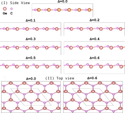
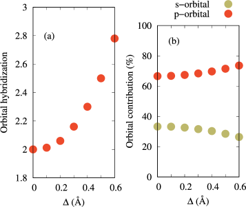
The degree of the hybridization of the - and the -orbitals can be found using a simple equation, , where is the angle between the equivalent orbitals, and [35]. The considered values of planar buckling affect the orbital hybridization. Most flat monolayers have an hybridization, and the orbital hybridization is approaching an configuration when the planar buckling is increased [36, 37]. A flat GeC monolayer () has an hybridization as is presented in Fig. 2(a), where the degree of the orbital hybridization is indicating an -hybridization at , and the degree of orbital hybridization is approaching when the planar buckling is increased to Å. The maximum allowed value of planar buckling for a GeC monolayer is Å in which the orbital hybridization is . The orbital hybridization is correlated with the buckling parameter in Tab. 1 for all values considered.
| Degree of hybridization | Ef (eV) | Ge-C (Å) | |
|---|---|---|---|
| 0.0 | sp2 | - | 1.858 |
| 0.1 | sp2.012 | 0.0665 | 1.861 |
| 0.2 | sp2.06 | 0.2677 | 1.869 |
| 0.3 | sp2.16 | 0.6111 | 1.882 |
| 0.4 | sp2.3 | 1.1126 | 1.901 |
| 0.5 | sp2.5 | 1.7992 | 1.924 |
| 0.6 | sp2.78 | 2.7089 | 1.952 |
Increasing planar buckling leads to a change in the ratio between the - and the -orbital contribution. For instance, the ratio of the - and the -orbitals are and , respectively, for a flat GeC monolayer, that displays an -hybridization as is seen in Fig. 2(b). Their ratio is changed to and for a buckled GeC with Å indicating the role of the -orbitals is decreases, while that of the the -orbital increases, when the planar buckling is increased. This can be understood by the bonding character of the monolayer in which strong bonds are formed through the orbital overlapping for a flat GeC, whereas the planar buckling reduces the overlapping and the bond symmetry is broken simultaneously as it approaches an overlapping. As a result, the -bonds become stronger through the -orbitals.
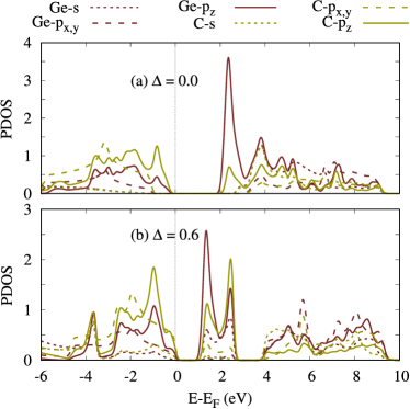
To confirm the modification of the - and the -bonds, we present the density of states of the - and the -orbitals (partial density of states, PDOS) for Ge and C atoms in Fig. 3 for a flat GeC, (a), and a buckled GeC with Å (b). The orbital contribution of the C atoms is dominant in the valence band region (below the Fermi energy, EF), while the Ge atoms have a higher orbital contribution in the conduction region. It can be seen that the density of states of the -orbitals is increased with planar buckling indicating that the bonds become stronger due to the planar buckling. On the other hand the density of states of the -orbitals for the Ge atoms in the conduction region is decreased with increasing .
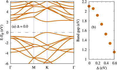
One can estimate the band gap of the GeC structure from the density of state in which the PDOS of both the and the orbitals of both atoms are shifted towards the Fermi energy resulting in a band gap reduction in the case of planar buckling. The band gap of a flat GeC is found to be eV, which is in a good agreement with the literature [38]. The band structure of a flat GeC monolayer is shown in Fig. 4(a) in addition to the band gap plotted as a function of the buckling parameter in (b). The calculated electronic band structure indicates that the flat GeC monolayer is a direct band gap semiconductor, with both the valence band maximum and conduction band minimum located at the K-point. The valence band maxima and the conduction band minima are composed of and bands which come from the C-2 and the Ge-4 orbitals extending above and below the GeC monolayer.
Increasing planar buckling reduces the band gap (see Fig. 4(b)) and the band gap is found to be eV at Å. Furthermore, a direct to indirect band gap transition occurs when the planar buckling is considered, especially at the high value of planar buckling when Å. The valence band maxima and the conduction band minima in the presence of the buckling come from the combined C-2, C-2 and the Ge-4 orbitals, respectively.
The formation energy, , is an important parameter to determine whether a structure is stable or not. The formation energy demonstrates the structural stability of the buckled GeC monolayers in comparison to a flat GeC monolayer. The values for a flat and the buckled GeC monolayers with different buckling strength are listed in Tab. 1. A GeC monolayer is stable for low values of , but our calculations show that the formation energy increases with increasing . As the planar buckling increases, a GeC monolayer becomes less energetically stable. The same situation was seen for other monolayers, where the stability of a monolayer decreases with increasing planar buckling [36]. Additionally, the Ge-C bond length is elongated with increasing (see Tab. 1). This leads to a symmetry breaking and thus affects the band structure and the band gap , that is reduced with increasing Ge-C bond length.
3.2 Thermal properties
In this section, we present the phonon band structure and heat capacity of the GeC monolayers and show how the planar buckling affects their thermal stability and heat capacity.
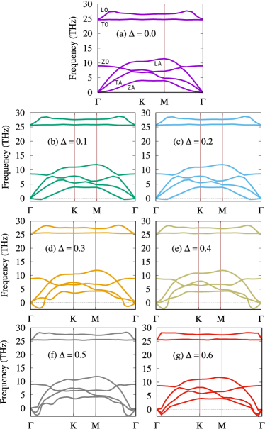
We first take a look at the phonon band structure along the high symmetry directions shown in Fig. 5. The phonon band structure of a flat GeC monolayer, , (Fig. 5 a) has no imaginary frequencies indicating the dynamical stability of the monolayer. The phonon band structure is plotted for a unit cell of a GeC containing two atoms. We thus see six phonon branches grouped into three acoustic and three optical ones. The acoustic phonon modes are in-plane longitudinal acoustic (LA), in-plane transverse acoustic (TA), and out-of-plane acoustic (ZA). In the same way, the optical phonon modes are in-plane longitudinal optical (LO), in-plane transverse optical (TO), and out-of-plane optical (ZO). One can clearly see that the width of acoustic bands is much smaller than the phonon band gap (13.16 THz), which is important for the phonon transport. The large band gap here can be related to the different atomic weights of Ge and C atom as the Ge atom is much heavier than a C atom. The transverse acoustic modes (in- and out-of-plane) are not degenerate due to the structural anisotropy. Additionally, while the LA and TA modes have a linear dispersion close to the -point, the (ZA) phonons exhibit a quadratic dispersion around -point. The parabolic dispersion of ZA modes is a characteristic feature of layered materials. All properties of the phonon band structure of a flat GeC monolayer are very well in agreement with the literature [39].
In the presence of planar buckling, , negative phonon frequencies are seen, especially for Å indicating dynamically unstable structures. At Å, only the ZA mode becomes negative in the vicinity of the -point and the negativity is further increased until all three acoustic modes become negative at the -point, when Å. In addition, the phonon band gap is slightly increased in the presence of planar buckling affecting the thermal properties of the system.
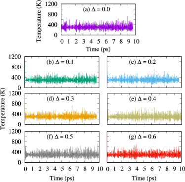
The thermal stability of a flat and buckled GeC is checked for approximately ps with a time step of fs as is presented in Fig. 6. The temperature curve of the pure and the buckled GeC monolayers neither displays large fluctuations in the temperature nor serious structure disruptions or bond breaking at K. This indicates that the pure and the buckled GeC monolayers are thermodynamically stable structures.
In Fig. 7, the heat capacity of a flat or buckled GeC monolayers is plotted. The heat capacity is the ratio of the heat absorbed by a material to the temperature change. The heat capacity indicates not only the thermal energy stored within a body but also how quickly the body cools or heats. As expected, the heat capacity of flat and buckled GeC monolayers increases with temperature, but the heat capacity is decreased with increasing planar buckling and the rate of the reduction is linear up to Å. This is caused by the lifting of the crossings of ZO mode with TA and LA modes in the case of and Å, which has a significant effect on phonon scattering processes. In the case of higher value of planar buckling, Å, there is no linear relation between the heat capacity and the buckling . We can not rely on the results for the heat capacity as the negativity in the phonon modes is high in this range of planar buckling.

3.3 Optical properties
The optical properties in the first-principles calculations are defined by the dielectric function. The complex dielectric function reflects the linear response of the semiconductor materials to an electromagnetic radiation. The random phase approximation (RPA) is utilized to calculate the complex dielectric function with a very dense mesh grid, , in the Brillouin zone to obtain accurate results [40]. In addition, we calculate the refractive index, the electron energy loss spectra (EELS), and the optical conductivity.
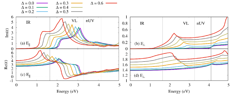
We first consider the imaginary and the real parts of the dielectric function shown in Fig. 8 for the parallel, E∥, (a) and perpendicular, E⟂, (b) polarization of the incoming electric field. We focus on different regions of the electromagnetic spectrum that are highlighted via the vertical lines including the infrared, IR, ( eV), the visible regime, VL, ( eV), and the near ultraviolet, nUV, ( eV). For crystalline materials, the Im() is an important parameter that is associate with photon absorption. An anisotropy of this optical parameter can clearly be seen when comparing the results for the two polarization directions for both flat and planar buckled GeC monolayers.
In the absence of planar buckling, the main intensity peak in Im() (purple) for a flat GeC monolayer appears at eV in the case of . The peak starts at eV reflecting a transition over the optical band gap. The main intensity peak is attributed to the electronic transition from C-pz in the valence band to Ge-pz in the conduction band (see Fig. 3(a)). The main intensity peak is found in the VL region. Additionally, a very small peak (not significant) in Im() for a flat GeC is found at eV in the selected range of the electromagnetic spectrum for . In the presence of planar buckling, the main intensity peak in E∥ is red shifted to a lower energy with higher intensity but it still remains in the VL region. This peak corresponds to the same transition from C-pz in the valence band to Ge-pz in the conduction band. Furthermore, a new peak is seen in the IR region at eV for the higher value of planer buckling, Å. The intensity of the new peak is increased with , and the new peak is red shifted with increasing . The new peak can be attributed to the electronic transition from C-px,y in the valence band to Ge-s or Ge-pz in the conduction band (see Fig. 3(b)). This is caused by the planar buckling effect redistributing the the orbital hybridization and the contribution of the density of states of the s- and p-orbitals. We notice that the same applies for the , but the new peak here appears in the VL region. The zero value of Im() in the IR region for both directions indicates the semiconductor behavior of both the flat and the planar buckled GeC.
The real part of the dielectric function is an important physical parameter that can determine the static dielectric constant (Re()) and the refractive index of the material. The real part of the dielectric function, Re(), is presented in Fig. 8(c) and (d) for E∥, and E⟂, respectively. The static dielectric constant is defined as the real part of the dielectric function at zero value of the incident photon energy or frequency. It can be seen that the static dielectric constant, Re(), of a flat GeC is for E∥ and for E⟂ for zero frequency. The static dielectric constants for both polarization directions of the electric field agree with previous DFT calculations [38]. The value of the static dielectric constant confirms that the flat GeC monolayer is a low dielectric material () and has semiconductor properties. By increasing the planar buckling, , the static dielectric function is increased to for E∥ and for E⟂ at Å, respectively. The finite values of Re() show the semiconducting character of the monolayers. This demonstrates that the planar buckling enhances the GeC monolayer from low to high dielectric material especially for E∥. Compared to a flat GeC, with the main peak of the real part at eV, it is red shifted for the buckled layers from the VL to the IR region for E∥.
Another remarkable point for the real part of the dielectric function is the plasmon energy or frequency. Plasmons can be determined by the real component of the dielectric function and are collective oscillations of the valence or the conduction electrons in a material. This is typically described by a material’s complex dielectric function, in which the real component describes the electromagnetic wave transmission through the medium and the imaginary component describes single particle excitations or the damping of the collective mode, due to interband transitions [41, 42]. There are two elements indicating the presence of plasmon oscillations. The real part of dielectric function changes sign or approaches a low value at the plasmon energy and there is a sharp drop in the Im() curve to be seen as the Re approaches zero [43, 44]. Therefore, the flat GeC monolayer shows indications for a plasmon mode at eV for E∥ as there is a sharp drop in Im() and the Re() approaches zero. The plasmon frequency for the buckled GeC monolayer is red shifted to the VL region at and Å for E∥ as the the real part of dielectric function drops and a minimum value in Im() is found. Additionally, no clear signs of plasmon oscillations is found for planar GeC for the E⟂ polarization.
Another optical characteristic is the refractive index, . In general, the behavior of follows qualitatively the characteristics of the real part of the dielectric function as presented in Fig. 9 for both polarization directions of the incoming electric field. Large values display strong interactions between the incident photons and the valence electrons, which cause a reduction in the photon speed during the transmission.
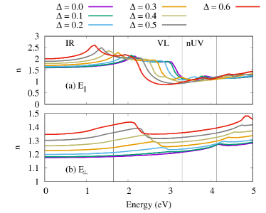
The refractive index of a flat GeC monolayer at zero energy or frequency limit, , is and , for E∥ (a), and E⟂ (b), respectively. In the presence of planar buckling, is increased to and at Å for E∥ (a), and E⟂ (b), respectively.
According to the refractive index curves in Fig. 9(a), the refractive index has its lowest value at eV (nUV region), which indicates weak interactions between the incident photons and the valence electrons. In this case, most of the light entering the flat GeC at this energy range passes through the monolayer, indicating a transparent material. The minimum value of the refractive index is red shifted to the VL region, when the planar buckling is increased to Å. It means that the transparency occurs at lower incident photon energy, when the planar buckling is considered. This is due to the weakness of the bond in the buckled GeC monolayer leading to more transparent material at lower photon energy. The maximum value of is seen in the IR region for E∥, and in the VL region for the E⟂. This demonstrates that a strong interaction between the incident photons and the valence electrons occurs in the IR and the VL regions for E∥ and E⟂, respectively.
Next, we discuss the electron energy loss spectra (EELS) presented in Fig. 10. The EELS introduces the loss of energy between the incident photons and GeC monolayer interaction. Again, the loss behavior for the two polarization directions is different. Each peak in the loss curve demonstrates a significant energy loss for the incident photons. In general, the reason for the EELS may be plasmonic oscillations or absorption or refraction of light in matter.
The first significant peak of EELS is seen at eV (nUV region) for a flat GeC in the E∥ direction. This peak is attributed to the plasmon oscillations shown in Fig. 8(a) and (c), whereas the effects of the refraction and the absorption do not play any role at this photon energy as is demonstrated in Fig. 9(a) and Fig. 11(a), respectively.
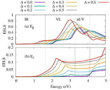
Considering the buckled GeC, the maximum peak is red shifted with a higher energy loss at higher values of the planar buckling for both polarization directions. In the E∥ direction, the maximum peak is found at eV in which the imaginary part of dielectric function has maximum value and the real part of dielectric function is zero. This loss peak is again due to damped plasmon oscillations.
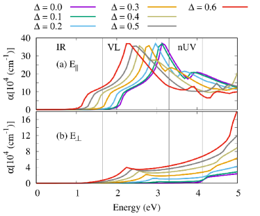
The absorption coefficient () for flat and buckled GeC monolayers for both the E∥ (a), and the E⟂ (b) is shown in Fig. 11. The zero value of indicates that the GeC monolayer is not a good conductor at low photon energy for both polarization directions. As the energy of the incident light increases, the absorption percentage increases in the VL region and the most intense peak is red shifted with increasing buckling, but remains in the VL region. The absorption characteristics in the photon energy of eV in the E∥ polarization direction can well be explained by the optical transition from the maximum of the valence band to the minimum of the conduction band in the band gap region.
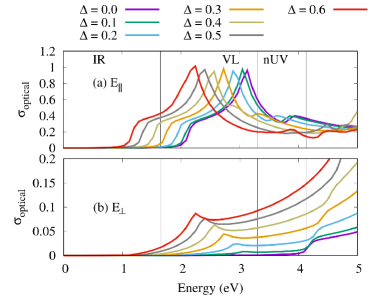
Finally, the optical conductivity (real part), , for flat and buckled GeC monolayers is displayed in Fig. 12. The optical conductivity follows the same qualitative property of the absorption spectra. Wherever there is a peak in the absorption spectra at a specific photon energy, a peak is found in the optical conductivity for almost the same photon energy. This confirms that the optical conductivity is generated by the absorption of photons by the electrons in a specific energy level transferring the electrons to higher energy levels. This process can include both intraband and interband transitions.
4 Conclusions
In summary, we have used density functional theory to study the properties of a Germagraphene, GeC, monolayer by considering the buckling effects. The GGA-PBE functionals with full potential augmented plane waves has been used in the calculations. The findings for the electronic properties indicate that planar buckling results in a tunable band gap, and the energy band gap decrease by increasing planar buckling. This is due to redistribution of orbital hybridization and the contribution ratio of the - and the -orbitals. The band gap change can tune the thermal properties and improve the optical behavior in the visible light, the VL, range. The results for the optical properties demonstrate that all features of the optical spectra get red-shifted to lower energy with increasing planar buckling. The band gap reduction significantly enhances the absorption spectra in the VL region. Consequently, the optical conductivity of buckled GeC is increased. Additionally, the heat capacity of flat and buckled GeC monolayers rises with temperature, but it falls with increasing planar buckling.
5 Acknowledgment
This work was financially supported by the University of Sulaimani and the Research center of Komar University of Science and Technology. The computations were performed on resources provided by the Division of Computational Nanoscience at the University of Sulaimani.
References
-
[1]
M. C. Lemme, D. Akinwande, C. Huyghebaert, C. Stampfer,
2D materials for future
heterogeneous electronics, Nature Communications 13 (1) (2022) 1392.
doi:10.1038/s41467-022-29001-4.
URL https://doi.org/10.1038/s41467-022-29001-4 -
[2]
K. F. Mak, C. Lee, J. Hone, J. Shan, T. F. Heinz,
Atomically
thin : A new direct-gap semiconductor, Phys. Rev. Lett.
105 (2010) 136805.
doi:10.1103/PhysRevLett.105.136805.
URL https://link.aps.org/doi/10.1103/PhysRevLett.105.136805 -
[3]
N. R. Abdullah, H. O. Rashid, V. Gudmundsson,
Study
of BC14N-bilayer graphene: Effects of atomic spacing and interatomic
interaction between B and N atoms, Superlattices and Microstructures 156
(2021) 106981.
doi:https://doi.org/10.1016/j.spmi.2021.106981.
URL https://www.sciencedirect.com/science/article/pii/S0749603621001798 -
[4]
L. Xiao, L. Youji, C. Feitai, X. Peng, L. Ming,
Facile synthesis of mesoporous
titanium dioxide doped by Ag-coated graphene with enhanced visible-light
photocatalytic performance for methylene blue degradation, RSC Adv. 7 (2017)
25314–25324.
doi:10.1039/C7RA02198D.
URL http://dx.doi.org/10.1039/C7RA02198D -
[5]
N. Tang, Y. Li, F. Chen, Z. Han, In
situ fabrication of a direct z-scheme photocatalyst by immobilizing CdS
quantum dots in the channels of graphene-hybridized and supported mesoporous
titanium nanocrystals for high photocatalytic performance under visible
light, RSC Adv. 8 (2018) 42233–42245.
doi:10.1039/C8RA08008A.
URL http://dx.doi.org/10.1039/C8RA08008A -
[6]
D. Akinwande, C. Huyghebaert, C.-H. Wang, M. I. Serna, S. Goossens, L.-J. Li,
H. S. P. Wong, F. H. L. Koppens,
Graphene and two-dimensional
materials for silicon technology, Nature 573 (7775) (2019) 507–518.
doi:10.1038/s41586-019-1573-9.
URL https://doi.org/10.1038/s41586-019-1573-9 -
[7]
A. Ramasubramaniam, A. R. Muniz,
Ab initio studies
of thermodynamic and electronic properties of phosphorene nanoribbons, Phys.
Rev. B 90 (2014) 085424.
doi:10.1103/PhysRevB.90.085424.
URL https://link.aps.org/doi/10.1103/PhysRevB.90.085424 -
[8]
D. V. Shtansky, K. L. Firestein, D. V. Golberg,
Fabrication and application of BN
nanoparticles, nanosheets and their nanohybrids, Nanoscale 10 (2018)
17477–17493.
doi:10.1039/C8NR05027A.
URL http://dx.doi.org/10.1039/C8NR05027A -
[9]
V. P. Kumar, D. K. Panda,
Review-next generation 2D
material molybdenum disulfide (MoS2: Properties, applications and
challenges, ECS Journal of Solid State Science and Technology 11 (3)
(2022) 033012.
doi:10.1149/2162-8777/ac5a6f.
URL https://doi.org/10.1149/2162-8777/ac5a6f -
[10]
N. R. Abdullah, B. J. Abdullah, H. O. Rshid, C.-S. Tang, A. Manolescu,
V. Gudmundsson,
Enhanced
electronic and optical responses of nitrogen- or boron-doped BeO monolayer:
First principle computation, Superlattices and Microstructures 162 (2022)
107102.
doi:https://doi.org/10.1016/j.spmi.2021.107102.
URL https://www.sciencedirect.com/science/article/pii/S0749603621003037 -
[11]
N. R. Abdullah, B. J. Abdullah, V. Gudmundsson,
High
thermoelectric and optical conductivity driven by the interaction of boron
and nitrogen dopant atoms with a 2D monolayer beryllium oxide, Materials
Science in Semiconductor Processing 141 (2022) 106409.
doi:https://doi.org/10.1016/j.mssp.2021.106409.
URL https://www.sciencedirect.com/science/article/pii/S136980012100740X -
[12]
Y. Ji, H. Dong, T. Hou, Y. Li,
Monolayer graphitic germanium
carbide (g-GeC): the promising cathode catalyst for fuel cell and
lithium–oxygen battery applications, J. Mater. Chem. A 6 (2018)
2212–2218.
doi:10.1039/C7TA10118J.
URL http://dx.doi.org/10.1039/C7TA10118J -
[13]
T. Suzuki, Y. Yokomizo,
Energy
bands of atomic monolayers of various materials: Possibility of energy gap
engineering, Physica E: Low-dimensional Systems and Nanostructures 42 (10)
(2010) 2820–2825, 14th International Conference on Modulated Semiconductor
Structures.
doi:https://doi.org/10.1016/j.physe.2010.04.031.
URL https://www.sciencedirect.com/science/article/pii/S1386947710002729 -
[14]
I. Guilhon, L. K. Teles, M. Marques, R. R. Pela, F. Bechstedt,
Influence of
structure and thermodynamic stability on electronic properties of
two-dimensional SiC, SiGe, and GeC alloys, Phys. Rev. B 92 (2015) 075435.
doi:10.1103/PhysRevB.92.075435.
URL https://link.aps.org/doi/10.1103/PhysRevB.92.075435 - [15] S. Kumar, H. Trodahl, Thin films of amorphous germanium-carbon and germanium-nitrogen alloys prepared by activated reactive evaporation, Thin solid films 193 (1990) 72–76.
- [16] H. Jamali, R. Mozafarinia, A. Eshaghi, Effect of deposition parameters on the microstructure and deposition rate of Germanium-Carbon coatings prepared by plasma enhanced chemical vapor deposition, Surface and Coatings Technology 302 (2016) 107–116.
- [17] N. Gupta, B. P. Veettil, H. Xia, S. K. Karuturi, G. Conibeer, S. Shrestha, Synthesis of nano-crystalline Germanium Carbide using radio frequency magnetron sputtering, Thin Solid Films 592 (2015) 162–166.
-
[18]
A. G. Gökçe, F. Ersan,
Adsorption of alkali and
alkaline earth metal atoms and dimers on monolayer germanium carbide,
Philosophical Magazine 97 (3) (2017) 155–167.
arXiv:https://doi.org/10.1080/14786435.2016.1248517, doi:10.1080/14786435.2016.1248517.
URL https://doi.org/10.1080/14786435.2016.1248517 -
[19]
T. V. Vu, N. T. T. Anh, D. Hoat, D. P. Tran, H. D. Tong, H. L. Luong, L. M.
Hieu, C. V. Nguyen, H. V. Phuc, N. T. Binh, N. N. Hieu,
Electronic,
optical and photocatalytic properties of fully hydrogenated GeC monolayer,
Physica E: Low-dimensional Systems and Nanostructures 117 (2020) 113857.
doi:https://doi.org/10.1016/j.physe.2019.113857.
URL https://www.sciencedirect.com/science/article/pii/S1386947719316200 -
[20]
Z. Sohbatzadeh, H. A. Eivari, D. V. Fakhrabad,
Formation
energy and some mechanical properties of hydrogenated hexagonal monolayer of
GeC, Physica B: Condensed Matter 547 (2018) 88–91.
doi:https://doi.org/10.1016/j.physb.2018.08.009.
URL https://www.sciencedirect.com/science/article/pii/S0921452618304939 -
[21]
L. Drissi, F. Ramadan, N.-J. Kanga,
Fluorination-control
of electronic and magnetic properties in GeC-hybrid, Chemical Physics
Letters 659 (2016) 148–153.
doi:https://doi.org/10.1016/j.cplett.2016.07.017.
URL https://www.sciencedirect.com/science/article/pii/S0009261416304973 -
[22]
T. V. Vu, N. T. T. Anh, D. P. Tran, D. Hoat, N. T. Binh, H. D. Tong, B. D. Hoi,
C. V. Nguyen, H. V. Phuc, N. N. Hieu,
Surface
functionalization of GeC monolayer with F and Cl: Electronic and optical
properties, Superlattices and Microstructures 137 (2020) 106359.
doi:https://doi.org/10.1016/j.spmi.2019.106359.
URL https://www.sciencedirect.com/science/article/pii/S0749603619319044 -
[23]
P. Giannozzi, S. Baroni, N. Bonini, M. Calandra, R. Car, C. Cavazzoni,
D. Ceresoli, G. L. Chiarotti, M. Cococcioni, I. Dabo, A. D. Corso,
S. de Gironcoli, S. Fabris, G. Fratesi, R. Gebauer, U. Gerstmann,
C. Gougoussis, A. Kokalj, M. Lazzeri, L. Martin-Samos, N. Marzari, F. Mauri,
R. Mazzarello, S. Paolini, A. Pasquarello, L. Paulatto, C. Sbraccia,
S. Scandolo, G. Sclauzero, A. P. Seitsonen, A. Smogunov, P. Umari, R. M.
Wentzcovitch,
QUANTUM
ESPRESSO: a modular and open-source software project for quantum
simulations of materials, Journal of Physics: Condensed Matter 21 (39)
(2009) 395502.
doi:10.1088/0953-8984/21/39/395502.
URL https://doi.org/10.1088%2F0953-8984%2F21%2F39%2F395502 - [24] P. Giannozzi, O. Andreussi, T. Brumme, O. Bunau, M. B. Nardelli, M. Calandra, R. Car, C. Cavazzoni, D. Ceresoli, M. Cococcioni, et al., Advanced capabilities for materials modelling with quantum espresso, Journal of Physics: Condensed Matter 29 (46) (2017) 465901.
-
[25]
N. R. Abdullah, B. J. Abdullah, V. Gudmundsson,
Electronic
and optical properties of metallic nitride: A comparative study between the
MN (M = Al, Ga, In, Tl) monolayers, Solid State Communications 346 (2022)
114705.
doi:https://doi.org/10.1016/j.ssc.2022.114705.
URL https://www.sciencedirect.com/science/article/pii/S0038109822000527 -
[26]
N. R. Abdullah, H. O. Rashid, C.-S. Tang, A. Manolescu, V. Gudmundsson,
Controlling
physical properties of bilayer graphene by stacking orientation caused by
interaction between B and N dopant atoms, Materials Science and Engineering:
B 276 (2022) 115554.
doi:https://doi.org/10.1016/j.mseb.2021.115554.
URL https://www.sciencedirect.com/science/article/pii/S0921510721005080 -
[27]
N. R. Abdullah, B. J. Abdullah, H. O. Rashid, C.-S. Tang, V. Gudmundsson,
Modulation
of electronic and thermal proprieties of TaMoS2 by controlling the repulsive
interaction between Ta dopant atoms, Solid State Communications 342 (2022)
114590.
doi:https://doi.org/10.1016/j.ssc.2021.114590.
URL https://www.sciencedirect.com/science/article/pii/S0038109821003732 -
[28]
G. J. Martyna, M. L. Klein, M. Tuckerman,
Nosé–Hoover chains: The canonical
ensemble via continuous dynamics, The Journal of Chemical Physics 97 (4)
(1992) 2635–2643.
,doi:10.1063/1.463940.
URL https://doi.org/10.1063/1.463940 -
[29]
Q. Zhang, F. Zhang,
New
honeycomb-like M-based (M = C, Si, Ge and Sn) monochalcogenides polymorphs:
An extended family as isoelectronic photocatalysts of group-va for water
splitting, Applied Surface Science 554 (2021) 149644.
doi:https://doi.org/10.1016/j.apsusc.2021.149644.
URL https://www.sciencedirect.com/science/article/pii/S0169433221007200 -
[30]
M. Goudarzi, S. Parhizgar, J. Beheshtian,
Electronic
and optical properties of vacancy and B, N, O and F doped graphene: DFT
study, Opto-Electronics Review 27 (2) (2019) 130–136.
doi:https://doi.org/10.1016/j.opelre.2019.05.002.
URL https://www.sciencedirect.com/science/article/pii/S1230340218301021 - [31] M. Dressel, G. Grüner, Electrodynamics of solids: optical properties of electrons in matter (2002).
-
[32]
Q. Zhang, X. Wang, S. Yang,
-sns: An emerging
bidirectional auxetic direct semiconductor with desirable carrier mobility
and high-performance catalytic behavior toward the water-splitting reaction,
ACS Applied Materials & Interfaces 13 (27) (2021) 31934–31946, pMID:
34196545.
arXiv:https://doi.org/10.1021/acsami.1c03650, doi:10.1021/acsami.1c03650.
URL https://doi.org/10.1021/acsami.1c03650 -
[33]
J. Mistrik, S. Kasap, H. E. Ruda, C. Koughia, J. Singh,
Optical Properties of
Electronic Materials: Fundamentals and Characterization, Springer
International Publishing, Cham, 2017, pp. 1–1.
doi:10.1007/978-3-319-48933-9_3.
URL https://doi.org/10.1007/978-3-319-48933-9_3 -
[34]
J. Wu, Y. Yang, H. Gao, Y. Qi, J. Zhang, Z. Qiao, W. Ren,
Electric field effect of GaAs
monolayer from first principles, AIP Advances 7 (3) (2017) 035218.
arXiv:https://doi.org/10.1063/1.4979507, doi:10.1063/1.4979507.
URL https://doi.org/10.1063/1.4979507 - [35] G. B. Kaufman, Inorganic chemistry: principles of structure and reactivity, (huheey, james e.; keiter, ellen a.; keiter, richard l.) (1993).
- [36] J. Jalilian, M. Safari, S. Naderizadeh, Buckling effects on electronic and optical properties of BeO monolayer: First principles study, Computational Materials Science 117 (2016) 120–126.
-
[37]
N. R. Abdullah, B. J. Abdullah, H. O. Rashid, C.-S. Tang, V. Gudmundsson,
Study
of the buckling effects on the electrical and optical properties of the group
III-nitride monolayers, Materials Science in Semiconductor Processing 150
(2022) 106943.
doi:https://doi.org/10.1016/j.mssp.2022.106943.
URL https://www.sciencedirect.com/science/article/pii/S1369800122004772 -
[38]
S. Behzad,
Direct
to indirect band gap transition in two-dimensional germanium carbide through
Si substitution, Results in Physics 13 (2019) 102306.
doi:https://doi.org/10.1016/j.rinp.2019.102306.
URL https://www.sciencedirect.com/science/article/pii/S2211379719302955 -
[39]
S.-D. Guo, X.-S. Guo, J. Dong,
Born effective charge removed
anomalous temperature dependence of lattice thermal conductivity in monolayer
GeC, Journal of Physics: Condensed Matter 31 (12) (2019) 125701.
doi:10.1088/1361-648x/aafd58.
URL https://doi.org/10.1088/1361-648x/aafd58 -
[40]
N. R. Abdullah, B. J. Abdullah, V. Gudmundsson,
DFT
study of tunable electronic, magnetic, thermal, and optical properties of a
Ga2Si6 monolayer, Solid State Sciences 125 (2022) 106835.
doi:https://doi.org/10.1016/j.solidstatesciences.2022.106835.
URL https://www.sciencedirect.com/science/article/pii/S1293255822000309 - [41] H. Raether, Excitation of plasmons and interband transitions by electrons, Vol. 88, Springer, 2006.
- [42] R. Egerton, An introduction to eels, in: Electron Energy-Loss Spectroscopy in the Electron Microscope, Springer, 2011, pp. 1–28.
-
[43]
S. Guan, S. A. Yang, L. Zhu, J. Hu, Y. Yao,
Electronic, dielectric and plasmonic
properties of two-dimensional electride materials X2N (X=Ca, Sr): A
first-principles study, Scientific Reports 5 (1) (2015) 12285.
doi:10.1038/srep12285.
URL https://doi.org/10.1038/srep12285 -
[44]
S. Esfandiari, R. Moradian,
Optical properties of
graphene-like Be3C2 monolayer by first-principles calculations, Journal of
the Physical Society of Japan 91 (7) (2022) 074707.
arXiv:https://doi.org/10.7566/JPSJ.91.074707, doi:10.7566/JPSJ.91.074707.
URL https://doi.org/10.7566/JPSJ.91.074707