∗ emarrufo@uchicago.edu
Design of a Skipper CCD Focal Plane for the SOAR Integral Field Spectrograph
Abstract
We present the development of a Skipper Charge-Coupled Device (CCD) focal plane prototype for the SOAR Telescope Integral Field Spectrograph (SIFS). This mosaic focal plane consists of four 6k 1k, 15 m pixel Skipper CCDs mounted inside a vacuum dewar. We describe the process of packaging the CCDs so that they can be easily tested, transported, and installed in a mosaic focal plane. We characterize the performance of m thick, fully-depleted engineering-grade Skipper CCDs in preparation for performing similar characterization tests on science-grade Skipper CCDs which will be thinned to 250m and backside processed with an antireflective coating. We achieve a single-sample readout noise of for the best performing amplifiers and sub-electron resolution (photon counting capabilities) with readout noise from 800 measurements of the charge in each pixel. We describe the design and construction of the Skipper CCD focal plane and provide details about the synchronized readout electronics system that will be implemented to simultaneously read 16 amplifiers from the four Skipper CCDs (4-amplifiers per detector). Finally, we outline future plans for laboratory testing, installation, commissioning, and science verification of our Skipper CCD focal plane.
keywords:
Skipper CCD, sub-electron noise, photon counting detector, spectroscopy1 INTRODUCTION
The Southern Astrophysical Research (SOAR) Telescope Integral Field Spectrograph (SIFS) is an astronomical spectrograph equipped with an optical fiber-lenslet integral field unit (IFU) [1]. SIFS was developed and constructed in Brazil by Laboratório Nacional de Astrofísica, Ministry of Science, Technology and Innovation (LNA/MCTI) in partnership with Instituto de Astronomia, Geofísica e Ciências Atmosféricas, Universidade de São Paulo (IAG/USP) for the 4.1-m SOAR telescope, located on Cerro Pachón in the Coquimbo Region of Chile. Integral field spectroscopy provides a spectrum for each spatial element in a two dimensional field; in the case of SIFS, data products consists of three-dimensional data cubes with axes of right accession, declination, and wavelength. The main science driver that has guided the design of SIFS is the study of complex extended objects such as H ii clouds and star-forming regions in galaxies by providing simultaneous spectra of such extended objects. The high spatial resolution of SIFS is of particular importance for the study of velocity fields and ionization structure in H ii regions, active galactic nuclei (AGN) [2], and planetary nebulae [3, 1].
Astronomical spectrographs disperse light over a large detector area. For faint astronomical sources, this results in low signal-to-noise in each detector pixel. This is a particularly common case in observations with SIFS, where signal-to-noise often is a limiting factor in scientific measurements (e.g., when constructing a velocity map far from the nucleus of an AGN) [1, 2]. In the low-signal-to-noise regime, detector readout noise can be an important contribution to the overall noise in an observation, affecting the sensitivity of spectroscopic measurements. Skipper CCDs offer a novel solution to the problem of detector readout noise by using a floating gate output stage to perform repeated measurements of the charge in each pixel. These measurements can be combined to reduce readout noise relative to a single measurement and achieve sub-electron resolution, i.e., single electron/photon counting. The Skipper CCD concept as a photosensitive detector was proposed in 1990 [4, 5]; however, in early demonstrations of this technology, the readout noise deviated from the theoretical expectation at , which prevented single photon counting [4]. In contrast, modern Skipper CCDs have achieved an order of magnitude lower readout noise and stable performance over a large area detector [6].
Here we present the development of a Skipper CCD focal plane prototype for SIFS [3]. Our goal is to demonstrate the low-readout noise capabilities of modern Skipper CCDs (targeting a reduction in the readout noise of SIFS), while exposing Skipper CCDs to the full complexities of astronomical spectroscopy for the first time. The Skipper CCD focal plane will replace the current SIFS dewar and detector with a dewar housing a mosaic focal plane of four 6k 1k Skipper CCDs. We will also replace the readout electronics with low-threshold readout boards designed for Skipper CCDs (Section 6). The reduction in readout noise that Skipper CCDs offer will improve SIFS’ signal-to-noise when imaging faint sources in the low-signal, low sky-background regime such as N ii or S ii spectral lines. In this paper, we describe the process for designing and testing the Skipper CCD focal plane for SIFS.
2 THE SKIPPER CCD for Astronomy
Skipper CCDs use a floating gate output stage to allow for multiple, non-destructive measurements of the charge in each pixel. Tiffenberg et al. (2017) [6] demonstrated that Skipper CCDs designed at Lawrence Berkeley National Laboratory (LBNL), fabricated at Teledyne DALSA, and packaged at Fermi National Accelerator Laboratory (Fermilab) could implement a floating-gate output stage, a small capacitance sense node, and isolation from parasitic noise sources to perform repeated, nondestructive measurements of the charge in each pixel of a thick, fully depleted Skipper CCD, achieving a readout noise of [6]. Subsequent testing has demonstrated that this new generation of Skipper CCDs can achieve readout noise values of [7]. The readout noise achieved after independent measurements, , follows the expected behavior from Gaussian statistics:
| (1) |
where is the single-sample readout noise (the standard deviation of pixel values with a single charge measurement per pixel) and is the number of measurements performed for each pixel [7].
| Characteristic | Value | Unit | Reference |
|---|---|---|---|
| Single-Sample Readout Noise | 2.5 | [8] | |
| Multi-Sample Readout Noise | 0.039 | [8] | |
| Dark Current | [9] | ||
| Spurious Clock-Induced Charge | /pix/frame | [9] | |
| Quantum Efficiency () | … | [10] | |
| Charge Transfer Inefficiency | … | [10] | |
| Full-Well Capacity | [10] |
In addition to having the capability to dynamically tune the readout noise on a pixel-by-pixel basis, Skipper CCDs maintained the well-characterized performance of the thick, fully depleted, -channel CCDs developed by LBNL for astronomy (i.e., stability, linear response, large dynamic range, high QE in the red and near infra-red regimes, and radiation tolerance) [10, 11]. Skipper CCDs have been extensively characterized in the literature (see Table 1), demonstrating unprecedented performance for particle physics and astronomical applications. In particular, we note the first optical characterizations of the Skipper CCD for cosmological applications [10], which informed the plans to test the Skipper CCD in a realistic astronomical observing scenario. In [10], we demonstrated that a backside illuminated Skipper CCD could achieve relative QE from 450 to 900, with relative QE out to 1. When compared to the absolute QE of LBNL CCDs developed for the Dark Energy Camera (DECam) and the Dark Energy Spectroscopic Instrument (DESI), we expect that it is possible to achieve QE from 450 to 950. Furthermore, we showed that the Skipper CCD achieved a full-well capacity of with a shallow voltage configuration, and we expect that by optimizing clock voltages, the Skipper CCD can achieve values , based on the performance of other thick, high resistivity CCDs from LBNL [12].
3 SOAR Integral Field Spectrograph
3.1 System Characteristics
The SOAR Telescope is a 4.1-m Ritchey-Chretien alt-azimuth telescope that provides high-precision pointing with a large instrument payload capacity and excellent angular resolution with tip-tilt correction [1, 13]. SIFS is a fiber-fed integral field spectrograph consisting of 1300 fibers covering a 15 7.8 arsec2 field-of view with an angular resolution of 0.30 arsec/fiber. This allows SIFS to perform spatially resolved 2D spectroscopy of complex extended objects and crowded fields. SIFS has wide wavelength coverage, from 350 nm to 1000 nm, while allowing for simultaneous spectra to be taken of all parts of moderately extended objects such as H ii regions. Furthermore, SIFS uses volume phase holographic (VPH) transmission gratings that offer a range of spectral resolution () from , which is sufficient to measure stellar metallicities at and abundance ratios, such as H/Fe, at [3, 1, 13]. For example, Palumbo et al. (2020) used SIFS to measure redshifts, velocity fields, which were constructed by sampling object spectra at many discrete points, specific start formation rates, and surface mass densities of compact dwarf starburst galaxies in the Local Volume [14]. Patrícia da Silva at al. (2020) presented a multi-wavelength study of the nuclear region of NGC 613, which contains an AGN. In this study, SIFS is used to obtain a data cube of the central region of NGC 613 with a spatial resolution of 0.3 arsec 0.3 arsec; the data is used to study H ii star-forming regions in the circumnuclear ring of the galaxy [2].
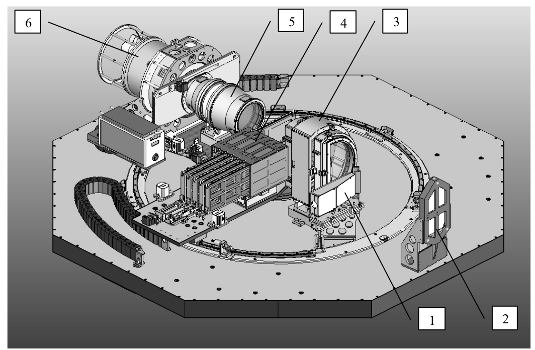
SIFS is composed of three main subsystems: the fore-optics, the IFU, and the bench spectrograph. The fore-optics consist of a magnification lens group followed by a field lens, which magnifies the focal plane of the telescope to the scale that is required by the micro lens array [1]. SIFS employs a lenslet, fiber IFU system which consists of 1300 lenslets and optical fibers arranged into a array and encapsulated in 26 furcation tubes. The optical fibers (Polymicro “blue” fiber) have a spectral transmission for wavelengths between 350 nm and 950 nm [1, 13]. The bench spectrograph (Fig. 1) is installed on the platform of the SOAR telescope, supported by six sets of pneumatic supports for vibration isolation. The bench spectrograph includes the output unit support, the collimator lens group and a spherical mirror, the VPH gratings exchanging mechanism, the camera and detector [13]. The SIFS Skipper CCD focal plane will house four Skipper CCDs and be mounted in a replacement cryostat that matches the mechanical dimensions and focal distance of the original (item 6 in Fig. 1). The modular design of the cryostat simplifies the time, cost and risk of installation since no mechanical or optical modifications are required; furthermore, there is not need to replace any other components of the bench spectrograph.
3.2 Expected Improvements from a Skipper CCD Focal Plane
| Characteristic | Value | Unit |
|---|---|---|
| Signal Rate | 0.01191 | |
| Background Rate | 0.0079 | |
| Dark Current | ||
| Readout Noise | 5.2 | |
| Npix | pix | |
| Readout Time | 22 | secs |
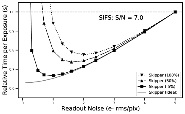
The SIFS bench spectrograph currently uses a thinned CCD231-84 from Teledyne e2v that has a format of 4096 4112 pixels and a pixel size of m. The detector is read through two channels in 22s with a readout noise of and a gain of /ADU. Table 2 shows some characteristic parameters that influence the SIFS performance, including the SIFS detector performance. We note that an evident improvement from the Skipper CCD focal plane will be the single sample per pixel readout noise. Assuming the Skipper CCD can reach a single sample readout noise of 3.5 , based on the performance of similar Skipper CCDs [10, 6, 15], there will be a improvement in readout noise when comparing with SIFS’s current detector.
In Fig. 2, we explore the observation time required to reach a fixed signal-to-noise (S/N) ratio as a function of readout noise for SIFS. First, we consider the S/N ratio for an astronomical observation, which can be interpreted as the sensitivity to a given source and is defined as the ratio between the number of counts contributed by the source and the total noise in the observation. Mathematically, S/N is expressed as
| (2) |
where represents the total noise in the observation, which includes the total electron rates () from the source, background, and dark contributions integrated over pixel elements (), added in quadrature, assuming uncorrelated pixel measurements, i.e. . Here, represents the readout noise of a Skipper CCD, which is an intrinsic property of the detector, independent of the integration time, and tunable or scalable by the number of samples per pixel, . The readout noise is quantified in units of the root-mean-square (rms) fluctuations in the number of electrons per pixel. Fig. 2, constructed with the values from Table 2, shows the expected improvement in the reduction of observation time (exposure + readout time) to reach a target signal-to-noise for different percentages of the detector being read out, i.e., region of interest functionality (Section 7).
4 SKIPPER CCD DETECTORS
4.1 Detector architecture and characteristics
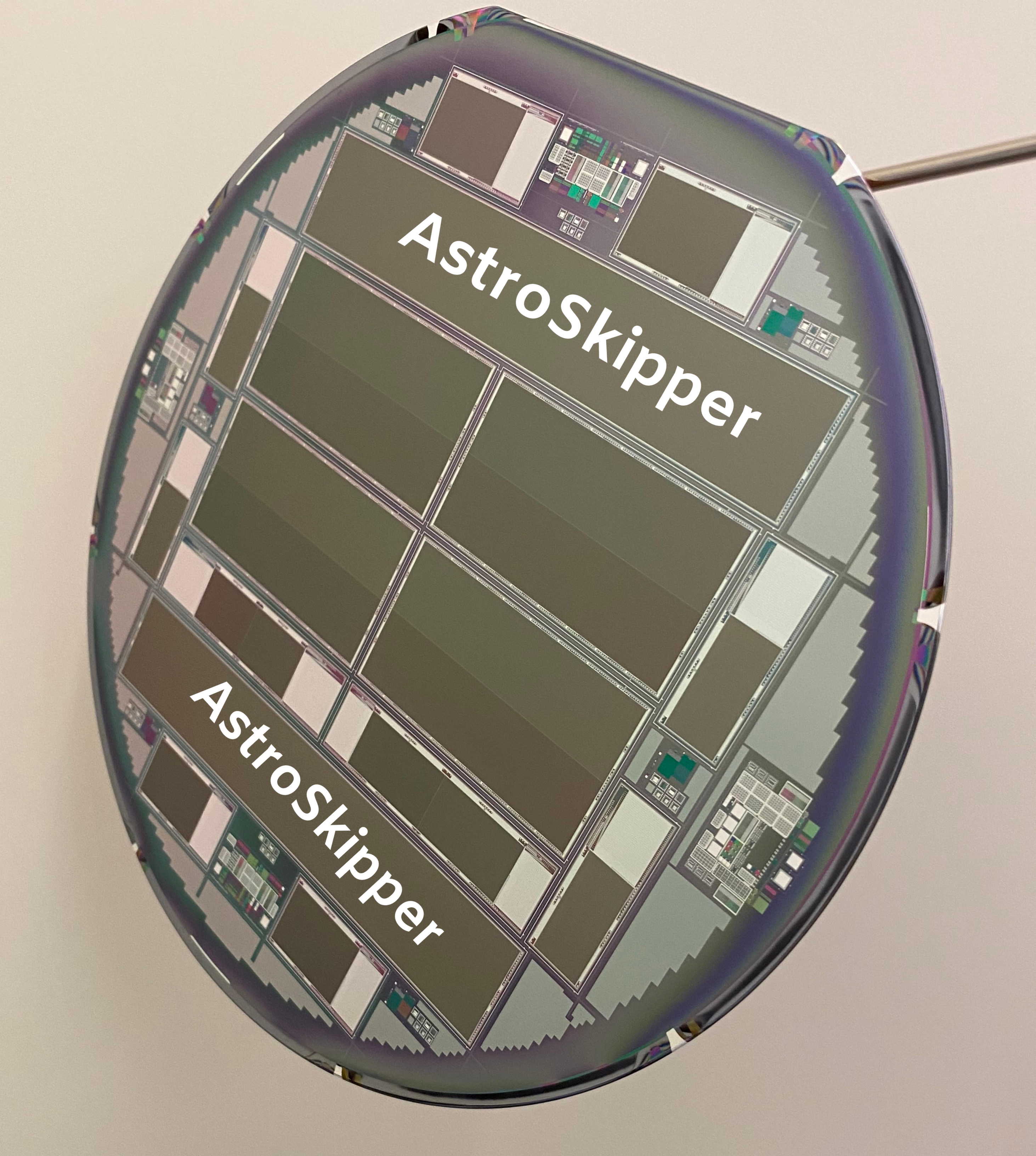
The four backside illuminated Skipper CCDs that will be used for the SIFS Skipper CCD focal plane come from a fabrication run for Fermilab R&D projects. The Skipper CCDs are -channel detectors fabricated on high resistivity (5 k), -type silicon. The wafers are fabricated at a thickness of , and will be thinned, and backside processed with an antireflective coating at the LBNL Microsystems Laboratory. Each silicon wafer contains 16 Skipper CCDs (Fig. 3) with different readout and size configurations. For the SIFS Skipper CCD focal plane, we will use standard wide-format Skipper CCDs (6k 1k, 15 m pixels) with four amplifiers (“AstroSkipper” in Fig. 3). The pixel scale of these detectors matches that of the existing SIFS e2v detector, and a mosaic of four 6k 1k Skipper CCD detectors will be used to cover the full 4k 4k pixel area of the current SIFS detector.
4.2 Detector Packaging
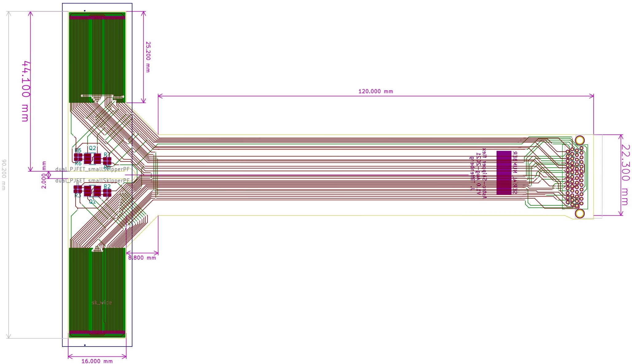
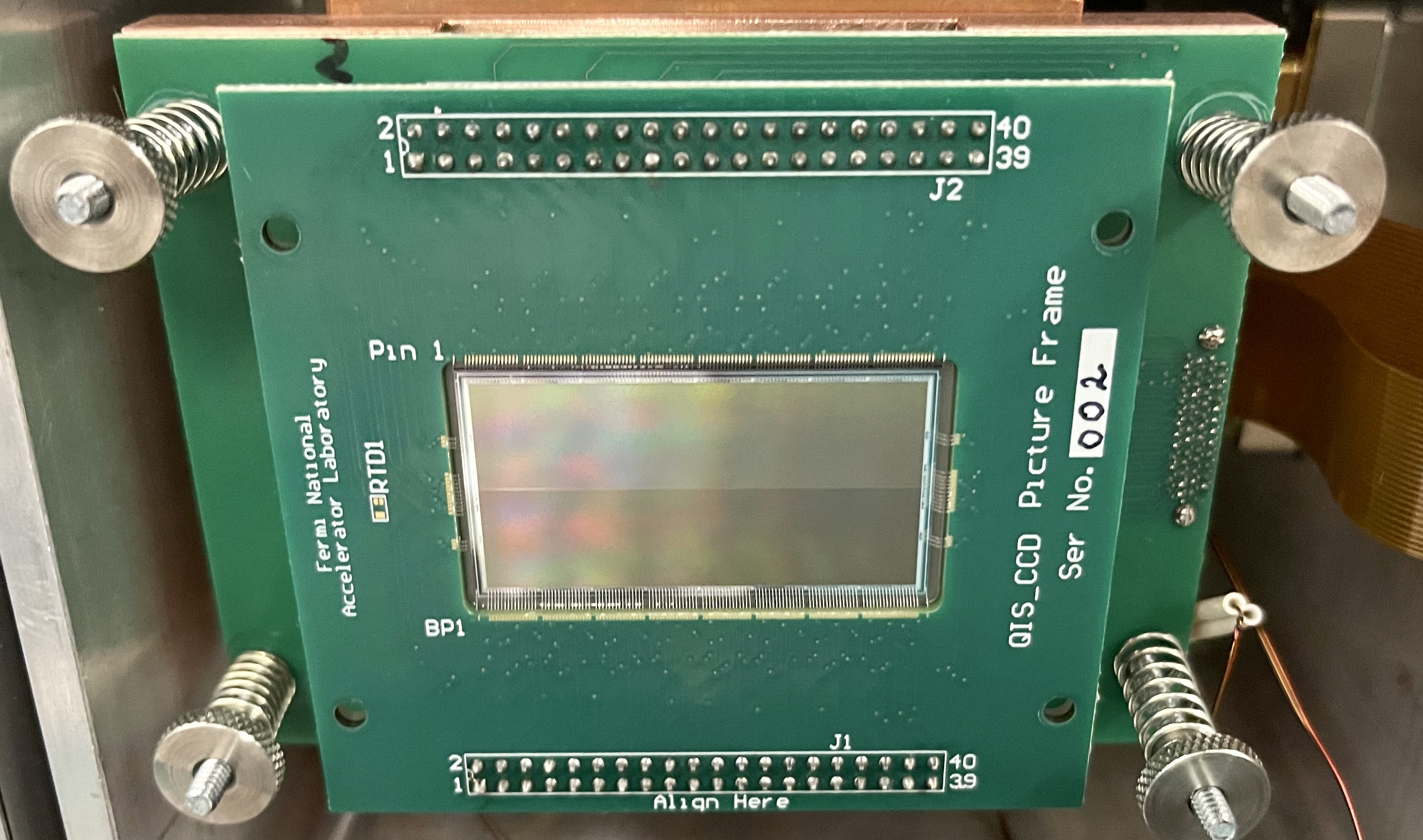
The AstroSkipper CCD detector package has two main components: a flexible cable for carrying electrical signals to/from the CCD and a mechanical foot for mounting the CCD to the focal plane. The flexible cable carries the bias voltages, clock voltages, and video signals and it has two junction-gate field-effect transistors (JFETs), four 20 k resistors, and a 51-pin Omnetics connector. We use two high performance dual LSJ689-SOT-23, -channel JFETs that provide ultra-low noise (nV/ ).
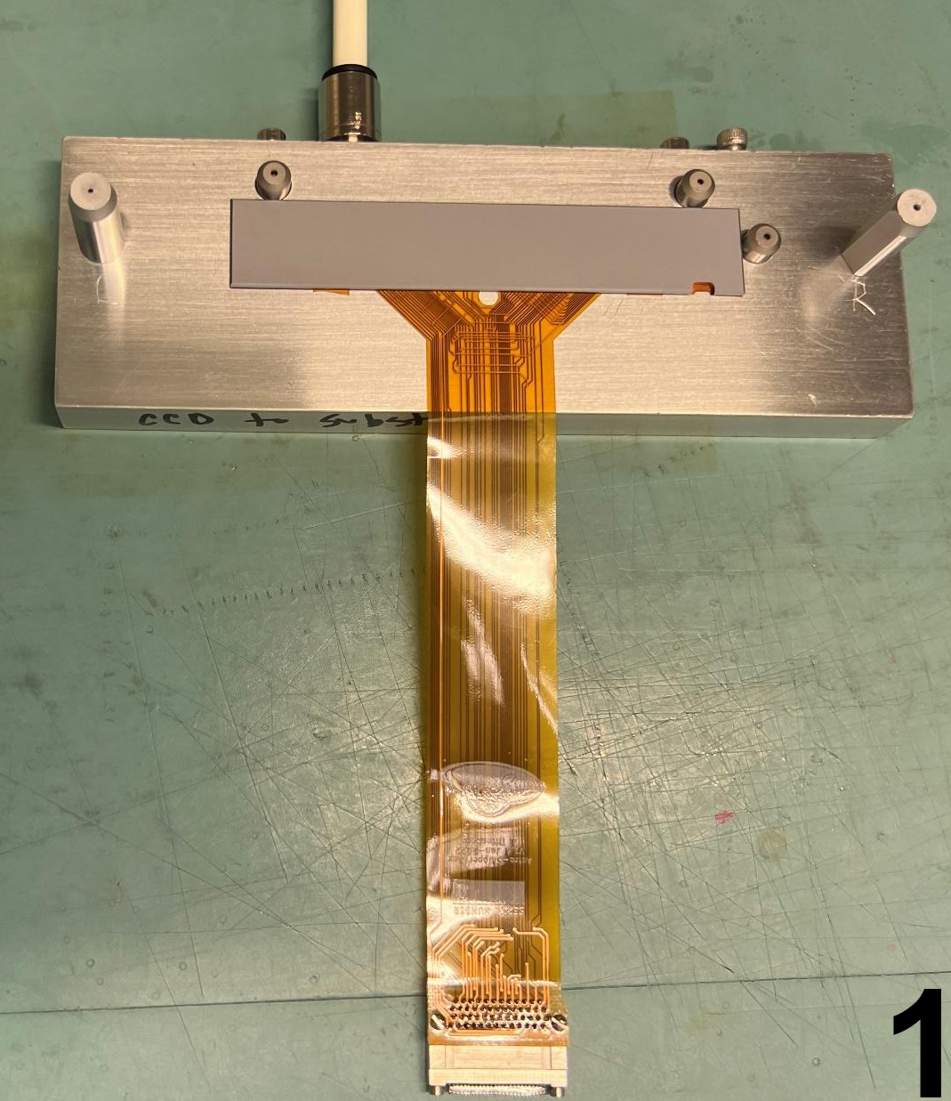
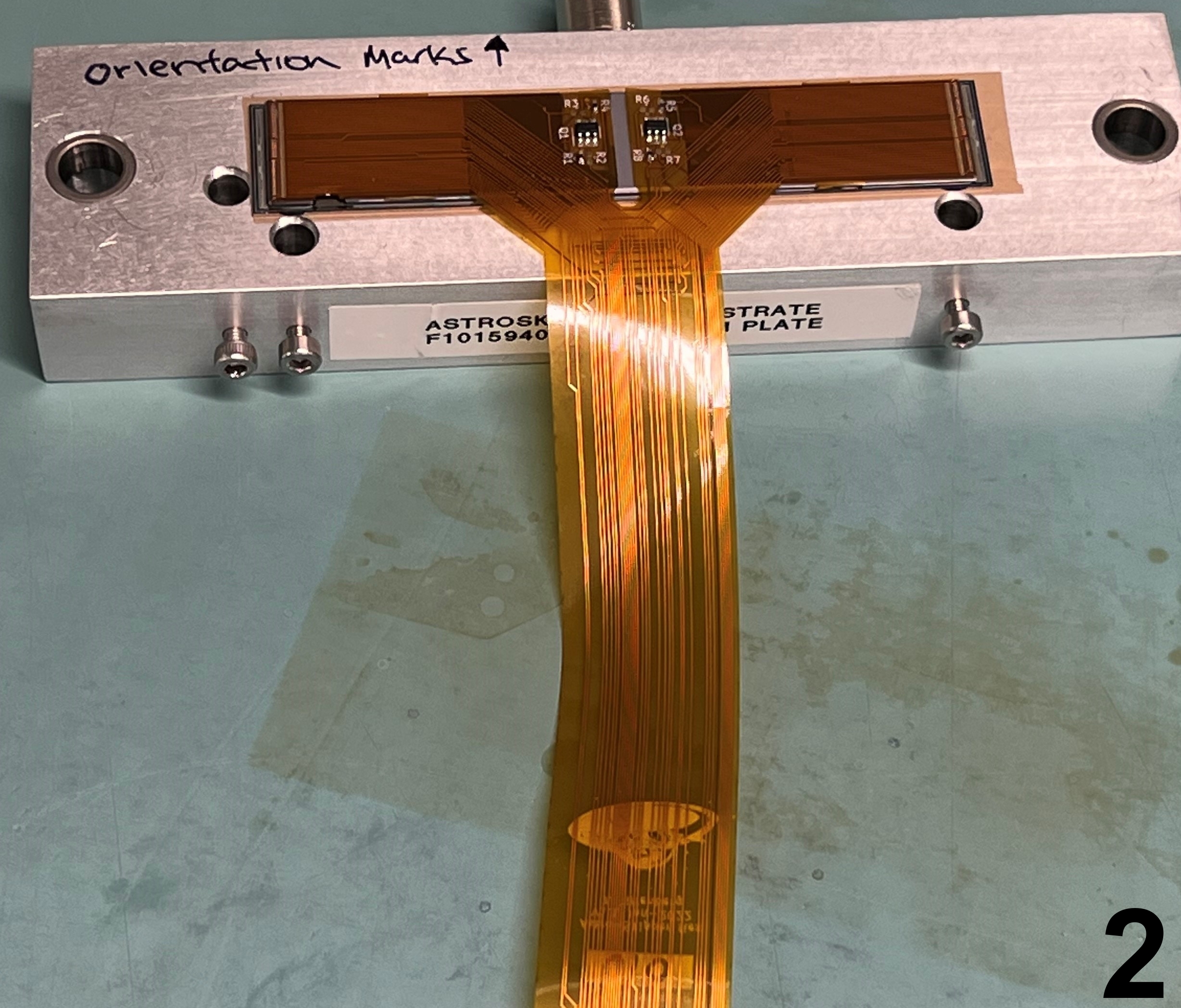
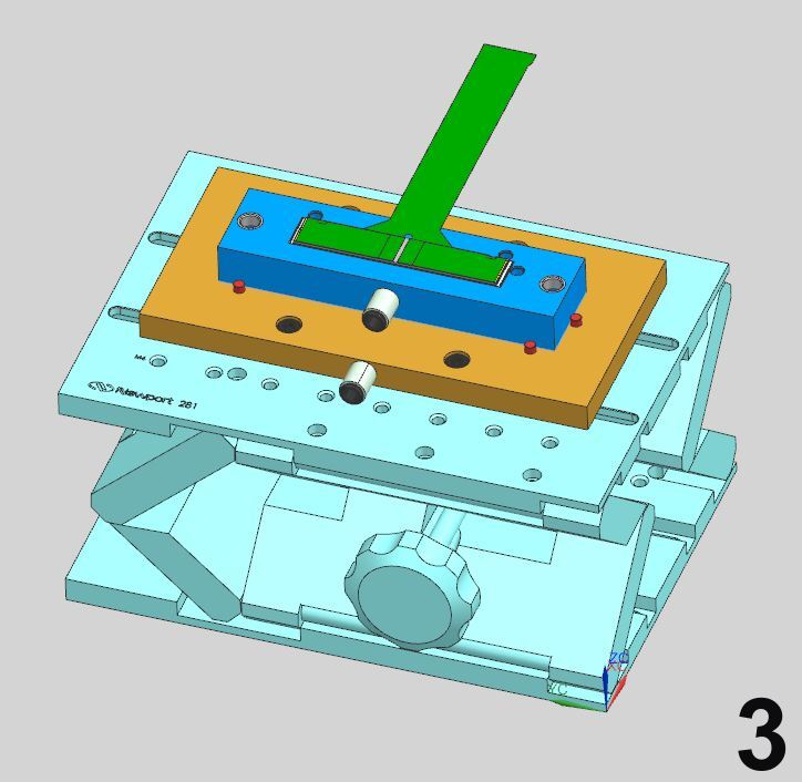
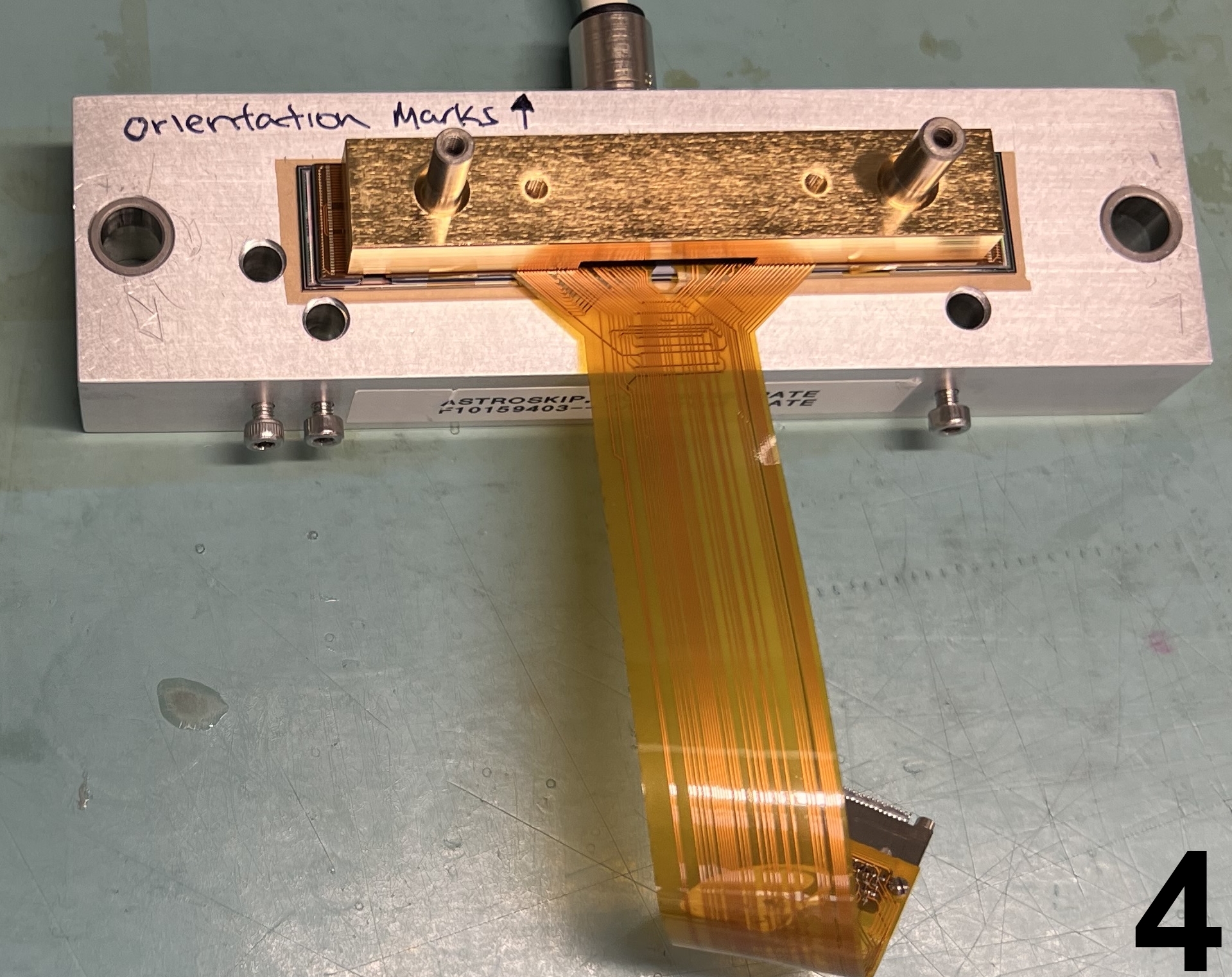
The mechanical packaging process (Fig. 4) starts by (1) attaching the flex cable to a 90.74mm 16.36mm 1.00mm silicon (Si) substrate piece. A mechanical fixture is used to align the Si substrate and a vacuum system that runs through the fixture is used to apply suction and hold the substrate in place. The flex cable is attached to the Si substrate using two pyralux sheets. The Si substrate–pyralux–flex cable assembly is cured at C for 3.5 hours under vacuum. (2) The CCD is attached to the Si substrate–flex cable assembly. Another fixture is used to align the CCD with the the Si substrate, and double-sided tape is used to secure the CCD to the Si substrate while epoxy is applied [16]. Epotek 301-2 epoxy is dispensed through a small cutout in the edge of the Si substrate near one of the corners and is allowed to fill the region between the CCD and the Si substrate. The epoxy is allowed to cure for 48 hours. (3) Wirebonding is performed between the pads on the CCD and flex cable. (4) We attach the CCD assembly to a gold-plated invar foot that serves as the structure for mounting the packaged Skipper CCDs on the focal plane. The fixture holding the CCD is placed onto the foot gluing plate; Masterbond EP21TCHT-1 epoxy is used to attach the CCD assembly and the foot and is allowed 18 to 24 hours to cure. (5) The packaged AstroSkipper is placed within an aluminium carrying box for storage and transport. The carrying box has a removable cover and is compatible with our CCD testing stations. The storage box can be directly mounted to the cold-finger plate inside the testing vacuum chambers and the storage box cover can be removed for CCD testing. To date, we have successfully packaged and tested three thick AstroSkipper CCDs at Fermilab.
4.3 Testing Stations
We have assembled two similar testing stations for characterizing the performance of the packaged AstroSkipper CCDs. The detectors are installed in closed-cycle vacuum dewars. One of the dewars has a fused silica window that can be used to illuminate the detector for optical characterization tests. The AstroSkipper carrying box attaches to an aluminium plate that is screwed to a copper cold finger. The systems are cooled by a closed-system cryogenic cooler; the temperature in our systems is maintained stable at 140K by a Laskeshore temperature controller. The readout chain consists of a second-stage flex cable, an internal dewar board (IDB), a vacuum interference board (VIB), an output dewar board (ODB), and a low-threshold acquisition (LTA) board (Section 6). The IDB allows for selecting 4 out of 16 channels for readout. Since we are testing the performance of individual detectors (each detector has four amplifiers), we select the desired amplifiers with the IDB and use a single LTA to read out a single detector. We are currently designing a second stage flex cable for Fermilab testing that will select the four channels, eliminating the IDB from the readout chain and potentially eliminating noise sources.
4.4 Detector Performance
We implement the following tests to characterize the performance of the packaged AstroSkipper CCDs: measuring the readout noise, which involves quantifying electron peaks and verifying that the readout noise behavior follows Eq. (1), and measuring the charge transfer inefficiency (CTI).
Readout noise: We measure the readout noise performance of the packaged thick AstroSkipper detectors. Similar to Drlica-Wagner, et al. (2020) [10], we see a small light leak that leads to charge collection in the overscan pixels when they are shifting into the serial register, causing the appearance of electron peaks in the overscan pixel distribution. To measure the single-sample readout noise, we use a 800-sample image, where we read out 50 rows by 3200 columns of the detector, and fit the overscan pixel distribution with a multi-Gaussian model where the single-sample readout noise is given by the standard deviation of the 0 peak. We perform the single-sample readout measurement for all of the amplifiers in the three detectors and find readout noise values ranging from to . These initial readout noise values are higher than observed in similar Skipper CCDs, which have a single-sample readout noise of [10, 6, 15]. The total readout noise in a system depends on all noise sources in the readout chain: the internal CCD readout MOS-FET transistor, interface electronics for preamplification, and data acquisition and video signal processing. Control and bias signals that can couple to the detector’s internal readout and cabling, i.e., flex cables may also contribute to the readout noise. Furthermore external noise source such as vibrations from the cryogenic cooler and or poor grounding will couple to the video signals [7]. We are using newly assembled testing chambers and currently exploring these potential noise sources to improve the noise of the testing systems. The resulting noise performance as a function of the averaged samples is shown in the left panel of Fig. 6. We see a deviation from the theoretical expectation (Eq. 1) for extensions 1, and 3 at 300 samples per pixel (extensions with best readout noise performance). Extensions 0 and 2, which have poor noise performance, deviate from the theoretical expectation for all samples per pixel. We attribute these deviations to some source of correlated noise, which causes the readout noise behavior to deviate from the theoretical model for uncorrelated measurements.
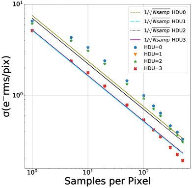

Electron counting and gain: The right plot in Fig. 10 shows the pixel distribution of a 800-sample image taken with one of the the AstroSkipper CCDs; the peaks in the distribution quantize single electrons. Single electron/photon resolution in the detector is achieved when the charge of each pixel can be precisely determined, i.e., electron-counting in Fig. 6 right panel. The gain of the entire signal video chain can be measured by the electron counting capability. The gain, which represents the relation between Analog-to-Digital-Units (ADUs) and electrons, is given by the difference of the mean values of consecutive fitted electron peaks in the pixel distribution. We measure gain values between 200 ADU/ and 221 ADU/ for all of the amplifiers in the three Skipper CCDs.
Charge Transfer Inefficiency: We measure the charge transfer inefficiency from two packaged AstroSkipper CCDs in all amplifiers, using the extended pixel edge response (EPER) [17]. We use several single-sample images, containing ; The EPER method consists of measuring the excess counts in the first overscan column resulting from CTI. This number is normalized to the total number of electrons in the last physical column and the number of horizontal charge shifts to get the final CTI value. We calculate an average CTI value, from all the amplifiers, of . We note that this measurement did not consider voltage optimizations; however, CTI is one parameter we will optimize, along with full-well capacity and readout noise.
5 DEWAR AND FOCAL PLANE
5.1 Standard SOAR Dewar
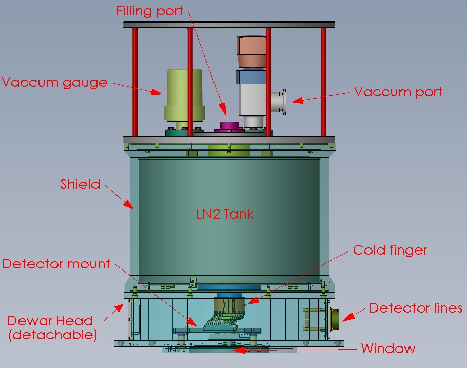
SOAR uses a standard dewar design for most of its visible instruments, which is also shared by some instruments at Cerro Tololo Inter-American Observatory (CTIO). The dewar has a single LN2 tank, and it reaches a typical vacuum on the order of Torr, with a holding time over 30 hours when full [18]. It has a molecular sieve that allows it to keep a stable vacuum for several months without the need for intervention.
Fig. 7 shows a cross section through a SOAR dewar. The LN2 tank is filled through the filling port once per day by the day crew. The dewar has an incorporated vacuum gauge that allows for both a direct view (digital screen) or remote telemetry of the current vacuum value. Surrounding the LN2 tank, there is an aluminum shield. The detector mount, located in the lower part of the dewar (“head”), is thermally connected to the LN2 tank through a copper piece attached to a coldfinger. The thermal adjustment is done by trimming some copper braids, ensuring a safe “cold storage” for the detector. The detector mount usually incorporates a heater that allows the CCDs to be kept at a prescribed operating temperature. The detector biases and clocks, as well as the video signals are passed through two 41-pin round hermetic connectors. The detector is installed in the lower part of the dewar, called the “head”, which is detachable from the main body and can be customized depending on the instrument (back focal distance, detector mount, etc.).
5.2 SIFS AstroSkipper Dewar
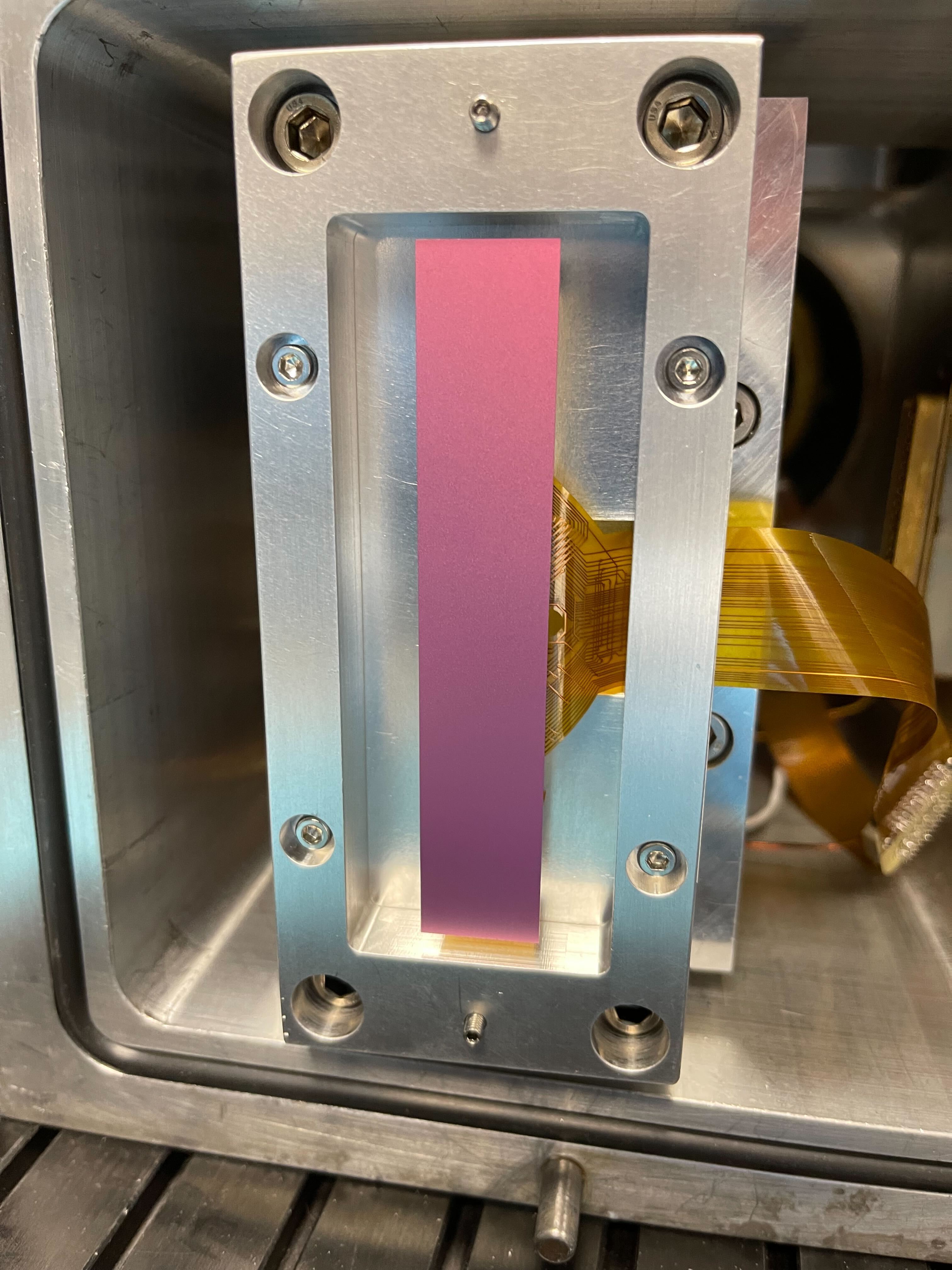
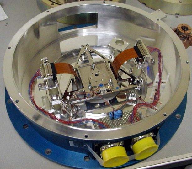
The SIFS dewar has a customized mount designed specifically for its e2v detector. Fig. 8 shows the SIFS dewar head with the current detector mount. The mount, which is the triangular aluminum piece in Fig. 8, mounts to the dewar head through three posts.
Since in SIFS the dewar is independent of the rest of the instrument, by replacing the current detector and mount with one that holds the AstroSkipper CCDs and ensuring the same spatial coverage and back focal distance, there is no need to make any modification to the instrument itself. However, given that SIFS is a production instrument and this is just a prototype, it is impossible to modify the SIFS dewar itself. Instead, we use an unfinished SOAR dewar with original parts built for the COSMOS red side (but never actually implemented), manufacture the missing pieces, and fit a spare dewar head identical to that of SIFS (this was kept in the detector laboratory for testing purposes). In this way, it will be possible to remove the current SIFS dewar and install the one with the AstroSkipper CCDs without making any mechanical change to the instrument. This will also facilitate returning to the original dewar configuration, since this operation does not take more than a couple of hours during the day.
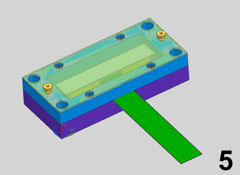
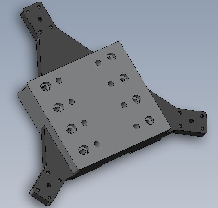
Having a dewar and a head identical to that of SIFS, all that is required is to design and fabricate a new detector mount to hold the AstroSkipper CCDs. The mount was designed at LNA and manufactured at CTIO. The CAD model is shown in Fig. 9. The mount is made of aluminum 6061 and holds four Fermilab-packaged AstroSkipper detectors using rods to place the detectors on the mount. The expected gap between detectors is expected to be , and any focal adjustment will be done with shims (the mount has no movable parts). The mount has three ears that are identical to those of the current mount, allowing it to use the same mounting holes. Special posts will be manufactured so that the mount is placed at a height that ensures the same back focal distance than the current detector. We will install two heaters and an RTD to have an appropriate temperature control. All the detector signals will be passed through the two 41-pin connectors.
6 READOUT ELECTRONICS
6.1 The LTA and Synchronized Readout Strategy
The LTA readout board was designed at Fermilab for performing the readout of the Skipper CCDs [7]. We will be using 4 LTAs to read out the 4 Skipper CCDs that will go into the SIFS Skipper CCD focal plane. The LTA is a single PC board hosting 4 video channels for readout, plus CCD bias and control. The board was designed and optimized to work with -channel, thick, high resistivity Skipper CCDs. The LTA is controlled by a Xilinx Artix XC7A200T FPGA, which sets up the programmable bias voltages/clocks, to move the charge along the CCD pixel array, video acquisition, telemetry, and data transfer from the board to the PC. The LTA software is written in C and allows for communication using UPD over IP through the computer giga-Ethernet port. The user can communicate with the LTA via terminal commands to perform board configuration, readout and telemetry requests, and sequencer uploading. The data acquisition comes in the form of images in FITS and other formats.
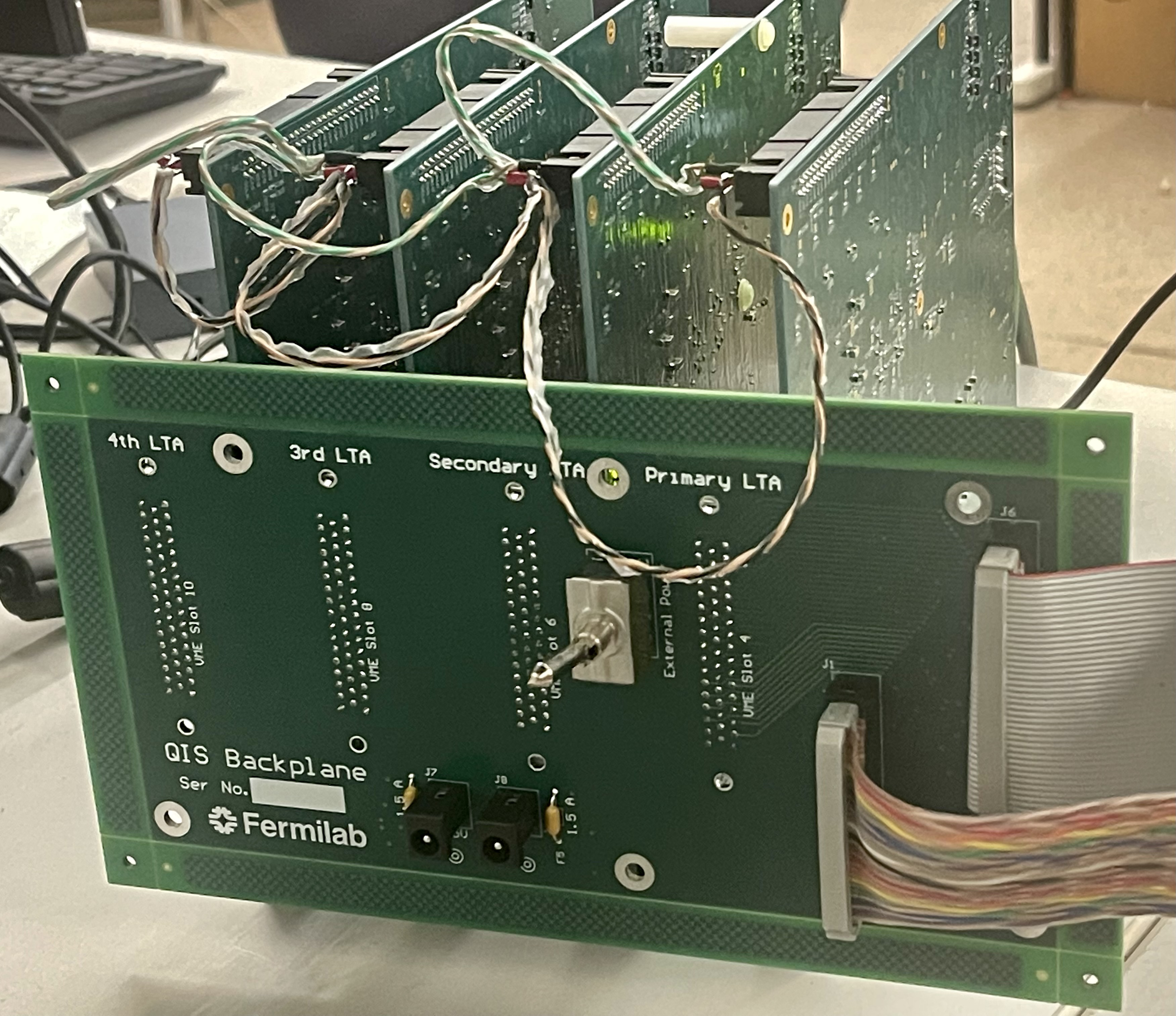
The Skipper CCD focal plane will consists of four AstroSkipper CCDs; therefore, a synchronized readout system will be needed to read out the four detectors at the same time. The LTA allows for easily scaling to several CCDs in parallel. A synchronized LTA system consists of connected boards where the “Leader” LTA provides the voltage clocks and a start signal to the LTAs in “Follower” mode; this configuration assures that all boards commence the readout sequence in parallel with synchronized clocks. Each board will be responsible for reading out one detector (4 amplifiers per detector; 16 amplifiers total). We have extensively tested the LTA synchronized readout system, consisting of four LTAs, with a set of 16-amplifier, 2k 4k detectors (Fig. 10 Left), fabricated on the same wafers as the AstroSkipper CCD. For this synchronized system (Fig. 10 Right), each of the four LTAs reads out a quadrant of the detector, containing four amplifiers; the LTAs connect to a backplane, which can provide power to the boards and distributes biases and video signals.
6.2 Readout Electronics at SOAR
6.2.1 LTA mechanical enclosure
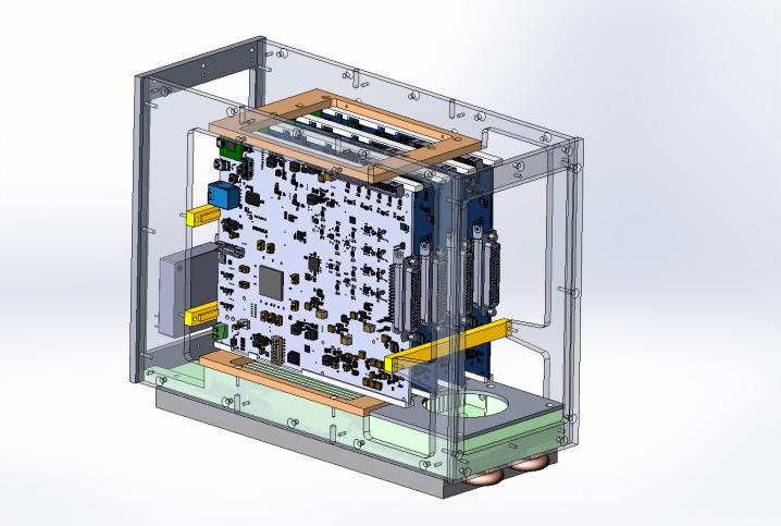
The current SIFS readout electronics is a SDSU-III controller. Given the thermal constrains, the housing is being cooled using glycol provided by the telescope facilities. The AstroSkipper CCDs, on the other hand, will be read out using 4 synchronized LTA boards. Due to the same environmental constrain, they will need to be enclosed in a glycol-cooled box. This box was designed at CTIO and is currently being manufactured. A CAD model of the box can be seen in Fig. 12. The box has a fan for air re-circulation and a heat exchanger plate cooled with glycol which was designed to dissipate at least 200W. The box also includes two 12V supplies (6 amps each) and a 5V supply, used for the preamps on the electronic box inside the dewar.
6.2.2 Electronic preamplifier board and cabling
Due to the nature of the application and the space available inside the dewar, CTIO designed a special preamplifier board that will both fit on the envelope of the dewar and provide preamplification that is more suitable for an astronomical application.
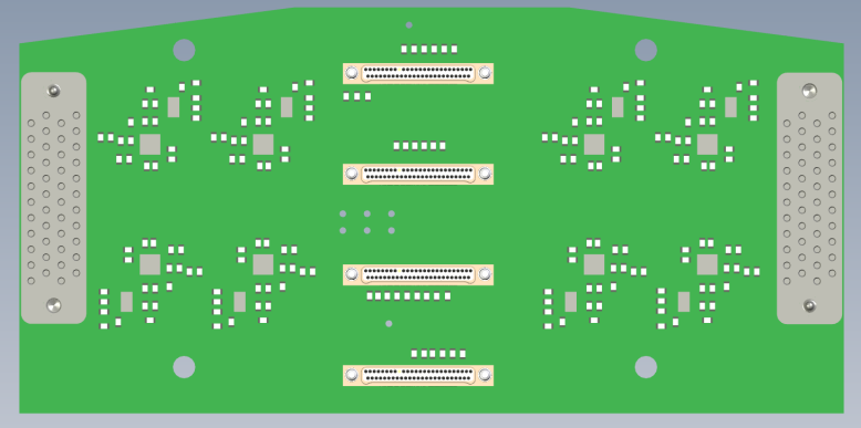
The electronic preamplifier PCB consists of a 12.49 cm 6.15 cm, eight layer, two-sided PCB board with 16 preamplifier circuits, i.e., 4 preamplifiers per AstroSkipper CCD. The preamplifier board amplifies and converts to differential the output signal from the LSJ689 JFET, which allows it to isolate the video output signal from external noise sources. Finally, the differential output signals from the preamplifier board are connected to the input amplifiers at the LTA. A CAD model of the preamplifier board can be seen in Fig. 11. Currently the preamplifier PCB board is in the component assembly and testing stage.
For a nominal dynamic range of 50000 (more suitable for astronomical applications), the end-to-end gain from the detector to the ADC is set to 32.51 . This gain give us a conversion factor of 0.48 in the ADC. Table 3 shows the simulated characteristics of the whole electronic chain from the CCD video output to the ADC input at the LTA.
| Characteristic | Value | Unit |
|---|---|---|
| Passband Gain | 30.24 | |
| Low Cut-off | 15.9 | |
| High Cut-off | 960 | |
| Total Input Referred Noise | 2.018 |
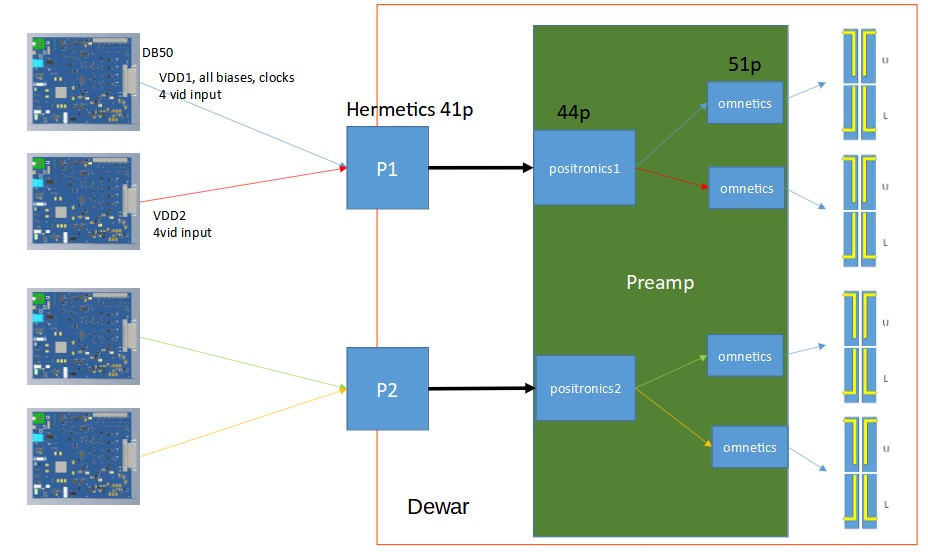
The signals in and out of the preamplifier board are handled through cable rather than a VIB. This was for simplicity and compatibility with the SOAR dewar since the 241 pin hermetics were enough to handle the signals for the 4 AstroSkipper detectors. There are two sets of cables, the internal, cryogenic ones, that take the signals from/to the preamplifier board to the hermetic connectors (inside the dewar), and another external set that takes them from the hermetics to the LTA boards inside the enclosure. The internal cables are made with 32-AWG cryogenic phosphor-bronze Lakeshore cable, due to its good combination of low resistivity (3.45 /m) and low thermal conductivity (25 W/mK) at 77K [19], using single strand for clocks and biases, and dual twisted pair ones for video signals. The external cables are single 32-AWG copper cables for biases and clocks, and 32-AWG twisted pairs for video signals. Fig. 13 shows the wiring design. Two LTAs handle two AstroSkipper detectors independently, with one hermetic servicing two AstroSkipper CCDs and its LTAs. This allows for symmetrical cables and also, if required, it would be possible to read any group of only two AstroSkipper CCDs. The biases and clocks are shared between two AstroSkipper CCDs and are provided by one LTA, except for VDD which is independent. The four LTAs will be installed on the electronics box described in Section 6.2.1.
7 Future Work
7.1 Detector Characterization
LBNL is currently processing five wafers, which includes thinning to 250 m, backside treatment, and the application of antireflective coating [12]. We will perform extensive optical characterization of these processed AstroSkipper CCDs. We plan to use an optical system, which includes a tungsten arc lamp, motorized filter wheel, monochromator, shutter, NIST-calibrated photodiode and integrating sphere. This system has been assembled and tested; we have placed the optical setup in a “dark room” to minimize the light leaks and background ambient radiation. We plan to study the full dynamic range of these detectors by constructing photon transfer curves (PTCs); PTCs will also serve as a tool to optimize the full well capacity. Furthermore, we plan to perform an absolute quantum efficiency (QE) measurement by packaging a photodiode and placing it inside the vacuum testing chamber for calibration; we have been able to do relative QE measurements on Skipper CCDs [10]. These studies will demonstrate the feasibility for using the Skipper CCD at SIFS as we expect them to retain the well-characterized performance of conventional CCDs in the optical, near infrared regimes.
7.2 Fast Readout Strategies and Optimization
The Skipper CCD’s ability to reduce readout noise through multiple non-destructive measurements of charge packets comes at the cost of increased readout times. For instance, Skipper CCD readout times for a single sample measurement with readout noise of is pix. Yet, when taking multiple non-destructive measurements of the charge in each pixel, the readout time scales as . Therefore, in applications where ultra-low noise is required, data collection can take several hours [20]. Long readout times are undesirable in astronomical observations. For nearly all astronomical applications, the exposure time and the readout time need to be optimized as a function of the signal-to-noise. Therefore, for a given astronomical observation, there is a minimum at which the signal-to-noise gain from the Skipper CCD’s reduced readout noise is overcome by the lost exposure time due to a long readout time [10]. We will explore software and firmware based strategies that can be implemented in the time frame of the installation of Skipper CCD focal plane at SIFS.
Firmware Modifications: The LTA’s FPGA firmware enables complex clock sequences; however for fast sequences, this flexibility can result in broken timing structures for time-critical clocking signals and data corruption [21]. The current readout rate for simple clock sequences such as the multiple samples per pixel readout mode is limited to kpix/sec. We have developed a new low-level LTA firmware that allows for sequence executions at a rate of Mpix/sec; there is extensive testing that needs to be completed in order to validate the detector readout noise performance running with this new firmware. Furthermore, we need to understand and remove any systematics, such as bias shifts, introduced to the data as a result of reading out fast.
Region of Interest: The Skipper CCD provides the ability to adjust the number of non-destructive measurements of charge packets on a pixel-by-pixel basis. Functionally, one can configure regions of interest (ROI) on the detector to readout out with ultra-low noise while the remaining of the detector is read out quickly with a single sample per pixel [10]. Furthermore, the number of non-destructive measurements can be chosen dynamically depending on the measured charge contained in a pixel (also called “energy of interest” in the context of energetic particle detection) [21]. The ROI technique can drastically reduced readout times since depending on the application, one might need to read out a portion of the detector with low noise. For spectroscopy, one can define a ROI to be a faint spectral line at a predetermined wavelength and read out this region with a target samples per pixel to achieve the desired noise. We plan to make this functionality more robust by designing software to target pre-determined regions of the CCD area suited for spectroscopy. Furthermore, we need to develop correction techniques to bias-correct images where the readout noise varies pixel-to-pixel. We will implement ROI at SIFS for the first time in a real observing scenario as a proof of concept.
7.3 Detector Testing at CTIO and SOAR
We will conduct extensive characterization of the performance of the four packaged, 250 thick AstroSkipper detectors at the CTIO detector’s lab to verify and compare with the results from Fermilab characterization tests. This will allow us to test for any damage of the AstroSkipper detectors during transport to Chile; furthermore, it is important to verify previous characterization results obtained at Fermilab before installing the AstroSkipper CCD focal plane at SOAR.
At CTIO detector’s lab, we will use the implemented fully-automated detector testbench, an evolution of the testbench constructed in collaboration between Fermilab and CTIO for testing DESI detectors. This testbench, described in Bonati et al. (2020) [22], is used to perform detector characterization tests at different illumination levels. The testbench uses an automated system consisting of optical hardware similar to the one we use at Fermilab for optical characterization (Section 7.1) and software that allows for data acquisition, reduction, and visualization. The automated testbench characterization sequence is divided between light and dark tests. Light tests measure low- and high-light non linearity, to evaluate the non-linearity of the detector in low-, high-light conditions, Charge Transfer Efficiency (CTE), flat-fields, for identifying cosmetic defects, and absolute quantum efficiency, to measure how many photons that arrived at the detector are effectively converted to electrons. Dark tests, performed with no light, measure the readout noise of the detector, and dark current. Test results are compared with predetermined requirements to assign a grade, i.e., mechanical, engineering, and science to the detector; a science grade-detector must have QE , cosmetics , CTI , full-well K , non-linearity , dark current /pix/h, and readout noise at 100kHz [22]. CTIO detector’s lab has a similar testing chamber to what we have at Fermilab; therefore, testing individual detectors should be possible. However, we plan to assemble the AstroSkipper CCD focal plane in the dewar and test the four synchronized AstroSkipper CCDs at CTIO detector’s lab. We will then move the working assembly and detector configuration to the SOAR telescope.
Detector characterization at SOAR will focus on validating target single-sample readout noise and readout time for observation optimization purposes. For example, we will verify that the 16-amplifiers (4 amplifiers per AstroSkipper CCD) achieve a single-sample readout noise with readout time of s per pixel ( 30s readout time for the entire detector array of four AstroSkipper CCDs). We will also target a readout noise of in min through multiple measurements of the charge in each pixel. Furthermore, we will verify the ROI capability by demonstrating that the AstroSkipper CCDs can achieve sub-electron readout noise over a fraction of the detectors’ area.
Note that the DAQ software that will be used at CTIO’s laboratory testbench, called panView[23][24], allows to hide the particulars of the detector controller, making it transparent for the callers what hardware is in use. Since the SIFS instrument at the SOAR telescope uses panView as DAQ (using an SDSU-III controller), there are no modifications of any type that will be required to the instrument software (GUI/scripts/TCS/mechanisms, etc.).
7.4 SIFS Commissioning and Installation
Commission of the Skipper CCD focal plane prototype will consists of removing the current cryostat from the bench spectrograph (Fig. 1), installing the new cryostat with the four mounted AstroSkipper CCDs, proper alignment to ensure focal distance, and installation and configuration of the readout electronics. Furthermore, we will configure detector operation modes that are optimized for observing scenarios. Detector optimization will involve developing tools to calculate and optimize the trade-off between readout noise and readout time as a function of observed wavelength, signal strength, and background level in order to determine the optimal number of non-destructive measurements per pixel. Moreover, as part of the observation configurations, we will test ROI selection for faster readout times in observational scenarios where faint spectral features are targeted at predetermined pixel locations. We will characterize detector performance in operation at the telescope; this will involve exposing the detector to different signal strengths, i.e., bright and faint spectral lines and quantify readout noise and detector cross-talk, for example. Finally, we will demonstrate stable detector performance over extended observing runs.
7.5 Planned Science Verification
In science verification, we intend to validate the performance of the Skipper CCD by targeting faint sources at blue wavelengths where the sky background is minimal and the detector readout noise contribution is important. For example, one plausible science verification target would be the study of emission lines in a population of star-forming low-surface brightness galaxies (LSBGs) detected in multi-band imaging from the Dark Energy Survey [25]. We will follow the procedure described in Greco et al. (2018) [26] to select likely star-forming LSBGs starting with the blue subpopulation and matching to UV detections in GALEX. We will then use the procedure described in Palumbo et al. (2020) [14] to extract object’s physical properties from SIFS data cubes after having selected target LSBGs. Our goal is to demonstrate that the AstroSkipper will reduce readout noise in the detector pixels corresponding to the expected spatial and spectral location of star-forming H ii regions in the targeted LSBGs. We expect to be able to recover redshifts, internal velocity dispersions, and star formation rates from the data taken with the AstroSkipper CCD focal plane at SIFS.
Acknowledgements.
This work was supported in part by Fermilab LDRD 2019.011 and LDRD 2022.053. This material is based upon work supported by the U.S. Department of Energy, Office of Science, Office of Workforce Development for Teachers and Scientists, Office of Science Graduate Student Research (SCGSR) program. The SCGSR program is administered by the Oak Ridge Institute for Science and Education for the DOE under contract number DE‐SC0014664. The work of M.B., B.C., and P.M. is supported by NOIRLab, which is managed by the Association of Universities for Research in Astronomy (AURA) under a cooperative agreement with the National Science Foundation. SIFS construction was supported by FAPESP 1999/03744-1 and Laboratório Nacional de Astrofísica (LNA/MCTI). CCD development was supported by the Lawrence Berkeley National Laboratory Director, Office of Science, of the U.S. Department of Energy under Contract No. DE-AC02-05C H11231. This manuscript has been authored by Fermi Research Alliance, LLC under Contract No. DE-AC02-07CH11359 with the U.S. Department of Energy, Office of Science, Office of High Energy Physics. The United States Government retains and the publisher, by accepting the article for publication, acknowledges that the United States Government retains a non-exclusive, paid-up, irrevocable, world-wide license to publish or reproduce the published form of this manuscript, or allow others to do so, for United States Government purposes.REFERENCES
- [1] de Oliveira, A. C., de Oliveira, L. S., Gneiding, C. D., Barbuy, B., Jones, D., Figueredo, M. V., Lépine, J. R. D., Macanhan, V. B. P., de Oliveira, J. B. C., and Taylor, K., “The SOAR integral field unit spectrograph optical design and IFU implementation,” in [Modern Technologies in Space- and Ground-based Telescopes and Instrumentation ], Atad-Ettedgui, E. and Lemke, D., eds., 7739, 1646 – 1657, International Society for Optics and Photonics, SPIE (2010).
- [2] da Silva, P., Menezes, R. B., and Steiner, J. E., “The nuclear region of NGC 613 – i. multiwavelength analysis,” Monthly Notices of the Royal Astronomical Society 492, 5121–5140 (jan 2020).
- [3] Lepine, J. R. D., de Oliveira, A. C., Figueredo, M. V., Castilho, B. V., Gneiding, C., Barbuy, B., Jones, D. J., Kanaan, A., de Oliveira, C. M., Strauss, C., Rodrigues, F., Andrade, C. R., de Oliveira, L. S., and de Oliveira, J. B., “SIFUS: SOAR integral field unit spectrograph,” in [Instrument Design and Performance for Optical/Infrared Ground-based Telescopes ], Iye, M. and Moorwood, A. F. M., eds., 4841, 1086 – 1095, International Society for Optics and Photonics, SPIE (2003).
- [4] Janesick, J. R., Elliott, T., Dingizian, A., Bredthauer, R. A., and Chandler, C. E., “New advancements in charge-coupled device technology - Sub-electron noise and 4096 4096 pixel CCDs,” SPIE 1242, 223–237 (1990).
- [5] Chandler, C. E., Bredthauer, R. A., Janesick, J. R., and Westphal, J. A., “Sub-electron noise charge-coupled devices,” in [Charge-Coupled Devices and Solid State Optical Sensors ], Blouke, M. M., ed., 1242, 238 – 251, International Society for Optics and Photonics, SPIE (1990).
- [6] Tiffenberg, J., Sofo-Haro, M., Drlica-Wagner, A., Essig, R., Guardincerri, Y., Holland, S., Volansky, T., and Yu, T.-T., “Single-electron and single-photon sensitivity with a silicon Skipper CCD,” Phys. Rev. Lett. 119(13), 131802 (2017).
- [7] Cancelo, G., Chavez, C., Chierchie, F., Estrada, J., Fernandez Moroni, G., Paolini, E. E., Sofo Haro, M., Soto, A., Stefanazzi, L., Tiffenberg, J., Treptow, K., Wilcer, N., and Zmuda, T., “Low Threshold Acquisition controller for Skipper CCDs,” IEEE 2019 Argentine Conference on Electronics (CAE) , 86–91 (2020).
- [8] Cancelo, G. I., Chavez, C., Chierchie, F., Estrada, J., Fernandez-Moroni, G., Paolini, E. E., Haro, M. S., Soto, A., Stefanazzi, L., Tiffenberg, J., Treptow, K., Wilcer, N., and Zmuda, T. J., “Low threshold acquisition controller for Skipper charge-coupled devices,” Journal of Astronomical Telescopes, Instruments, and Systems 7(1), 1 – 19 (2021).
- [9] Barak, L., Bloch, I. M., Botti, A., Cababie, M., Cancelo, G., Chaplinsky, L., Chierchie, F., Crisler, M., Drlica-Wagner, A., Essig, R., Estrada, J., Etzion, E., Moroni, G. F., Gift, D., Holland, S. E., Munagavalasa, S., Orly, A., Rodrigues, D., Singal, A., Haro, M. S., Stefanazzi, L., Tiffenberg, J., Uemura, S., Volansky, T., and and, T.-T. Y., “SENSEI: Characterization of single-electron events using a skipper charge-coupled device,” Physical Review Applied 17 (jan 2022).
- [10] Drlica-Wagner, A., Villalpando, E. M., O’Neil, J., Estrada, J., Holland, S., Kurinsky, N., Li, T., Moroni, G. F., Tiffenberg, J., and Uemura, S., “Characterization of skipper CCDs for cosmological applications,” in [X-Ray, Optical, and Infrared Detectors for Astronomy IX ], Holland, A. D. and Beletic, J., eds., 11454, 210 – 223, International Society for Optics and Photonics, SPIE (2020).
- [11] Dawson, K., Bebek, C., Emes, J., Holland, S., Jelinsky, S., Karcher, A., Kolbe, W., Palaio, N., Roe, N., Saha, J., Takasaki, K., and Wang, G., “Radiation Tolerance of Fully-Depleted P-Channel CCDs Designed for the SNAP Satellite,” IEEE Transactions on Nuclear Science 55, 1725–1735 (June 2008).
- [12] Flaugher, B. et al., “The Dark Energy Camera,” Astron. J. 150, 150 (2015).
- [13] Macanhan, V. B. P., Santoro, F. G., Gneiding, C. D., de Oliveira, A. C., Lourenço, F., Barbuy, B., Lépine, J. R. D., Figueiredo, M. V., Silva, P. F., Castilho, B., Ribeiro, F. F., de Arruda, M. V., Gutierrez, A. M., Zambretti, L. R., Rodrigues, F., Luz, H. D. P. D., and da Silva, J. M., “Mechanical design of SIFS SOAR integral field unit spectrograph,” in [Ground-based and Airborne Instrumentation for Astronomy III ], McLean, I. S., Ramsay, S. K., and Takami, H., eds., 7735, 2439 – 2445, International Society for Optics and Photonics, SPIE (2010).
- [14] Palumbo, Michael L., I., Kannappan, S. J., Frazer, E. M., Eckert, K. D., Norman, D. J., Fraga, L., Quint, B. C., Amram, P., Mendes de Oliveira, C., Bittner, A. S., Moffett, A. J., Stark, D. V., Norris, M. A., Cleaves, N. T., and Carr, D. S., “Linking compact dwarf starburst galaxies in the RESOLVE survey to downsized blue nuggets,” MNRAS 494, 4730–4750 (June 2020).
- [15] Rodrigues, D., Andersson, K., Cababie, M., Donadon, A., Botti, A., Cancelo, G., Estrada, J., Fernandez-Moroni, G., Piegaia, R., Senger, M., Sofo Haro, M., Stefanazzi, L., Tiffenberg, J., and Uemura, S., “Absolute measurement of the Fano factor using a Skipper-CCD,” arXiv e-prints , arXiv:2004.11499 (2020).
- [16] Derylo, G., Diehl, H. T., and Estrada, J., “0.250mm-thick CCD packaging for the Dark Energy Survey Camera array,” in [Society of Photo-Optical Instrumentation Engineers (SPIE) Conference Series ], Society of Photo-Optical Instrumentation Engineers (SPIE) Conference Series 6276, 627608 (2006).
- [17] Janesick, J. R., [Scientific Charge Coupled Devices ], SPIE Publications (2001).
- [18] Walker, A. R., Boccas, M., Bonati, M., Galvez, R., Martinez, M., Schurter, P., Schmidt, R. E., Ashe, M. C., Delgado, F., and Tighe, R., “SOAR Optical Imager,” in [Instrument Design and Performance for Optical/Infrared Ground-based Telescopes ], Iye, M. and Moorwood, A. F. M., eds., 4841, 286 – 294, International Society for Optics and Photonics, SPIE (2003).
- [19] Lakeshore, “Cryogenic-wire.” https://www.lakeshore.com/products/categories/specification/temperature-products/cryogenic-accessories/cryogenic-wire.
- [20] Barak, L., Bloch, I. M., Cababie, M., Cancelo, G., Chaplinsky, L., Chierchie, F., Crisler, M., Drlica-Wagner, A., Essig, R., Estrada, J., Etzion, E., Fernandez Moroni, G., Gift, D., Munagavalasa, S., Orly, A., Rodrigues, D., Singal, A., Sofo Haro, M., Stefanazzi, L., Tiffenberg, J., Uemura, S., Volansky, T., and Yu, T.-T., “SENSEI: Direct-Detection Results on sub-GeV Dark Matter from a New Skipper-CCD,” Phys. Rev. Lett. 125, 171802 (2020).
- [21] Chierchie, F., Moroni, G. F., Stefanazzi, L., Paolini, E., Tiffenberg, J., Estrada, J., Cancelo, G., and Uemura, S., “Smart readout of nondestructive image sensors with single photon-electron sensitivity,” Physical Review Letters 127 (dec 2021).
- [22] Bonati, M., Estrada, J., Castaneda, A., and Hernandez, P., “Fully automated detector testbench,” in [Software and Cyberinfrastructure for Astronomy VI ], Guzman, J. C. and Ibsen, J., eds., 11452, 290 – 302, International Society for Optics and Photonics, SPIE (2020).
- [23] Ashe, M. C., Bonati, M., and Heathcote, S., “ArcVIEW: a LabVIEW-based astronomical instrument control system,” in [Advanced Telescope and Instrumentation Control Software II ], Lewis, H., ed., 4848, 508 – 518, International Society for Optics and Photonics, SPIE (2002).
- [24] Astrophysics and space science library, eds., [Scientific Detectors for Astronomy, The beginning of a New Era ], vol. 300, ch. IV, ISPI’s software - an application of the ArcVIEW system, 427–430, Kluwer Academic Publishers (2005).
- [25] Tanoglidis, D., Drlica-Wagner, A., Wei, K., Li, T. S., Sánchez, J., Zhang, Y., Peter, A. H. G., Feldmeier-Krause, A., Prat, J., Casey, K., Palmese, A., Sánchez, C., DeRose, J., Conselice, C., Gagnon, L., Abbott, T. M. C., Aguena, M., Allam, S., Avila, S., Bechtol, K., Bertin, E., Bhargava, S., Brooks, D., Burke, D. L., Rosell, A. C., Kind, M. C., Carretero, J., Chang, C., Costanzi, M., da Costa, L. N., De Vicente, J., Desai, S., Diehl, H. T., Doel, P., Eifler, T. F., Everett, S., Evrard, A. E., Flaugher, B., Frieman, J., García-Bellido, J., Gerdes, D. W., Gruendl, R. A., Gschwend, J., Gutierrez, G., Hartley, W. G., Hollowood, D. L., Huterer, D., James, D. J., Krause, E., Kuehn, K., Kuropatkin, N., Maia, M. A. G., March, M., Marshall, J. L., Menanteau, F., Miquel, R., Ogando, R. L. C., Paz-Chinchón, F., Romer, A. K., Roodman, A., Sanchez, E., Scarpine, V., Serrano, S., Sevilla-Noarbe, I., Smith, M., Suchyta, E., Tarle, G., Thomas, D., Tucker, D. L., Walker, A. R., and DES Collaboration, “Shadows in the Dark: Low-surface-brightness Galaxies Discovered in the Dark Energy Survey,” ApJS 252, 18 (Feb. 2021).
- [26] Greco, J. P., Goulding, A. D., Greene, J. E., Strauss, M. A., Huang, S., Kim, J. H., and Komiyama, Y., “A Study of Two Diffuse Dwarf Galaxies in the Field,” ApJ 866, 112 (Oct. 2018).