Coulomb-mediated antibunching of an electron pair surfing on sound
Abstract
Electron flying qubits are envisioned as potential information link within a quantum computer [1], but also promise – alike photonic approaches [2] – a self-standing quantum processing unit [3, 4]. In contrast to its photonic counterpart, electron-quantum-optics implementations are subject to Coulomb interaction, which provide a direct route to entangle the orbital [5, 6] or spin [7, 8, 9, 10] degree of freedom. However, the controlled interaction of flying electrons at the single particle level has not yet been established experimentally. Here we report antibunching of a pair of single electrons that is synchronously shuttled through a circuit of coupled quantum rails by means of a surface acoustic wave. The in-flight partitioning process exhibits a reciprocal gating effect which allows us to ascribe the observed repulsion predominantly to Coulomb interaction. Our single-shot experiment marks an important milestone on the route to realise a controlled-phase gate for in-flight quantum manipulations.
Collision experiments provide fundamental insights into the quantum statistics of elementary particles. A prime example is the well-known Hong-Ou-Mandel (HOM) interferometer [11] where two incident particles are simultaneously scattered at a beam splitter. For the case of indistinguishable photons, they bunch due to Bose-Einstein statistics leading to an increased probability of the two particles arriving at the same detector. For colliding electrons, on the other hand, antibunching occurs because of two coexisting mechanisms – the Pauli exclusion principle and Coulomb repulsion – causing coincidental counts at the two detectors. In collision experiments performed within the two-dimensional electron gas (2DEG) in a solid-state device, it is typically assumed that Coulomb interaction is negligible due to screening by the surrounding Fermi sea and, therefore, Pauli exclusion is the dominant repulsion mechanism [12, 13, 14]. Coulomb interaction provides however a direct route for orbital entanglement [15], enabling experiments on quantum nonlocality [16, 17] and the implementation of a two-qubit gate for single flying electrons [3, 4, 7, 18]. Whether such a controlled Coulomb interaction is experimentally feasible and sufficient for orbital entanglement, however, has not yet been demonstrated.
In this work, we address this question by implementing the HOM interferometer in a depleted single-electron circuit with coupled quantum rails. In the absence of the Fermi sea along the transport paths, the screening effect is expected to be significantly reduced. We move a pair of isolated electrons from two different input ports towards a tunnel-coupled region employing the confinement potential accompanying a surface acoustic wave (SAW) [19, 20, 21]. In order to make the co-propagating electron pair collide, we tune the transmission in this coupling region such that the individual electrons are equally partitioned towards the two outputs. We synchronise the transport via triggered-sending processes [22] that we apply independently on each electron source. This control of the time delay between the two electrons allows us to contrast the full-counting statistics of the single-shot scattering events with and without interaction. Comparing our experimental results to numerical simulations, we identify the major cause of in-flight interaction and assess its applicability for orbital entanglement.
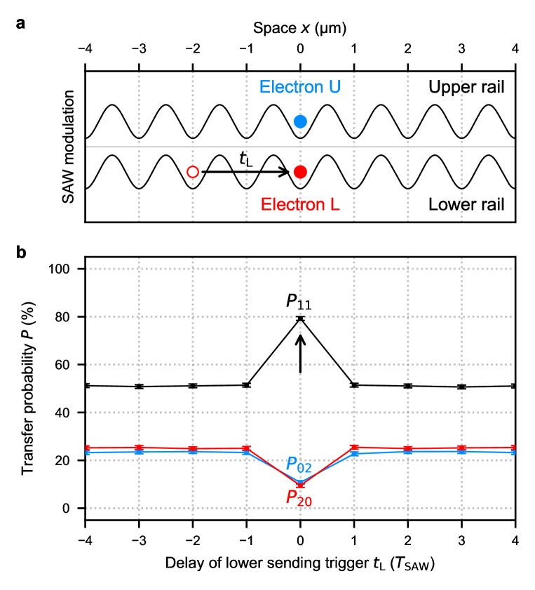
The experimental setup consists of a surface-gate-defined circuit hosting a pair of coupled quantum rails (see Fig. 1a). The SAW is emitted from a regular interdigital transducer (IDT) that is located around 1.6 mm to the left of the single-electron circuit. It travels with a speed of 2.86 m/ns and has a wavelength of 1 m. When propagating along the nanoscale device, the SAW allows shuttling of a single electron between distant quantum dots (QD) [19, 20] that are located at the respective ends of the coupled transport paths (see Fig. 1b). The presence of the electron in a QD is traced via the current flowing through a nearby quantum point contact (QPC) as a non-invasive electrometer. Enhancing the SAW potential modulation up to a peak-to-peak amplitude of meV (see Appendix A), we ensure that the transported electrons are strongly confined during flight [23]. The two injection paths of our single-electron circuit converge to a tunnel-coupled wire (TCW). Over a length of 40 m, the two quantum rails in this region are only separated by a narrow barrier that is defined via a 30-nm-wide surface gate. Before being projected to the upper (U) or lower (L) output channels, a transported electron experiences thus a flight-time of ns in this double-well potential.
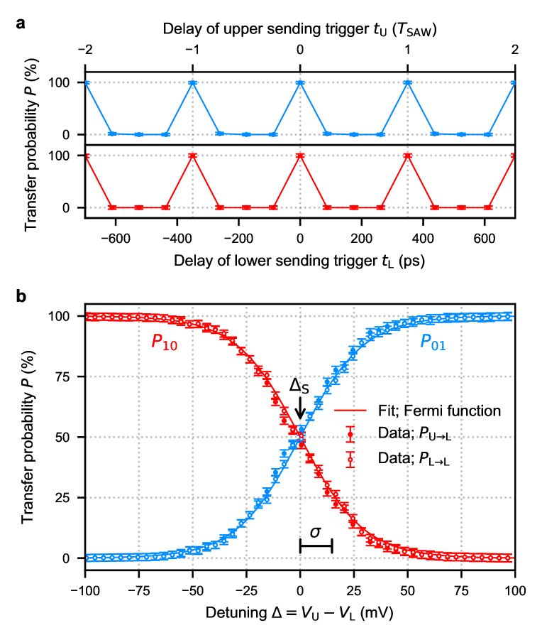
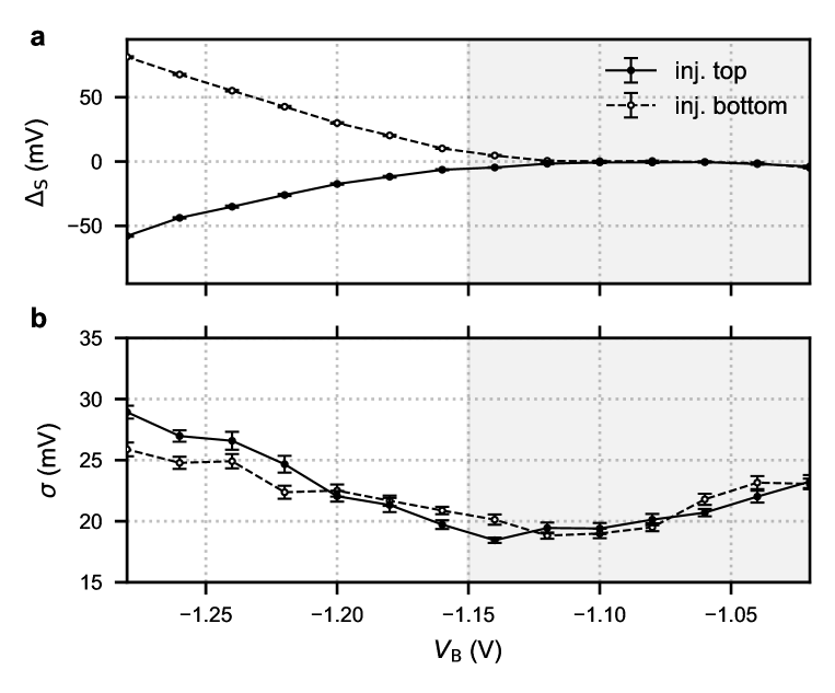
A key requirement to realise the HOM interferometer is to control the delay between individual electrons from the two source QDs. To synchronise the sending process, we apply a 90-ps voltage pulse on the plunger gate of each QD to trigger SAW-driven electron transport on demand [22]. In order to characterise the efficiency of this triggering approach, we first tune the voltages on the surface gates into a condition where the two quantum rails are decoupled. Sweeping the delay of the sending-trigger pulse with respect to the arrival time of the SAW, we observe distinct peaks in the transfer probability as shown in Fig. 2a. The spacing of the peaks coincides with the SAW period which indicates that we are able to address a specific minimum of the SAW train to transport the electron. The increase of the transfer probability from % to % for both source QDs demonstrates our ability to synchronise the electrons with high accuracy.
To implement the analog of an optical beam splitter for SAW-driven electrons [24], we investigate the partitioning of a single flying electron through the coupled quantum rails. For this purpose, we lower the barrier potential of the TCW such that the electron sent from the upper (lower) source QD can transit into the lower (upper) quantum rail with probability (). To control the in-flight partitioning, we use the side-gate voltages and to induce a detuning between the two channels. Figure 2b shows transfer probabilities for V as we detune the double-well potential within the TCW. We observe a gradual transition which follows a Fermi function:
| (1) |
with . Here, indicates the detuning for 50% transmission – that is ideally zero for a symmetric device –, and is the characteristic transition width which is related to the energy distribution of the electron. Compared to previous work [22], we observe a reduced due to mitigated excitation, which we attribute to the increased SAW confinement [23] and the improved surface-gate design at the transition region to the TCW employing realistic electrostatic potential simulations [25]. To maximise the probability of interaction, it is necessary to prepare an electron pair with similar energy, and thus equal in-flight partitioning in the coupling region. We find (see Appendix B) that such condition is satisfied for V.
Before carrying out the collision experiment, we tune the partitioning of each individual flying electron to be 50% in the coupling region via the voltages V and V. Employing the delays, and , of the sending triggers of the upper and lower source QDs, we control the relative timing between the two transported electrons as sketched in Fig. 3a. In particular, we fix the delay of the upper electron () and step the delay for the lower triggering pulse in multiples of the SAW period ( where ) in order to address different SAW minima for transport. If the electrons tunnel without experiencing the presence of the other, the probabilities at the detectors would follow a Poissonian distribution. In this case, we expect 50% for the probability to find one electron in both the upper and the lower detector, and, accordingly, and to be 25%. Figure 3b shows such a measurement of the antibunching probability as a function of the trigger delay of the electron sent from the lower source QD. We find % as expected when the two electrons are transported in different SAW minima (). As the sending triggers are synchronised () and the electron pair is thus sent within the same SAW minimum, we observe in contrast a significant increase of up to 80% resulting from the interaction between the two electrons. The distinct peak underpins our expectation that the flying electrons remain within the initially addressed SAW minimum during transport. Our observation further indicates that beyond a distance of one SAW period ( m) the interaction of the electron pair gets negligible.
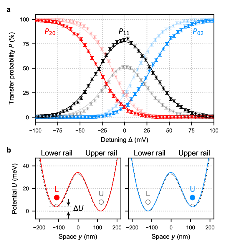
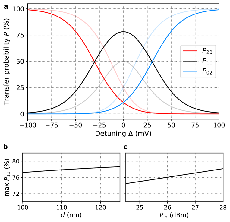
In order to investigate the nature of the antibunching effect – Pauli exclusion or Coulomb repulsion –, we perform the partitioning experiment by varying the detuning of the TCW, from the previous symmetric case to the fully detuned situation with the electron pair forced in the same channel. As reference, we first consider the non-interacting case shown in Fig. 4a by the semi-transparent data obtained with the two electrons travelling in different SAW minima (). The observed probabilities are a direct consequence of the partitioning distribution of the individual electrons shown in Fig. 2b. Since the electrons do not interact, the probability to find both electrons in the lower channel is simply the product of the single-electron cases, . Similarly, we have , and due to charge conservation. The semi-transparent lines indicate the course resulting from this non-interacting model that shows good agreement with the experimental data. As we send the two electrons synchronously within the same SAW minimum (non-transparent data), we observe a change in the functional course of and leading to a significant increase and broadening of compared to the non-interacting case.
To find out the physical effect that causes the observed in-flight partitioning of the two interacting electrons, we focus on the Coulomb potential that is experienced by one electron due to the presence of the other. We perform three-dimensional electrostatic simulations [25] taking into account the geometry and electronic properties of the presently investigated nanoscale device – see Methods. For the sake of simplicity, we consider a symmetric configuration of the surface gate voltages ( V and V). Figure 4b shows the result of an electrostatic simulation (dotted line) by adding the density of an electron-charge in the lower or upper rail. We observe that the double-well potential is tilted by the presence of the electron with an induced asymmetry of 3.7 meV, which can be reproduced by considering an effective gate-voltage detuning mV (solid line). Therefore, these numerical results indicate that the electron in the lower rail (L) experiences a potential landscape that is effectively detuned due to the presence of the electron in the upper rail (U), and vice versa.
To model the two-electron partitioning process with interaction, we include such a reciprocal electron-gating effect (parameterized by ) in the single-electron partitioning distribution (see Eq. 1) as where . In combination with the Bayes’ theorem, we derive – see Appendix C – the following expression:
| (2) |
which allows us to construct and . The solid lines shown in Fig. 4a indicate the courses of , and resulting from Eq. 2 with mV, and and extracted from the individual non-interacting partitioning data. Since the Bayesian model is solely based on electrostatics, the excellent agreement with the experimental data without adjustable parameters indicates that the Coulomb interaction is the major source of the increased antibunching probability. We further verify this conclusion by performing exact diagonalization calculations – see Appendix D – in which the long-range Coulomb repulsion is taken into account, and find a good quantitative agreement both on the increased antibunching probability and on the increased transition width.
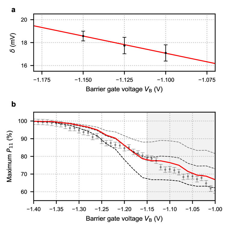
Having identified Coulomb interaction as the main cause of antibunching for a specific configuration, we now check whether this assertion also holds when the barrier potential is changed. For this purpose, we investigate the antibunching probability at a symmetric detuning () as a function of the barrier gate voltage (see Fig. 5a). Focusing on the non-interacting case (semi-transparent data), increasing the barrier height ( V) reduces the transmission of each electron to the opposite channel, leading to a gradual increase of above 50% and up to 100% when both rails are fully separated. This regime of barrier voltages with progressively decoupled rails is therefore not suitable to investigate the influence of the electron-pair interaction solely. When the electron pair is transported synchronously (black data), we observe a similar increase of in this regime starting from the optimal value of 80% discussed previously. For lower barrier heights ( V; grey area), the antibunching probability decreases gradually below 80% while the non-interacting data is saturated at 50%. To model this dependence on the barrier height, we extract the Coulomb-equivalent detuning from two-electron partitioning experiments performed at three different barrier voltages V (see Appendix E). Using a linear course of , the simulation from the Bayesian model (red) shows excellent agreement with the experimental data. The quantitative comparison indicates that Coulomb interaction is dominant for a wide range of barrier voltages.
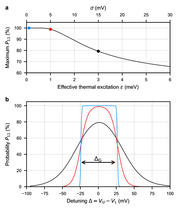
Next, we address the question of what limits the maximum observed antibunching probability at %. A possible explanation could be the occupation of excited states by the flying electrons [22]. If their energy overcomes the Coulomb repulsion, is expected to be reduced. To check this possibility, we numerically investigate the effect of excitation in the antibunching process using the Bayesian model – see Appendix F. We find that is expected to exceed 99% if the effective thermal excitation of the electron is reduced from the present 3 meV to below 1 meV.
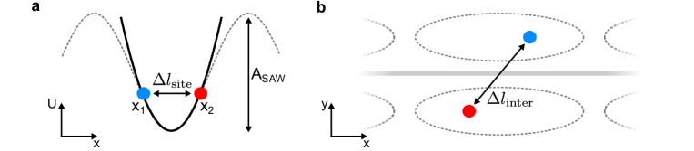
For the implementation of the two-qubit gate with flying electrons [7, 8, 26], let us estimate the extent of the reciprocal phase shift, , induced on the wavefunctions of the electron pair after an interaction time . The energy due to the Coulomb interaction is represented here as where is the distance between the two electrons, is the vacuum permittivity and is the dielectric constant of GaAs. From potential simulations, we extract a distance of nm, which gives a Coulomb energy meV. Considering the SAW velocity m/ns, we expect a phase rotation (Bell state formation) over a propagation distance nm. This estimation shows that in-flight Coulomb interaction within a TCW introduces a significant reciprocal phase shift capable of entangling the orbits in a SAW-driven single-electron circuit.
In conclusion, we have demonstrated the controlled interaction between two single flying electrons transported by sound. This has been achieved through the implementation of the HOM interferometer with a circuit of coupled quantum rails. Synchronising the transport of a pair of individual electrons, we witnessed single-shot events of fermionic antibunching. To address the underlying mechanism, we performed quantitative electrostatic simulations, and observed a reciprocal electron-gating effect. Developing a Bayesian model, which contains no adjustable parameter, we showed quantitative agreement with the entire set of two-electron collision data. This provides strong evidence that the observed antibunching is mediated by Coulomb repulsion. Further estimating the strength of this Coulomb interaction, we highlight that it is more than sufficient for the formation of a fully entangled Bell state. Combining this controlled interaction with novel, scalable single-electron-transport techniques [27], our results set an important milestone towards the implementation of the controlled-phase gate for SAW-driven flying electron qubits.
Methods
SAW transducer. The employed IDT consists of 111 cells of period m. The resonance frequency is GHz at cryogenic temperatures. To reduce internal reflections at resonance, we employ a double-electrode pattern for the transducers. The surface electrodes of the IDTs are fabricated using standard electron-beam lithography with successive thin-film evaporation (Ti 3 nm, Al 27 nm) on GaAs/AlGaAs heterostructure. The transducer has an aperture of 30 m with the SAW propagation direction along . For single-electron transport, we employ an input signal at the resonance frequency with a duration of 50 ns. To achieve strong SAW confinement, the input signal for SAW formation is enhanced by a high-power amplifier (ZHL-4W-422+; +25 dB) prior injection.
Electron-transport experiments. We use a Si-modulation-doped GaAs/AlGaAs heterostructure grown by molecular beam epitaxy (MBE). The two-dimensional electron gas (2DEG) is located 110 nm below the surface, with an electron density of and a mobility of . Metallic surface gates (Ti 3 nm, Au 14 nm) define the nanostructures. The experiment is performed at a temperature of about 20 mK in a dilution refrigerator. At low temperatures, the 2DEG below the transport channels and the QDs are completely depleted via a set of negative voltages applied on the surface gates. To enable triggering of the sending process, the plunger gate of each source QD is connected to a broadband bias tee (SHF AG; 20 kHz to 40 GHz).
Synchronisation between SAW emission and triggered sending process. We employ two dual-channel arbitrary waveform generators (AWG, Keysight M8195A) synchronised via an synchronisation unit (Keysight M8197A) for the antibunching experiments. A small jitter of ps between the AWG channels allows to control precisely the timing between SAW emission and the triggered sending process at each QD.
Potential simulations. The simulations are performed with the commercial Poisson solver nextnano [28]. We define a three-dimensional structure with realistic heterostructure layers and gate geometries where the corresponding materials’ properties are taken into account. In our electrostatic model, a metallic gate is expressed as a Schottky barrier [25, 29]. On the free surface, a layer of surface charges simulates the Fermi-level-pinning effect that is well-known in GaAs substrates [30]. Using one-dimensional simulations, we first calibrate the dopant concentration with a surface gate such that it reproduces the 2DEG density at the interface of GaAs and AlGaAs. We then adjust similarly the surface charges in the absence of the gate. The presence of an electron in one side of the rail is emulated by inserting the charge of an electron in a volume of nm, nm and nm, where () is parallel (perpendicular) to the SAW propagation direction, and is the growth direction of the heterostructure.
Acknowledgements.
We acknowledge fruitful discussions with Vyacheslavs Kashcheyevs and Elina Pavlovska. J.W. acknowledges the European Union’s Horizon 2020 research and innovation program under the Marie Skłodowska-Curie grant agreement No 754303. A.R. acknowledges financial support from ANR-21-CMAQ-0003, France 2030, project QuantForm-UGA. T.K. and S.T. acknowledge financial support from JSPS KAKENHI Grant Number 20H02559. W.P., J.S., and H.-S.S. acknowledge support from Korea NRF via the SRC Center for Quantum Coherence in Condensed Matter (Grant No. 2016R1A5A1008184). C.B. acknowledges financial support from the French Agence Nationale de la Recherche (ANR), project QUABS ANR-21-CE47-0013-01. This project has received funding from the European Union’s H2020 research and innovation program under grant agreement No 862683 ”UltraFastNano”.Appendix A Estimation of SAW amplitude
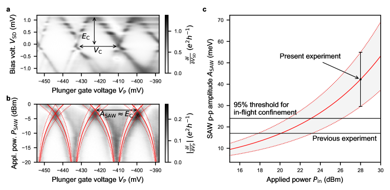
In order to investigate how the input RF power applied on the IDT relates to the SAW peak-to-peak amplitude , we measure the SAW-induced modulation of Coulomb-blockade resonances of a QD. For this purpose, we polarise the surface gates such that the QD is not depleted, and apply a bias voltage across the two leads. Varying as a function of the plunger gate voltage , we measure the conductance across the QD and obtain Coulomb diamonds as shown in Fig. S1a. This data allows us to extract the quantum dot’s charging energy and the voltage spacing between Coulomb-blockade peaks. The voltage-to-energy conversion factor is thus eV/V. Knowing , we can now deduce the SAW amplitude from a given input power via the relation:
| (3) |
where is a fit parameter accounting for power losses. is determined by comparison of Eq. 3 to the SAW-induced broadening of the Coulomb-blockade resonances. Figure S1b shows a conductance measurement as function of and for V. The data shows Coulomb-blockade peaks that broaden according to Eq. 3 with dBm as indicated by the solid lines (the dashed lines represent the error margin). Considering the here-employed input power of dBm, we extrapolate an amplitude of meV. This value lies beyond the amplitude meV reported from our previous device of coupled quantum rails [22] (lower horizontal line) which indicates that we have successfully improved the SAW confinement. To estimate if the transported electron would stay within a SAW minimum, we compare the present with the 95% confinement threshold of meV that was deduced from time-of-flight measurements along a straight quantum rail [23] (upper horizontal line). Our results indicate that the employed SAW power is strong enough to ensure in-flight confinement.
Appendix B Barrier dependence of single-electron partitioning
The partitioning data from a single electron follows a Fermi function (see Eq. 1) with a half-transmission detuning and a characteristic transition width . Figure S2a shows the evolution of as a function of the barrier-gate voltage for an electron sent from the upper (solid line) or lower (dashed line) source QD. For a large barrier height ( V), an asymmetric polarisation of the channel gates () is required to achieve 50% transmission. Comparing in-flight partitioning data from an individual electron injected from each source QD, we observe that converges gradually to a matching value when becomes more positive (lower barrier). The course of the transition width for both injection sides shows identical behaviour (see Fig. S2b). Since is related to the energy state of the partitioned electron, we find a minimal excitation for between V and -1.05 V.
Appendix C Bayesian model of in-flight partitioning mediated by Coulomb interaction
In the following, we employ Bayesian probability calculus to derive the two-electron collision probabilities , and from the single-electron-partitioning data for . Here, a transported electron enters from the input and exits at the output . In the case of two transported electrons, the probability to find both electrons in L can be defined via the joined probability
| (4) |
where is the conditional probability to find the electron sent from L at the exit L when electron U is present in channel L, and is the probability to find electron U in channel L independent on the location of electron L.
Expressing and via the Bayes’ theorem , and knowing due to charge conservation, we derive as:
| (5) |
Note that here does not need to be equivalent to the single-electron case due to the mutual influence between the electrons.
Let us first focus on the non-interacting case where the two electrons do not influence each other. For two independent events, the conditional probability satisfies . Applying this relation to equations 4 and 5, we obtain
| (6) |
that follows the Poisson binomial distribution.
In the interacting case, the presence of electron U influences L, and vice versa. For the presently studied experimental configuration, our potential simulations indicate that the Coulomb potential of electron U effectively detunes the potential landscape that is observed by L. The effect is equivalent to an effective voltage detuning on the surface gates by . Including this Coulomb interaction, we find:
| (7) | ||||
| (8) |
Similarly, the influence of electron L on electron U is expressed as
| (9) | ||||
| (10) |
Following the same procedure, we can construct and from
| (12) | ||||
| (13) |
Appendix D Exact diagonalization for transfer probabilities
Here we calculate the two-electron transfer probabilities based on the exact diagonalization method, in which the potential shape of the moving QDs induced by the SAW train, the Coulomb interaction between electrons, and an ensemble described by an effective temperature are taken into account. The results are in qualitatively good agreement with the experimental data of the transfer probabilities as a function of the detuning , the input power for SAW generation, and the barrier gate voltage . This supports that the experimental findings of the antibunching behavior originate from Coulomb interaction.
In this model, we consider a system with two electrons confined in a two dimensional potential where () corresponds to the parallel (perpendicular) direction with respect to the transport channel. is the confinement potential along the SAW propagation direction which we define as
| (14) |
where is the SAW period, and is the peak-to-peak SAW amplitude determined by the input power (see Eq. 3). We derive accordingly the SAW confinement energy using the Taylor expansion of Eq. 14 at the local minimum as
| (15) |
where is the effective electron mass in GaAs and meV is the peak-to-peak amplitude at dBm. For the experimental condition of dBm, we estimate meV.
On the other hand, describes the double-QD potential generated by a single minimum of the SAW train and the barrier gate voltage . This potential along the transverse direction is modelled, following Ref. [31], as
| (16) |
where corresponds to the single-particle level spacing in the transverse direction , is the distance between the two QDs, and the detuning combined with the conversion factor determines the asymmetry of this double-well potential. From electrostatic simulations (see Methods) using experimental conditions ( V and V), we extract meV and nm.
To include the interaction between the electron pair, we consider the Coulomb energy
| (17) |
Here, is the distance between the electrons, is the dielectric constant of GaAs, is the vacuum permittivity, is the electron charge, and is the width of the quantum well that confines the two-dimensional electron gas in direction. Considering the quantum-well confinement width, we choose nm.
Next, we define the Hamiltonian for such a system of two interacting electrons as , where are the momentum in and direction, respectively, of electron and . To solve the Hamiltonian, we convert the two dimensional continuous space into a rectangular discrete lattice, and apply the exact diagonalization method. We use a grid of with lattice constants nm and nm. Note that and are shorter than the characteristic length scale for the QDs, and , respectively. Here, is determined by Eq. 14. To reduce computational costs in calculating two-electron eigenstates, we discard single-particle basis states whose energy is higher than , where is the Boltzmann constant and is the effective temperature discussed later. Under these conditions, the calculated probabilities are converged within 1% error when decreasing , or the number of truncated states.
To better describe the experimental condition, we include an effective thermal temperature in the system to represent the nonequilibrium state due to nonadiabatic excitations generated during the electron transport [22]. Note that is different from the electron temperature of the experiment. For this purpose, we construct a thermal ensemble by using the eigenstates of the Hamiltonian obtained by the exact diagonalization and the thermal Boltzmann factor. The density operator of the ensemble is written as by considering that, for the two-electron spin state, there are 25% and 75% of spin singlet and triplet in the ensemble, respectively. The density operators and for the spin singlet and the spin triplet have the form of , where and are the -th eigenenergy and eigenstates of the spin singlet/triplet case obtained from the exact diagonalization, is the Boltzmann factor, and corresponds to the partition function.
Using the thermal ensemble , we compute the transfer probabilities of the two electrons by using
| (18) |
| (19) |
| (20) |
where is the transverse directional coordinate of electron , is reference location at the top of the tunnel barrier between the two QDs, with () is the projector onto the states of electron in the upper (lower) QD. We also compute the transfer probabilities and of a single electron by solving the Hamiltonian .
Let us now reproduce the two-electron partitioning data shown in Fig. 4a of the main text. Choosing an effective temperature of meV and a conversion factor of eV/V, we find that the computed transfer probabilities , and (with varying the detuning ) in Fig. S3a well reproduce the experimental data. These numerical results support the conclusion that Coulomb repulsion is the dominant mechanism in the observed antibunching. We note that the chosen parameters are of the same order of magnitude with the effective thermal excitation energy meV and the conversion factor eV/V estimated in Appendix F. This implies that our equilibrium state ensemble with the effective temperature and the Boltzmann factor imitates well the non-adiabatic excitations in the non-equilibrium situation of our experiment.
Furthermore, knowing that this model considers the exact confinement potential of the double-well potential, we can relate to the balance between the on-site Coulomb energy within one QD and the inter-dot Coulomb energy between the two moving QDs. In particular, if the on-site energy is larger than the inter-dot energy, having one electron on each QD is thus the favourable state, which results in an increase of .
The dependencies of the calculated transfer probabilities on the barrier gate voltage and the input power shown in Fig. S3b and S3c also provide deeper understanding of the experimental findings shown in Fig. 5a of the main text and in Fig. S6a, respectively. For instance, applying a more negative – which is equivalent to an increase of the distance between the two electrons – reduces the inter-dot energy, resulting in an enhancement of (see Fig. S3b). A stronger SAW amplitude – controlled by the input power – has a similar effect. In this case, the on-site Coulomb energy becomes larger in the modified potential profile, leading as well to an increase in (see Fig. S3c).
In summary, the good agreement between the results from the exact diagonalization method and the experimental data provides further evidence of the dominant role of Coulomb interaction in our system.
Appendix E Effective detuning dependence on barrier height
To investigate the effect of the barrier height in the TCW, we analyse the in-flight-partitioning data of two electrons that are sent simultaneously from the upper and lower source QDs. Figure S4a shows the effective detuning extracted from the partitioning data for three different barrier-gate voltages . The red line shows a linear fit providing for the Bayesian model applied for Fig. 5 in the main text. Figure S4b shows simulations of the maximum antibunching probability using the Bayesian model as a function of . The data points from experiment are shown as reference. Note that in the simulations and are taken from single-electron partitioning measurements, so that is the only free parameter. Assuming a constant (solid lines), the simulated results either over- or under-estimate . Using in the contrary the dependency extracted from a linear square fit from Fig. S4a (red line), the model shows a remarkable agreement over the whole voltage range.
Appendix F Antibunching dependency on effective thermal excitation
In the following we present a predictive investigation of the Coulomb-related antibunching rate by evaluating the Bayesian model assuming reduced excitation of the flying electrons. Figure S5a shows the maximum as a function of the single-electron partitioning width . We express as an effective thermal excitation where the gate alpha factor is extracted from a fit by assuming an exponential distribution [22]. We find that by reducing the current excitation by a factor of 3, the antibunching rate is beyond 99%. Comparing the simulated course of – see Fig. S5b –, we expect a narrowing of the distribution for smaller excitation. The saturation to 100% represents the condition where the Coulomb-mediated antibunching is robust against small variations in the gate detuning .
Appendix G The role of SAW confinement
In the following we investigate the influence of SAW confinement amplitude on the antibunching process. Figure S6a shows the excess in antibunching probability extracted from the two-electron partitioning data for several applied input power on the transducer. We observe two regimes distinguished by a change in the slope around dBm. Below this value, we know from the SAW amplitude calibration (see Fig. S1c) that the SAW confinement is not strong enough to avoid electron tunneling to subsequent minima. For the region above the 95% threshold for in-flight confinement [23], gradually increases with SAW power. A possible explanation is that, as increases, the charging energy within each moving QD becomes larger, and thus overcoming the effective thermal excitation of the electrons.
To get a better understanding, we use the Bayesian model and extract the potential detuning as shown in Fig. S6b. We observe that the course of is similar to . From previous investigations, we know that also depends on the barrier height via . While controls mainly the coupling between the quantum rails that could affect the inter-dot energy – we denote it as –, changes the confinement potential within each moving QD, i.e. on-site energy . These results suggest that is a balance between and .
To check whether this hypothesis is valid, let us assume that the effective detuning is
| (21) |
with as the conversion factor from V to eV.
Let us first estimate the on-site energy . Since the confinement energy meV along the SAW propagation direction () is smaller than the confinement energy meV along the traversal direction () for the experimental conditions – see Appendix D –, we expect that the two-electron interaction is more sensitive to than . Approximating the confinement along the direction as a parabolic potential (see Fig. S7a) and ignoring its dependency on , we can write as
| (22) |
Here, meV/nm is the Coulomb repulsion constant, is the elementary charge, is the vacuum permitivity, is the dielectric constant of GaAs, denotes for the electron effective mass in GaAs, is the parabolic confinement frequency, is the position of the electron , and corresponds to the unscreened Coulomb energy
| (23) |
Expressing Eq. 22 in terms of the on-site separation , we find via that the lowest energy of the system is
| (24) |
at the optimum distance of
| (25) |
If only few electrons are present, the ground state of the system found via this classical approach is equivalent to solving the quantum Hamiltonian [32].
Substituting from Eq. 15 in Eq. 22, we reach to the final relation
| (26) |
For the maximum applied power dBm, two electrons occupying the same moving QD would be separated by nm which results in meV.
Let us now estimate via the inter-dot distance as depicted in Fig. S7b. In the limiting case of unscreened Coulomb repulsion, the energy is simply
| (27) |
Since the co-propagating electrons have a separation nm, we estimate meV. Note that owing to , the electron pair tends to occupy different moving QDs, and hence the observation of the Coulomb-induced antibunching effect.
Having expressed as a function of the input SAW power , we employ the equations 21 and 26 to reproduce the experimental data shown in Fig. S6b where is the only fitting parameter. Using eV/V, our estimation (red line) shows a good agreement with the extracted detuning . These results confirm our expectation that the SAW amplitude modifies the on-site energy, and thus the antibunching probability.
References
- DiVincenzo [2000] D. P. DiVincenzo, The physical implementation of quantum computation, Fortschritte der Physik 48, 771 (2000).
- O'Brien et al. [2009] J. L. O'Brien, A. Furusawa, and J. Vučković, Photonic quantum technologies, Nature Photonics 3, 687 (2009).
- Bäuerle et al. [2018] C. Bäuerle, D. C. Glattli, T. Meunier, F. Portier, P. Roche, P. Roulleau, S. Takada, and X. Waintal, Coherent control of single electrons: a review of current progress, Reports on Progress in Physics 81, 056503 (2018).
- Edlbauer et al. [2022] H. Edlbauer, J. Wang, T. Crozes, P. Perrier, S. Ouacel, C. Geffroy, G. Georgiou, E. Chatzikyriakou, A. Lacerda-Santos, X. Waintal, D. C. Glattli, P. Roulleau, J. Nath, M. Kataoka, J. Splettstoesser, M. Acciai, M. C. da Silva Figueira, K. Öztas, A. Trellakis, T. Grange, O. M. Yevtushenko, S. Birner, and C. Bäuerle, Semiconductor-based electron flying qubits: review on recent progress accelerated by numerical modelling, EPJ Quantum Technology 9, 10.1140/epjqt/s40507-022-00139-w (2022).
- Kang [2007] K. Kang, Electronic mach-zehnder quantum eraser, Physical Review B 75, 125326 (2007).
- Weisz et al. [2014] E. Weisz, H. K. Choi, I. Sivan, M. Heiblum, Y. Gefen, D. Mahalu, and V. Umansky, An electronic quantum eraser, Science 344, 1363 (2014).
- Barnes et al. [2000] C. H. W. Barnes, J. M. Shilton, and A. M. Robinson, Quantum computation using electrons trapped by surface acoustic waves, Physical Review B 62, 8410 (2000).
- Lepage et al. [2020] H. V. Lepage, A. A. Lasek, D. R. M. Arvidsson-Shukur, and C. H. W. Barnes, Entanglement generation via power-of-swap operations between dynamic electron-spin qubits, Physical Review A 101, 022329 (2020).
- Jadot et al. [2021] B. Jadot, P.-A. Mortemousque, E. Chanrion, V. Thiney, A. Ludwig, A. D. Wieck, M. Urdampilleta, C. Bäuerle, and T. Meunier, Distant spin entanglement via fast and coherent electron shuttling, Nature Nanotechnology 16, 570 (2021).
- Choquer et al. [2022] M. Choquer, M. Weis, E. D. S. Nysten, M. Lienhart, P. Machnikowski, D. Wigger, H. J. Krenner, and G. Moody, Quantum control of optically active artificial atoms with surface acoustic waves, IEEE Transactions on Quantum Engineering , 1 (2022).
- Hong et al. [1987] C. K. Hong, Z. Y. Ou, and L. Mandel, Measurement of subpicosecond time intervals between two photons by interference, Physical Review Letters 59, 2044 (1987).
- Liu et al. [1998] R. C. Liu, B. Odom, Y. Yamamoto, and S. Tarucha, Quantum interference in electron collision, Nature 391, 263 (1998).
- Dubois et al. [2013] J. Dubois, T. Jullien, F. Portier, P. Roche, A. Cavanna, Y. Jin, W. Wegscheider, P. Roulleau, and D. C. Glattli, Minimal-excitation states for electron quantum optics using levitons, Nature 502, 659 (2013).
- Bocquillon et al. [2013] E. Bocquillon, V. Freulon, J.-M. Berroir, P. Degiovanni, B. Plaçais, A. Cavanna, Y. Jin, and G. Fève, Coherence and indistinguishability of single electrons emitted by independent sources, Science 339, 1054 (2013).
- Vyshnevyy et al. [2013] A. A. Vyshnevyy, A. V. Lebedev, G. B. Lesovik, and G. Blatter, Two-particle entanglement in capacitively coupled mach-zehnder interferometers, Physical Review B 87, 165302 (2013).
- Bell [1964] J. S. Bell, On the einstein podolsky rosen paradox, Physics Physique Fizika 1, 195 (1964).
- Aspect et al. [1982] A. Aspect, J. Dalibard, and G. Roger, Experimental test of bell's inequalities using time- varying analyzers, Physical Review Letters 49, 1804 (1982).
- Ionicioiu et al. [2001] R. Ionicioiu, G. Amaratunga, and F. Udrea, Quantum computation with ballistic electrons, International Journal of Modern Physics B 15, 125 (2001).
- Hermelin et al. [2011] S. Hermelin, S. Takada, M. Yamamoto, S. Tarucha, A. D. Wieck, L. Saminadayar, C. Bäuerle, and T. Meunier, Electrons surfing on a sound wave as a platform for quantum optics with flying electrons, Nature 477, 435 (2011).
- McNeil et al. [2011] R. P. G. McNeil, M. Kataoka, C. J. B. Ford, C. H. W. Barnes, D. Anderson, G. A. C. Jones, I. Farrer, and D. A. Ritchie, On-demand single-electron transfer between distant quantum dots, Nature 477, 439 (2011).
- Delsing et al. [2019] P. Delsing, A. N. Cleland, M. J. A. Schuetz, J. Knörzer, G. Giedke, J. I. Cirac, K. Srinivasan, M. Wu, K. C. Balram, C. Bäuerle, T. Meunier, C. J. B. Ford, P. V. Santos, E. Cerda-Méndez, H. Wang, H. J. Krenner, E. D. S. Nysten, M. Weiß, G. R. Nash, L. Thevenard, C. Gourdon, P. Rovillain, M. Marangolo, J.-Y. Duquesne, G. Fischerauer, W. Ruile, A. Reiner, B. Paschke, D. Denysenko, D. Volkmer, A. Wixforth, H. Bruus, M. Wiklund, J. Reboud, J. M. Cooper, Y. Fu, M. S. Brugger, F. Rehfeldt, and C. Westerhausen, The 2019 surface acoustic waves roadmap, Journal of Physics D: Applied Physics 52, 353001 (2019).
- Takada et al. [2019] S. Takada, H. Edlbauer, H. V. Lepage, J. Wang, P.-A. Mortemousque, G. Georgiou, C. H. W. Barnes, C. J. B. Ford, M. Yuan, P. V. Santos, X. Waintal, A. Ludwig, A. D. Wieck, M. Urdampilleta, T. Meunier, and C. Bäuerle, Sound-driven single-electron transfer in a circuit of coupled quantum rails, Nature Communications 10, 10.1038/s41467-019-12514-w (2019).
- Edlbauer et al. [2021] H. Edlbauer, J. Wang, S. Ota, A. Richard, B. Jadot, P.-A. Mortemousque, Y. Okazaki, S. Nakamura, T. Kodera, N.-H. Kaneko, A. Ludwig, A. D. Wieck, M. Urdampilleta, T. Meunier, C. Bäuerle, and S. Takada, In-flight distribution of an electron within a surface acoustic wave, Applied Physics Letters 119, 114004 (2021).
- Ito et al. [2021] R. Ito, S. Takada, A. Ludwig, A. Wieck, S. Tarucha, and M. Yamamoto, Coherent beam splitting of flying electrons driven by a surface acoustic wave, Physical Review Letters 126, 070501 (2021).
- Chatzikyriakou et al. [2022] E. Chatzikyriakou, J. Wang, L. Mazzella, A. Lacerda-Santos, M. C. d. S. Figueira, A. Trellakis, S. Birner, T. Grange, C. Bäuerle, and X. Waintal, Unveiling the charge distribution of a gaas-based nanoelectronic device: A large experimental data-set approach (2022).
- Helgers et al. [2022] P. L. J. Helgers, J. A. H. Stotz, H. Sanada, Y. Kunihashi, K. Biermann, and P. V. Santos, Flying electron spin control gates, Nature Communications 13, 10.1038/s41467-022-32807-x (2022).
- Wang et al. [2022] J. Wang, S. Ota, H. Edlbauer, B. Jadot, P.-A. Mortemousque, A. Richard, Y. Okazaki, S. Nakamura, A. Ludwig, A. D. Wieck, M. Urdampilleta, T. Meunier, T. Kodera, N.-H. Kaneko, S. Takada, and C. Bäuerle, Generation of a single-cycle acoustic pulse: A scalable solution for transport in single-electron circuits, Physical Review X 12, 031035 (2022).
- Birner et al. [2007] S. Birner, T. Zibold, T. Andlauer, T. Kubis, M. Sabathil, A. Trellakis, and P. Vogl, nextnano: General purpose 3-d simulations, IEEE Transactions on Electron Devices 54, 2137 (2007).
- Hou et al. [2018] H. Hou, Y. Chung, G. Rughoobur, T. K. Hsiao, A. Nasir, A. J. Flewitt, J. P. Griffiths, I. Farrer, D. A. Ritchie, and C. J. B. Ford, Experimental verification of electrostatic boundary conditions in gate-patterned quantum devices, Journal of Physics D: Applied Physics 51, 244004 (2018).
- Sze and Ng [2006] S. Sze and K. K. Ng, Physics of Semiconductor Devices (John Wiley & Sons, Inc., 2006).
- Burkard et al. [1999] G. Burkard, D. Loss, and D. P. DiVincenzo, Coupled quantum dots as quantum gates, Physical Review B 59, 2070 (1999).
- Ciftja [2009] O. Ciftja, Classical behavior of few-electron parabolic quantum dots, Physica B: Condensed Matter 404, 1629 (2009).