Tunable quantum dots from atomically precise graphene nanoribbons using a multi-gate architecture
These authors contributed equally to this work. \alsoaffiliationDepartment of Physics, University of Basel, 4056 Basel, Switzerland \altaffiliationThese authors contributed equally to this work. \alsoaffiliationDepartment of Physics, University of Basel, 4056 Basel, Switzerland \alsoaffiliationDepartment of Chemistry and Biochemistry, University of Bern, 3012 Bern, Switzerland \alsoaffiliationDepartment of Chemistry, Biochemistry and Pharmaceutical Sciences, University of Bern, 3012 Bern, Switzerland \alsoaffiliationDepartment of Information Technology and Electrical Engineering, ETH Zurich, 8092 Zurich, Switzerland \alsoaffiliationDepartment of Physics, University of Basel, 4056 Basel, Switzerland \alsoaffiliationSwiss Nanoscience Institute, University of Basel, 4056 Basel, Switzerland
Abstract
Atomically precise graphene nanoribbons (GNRs) are increasingly attracting interest due to their largely modifiable electronic properties, which can be tailored by controlling their width and edge structure during chemical synthesis. In recent years, the exploitation of GNR properties for electronic devices has focused on GNR integration into field-effect-transistor (FET) geometries. However, such FET devices have limited electrostatic tunability due to the presence of a single gate. Here, we report on the device integration of 9-atom wide armchair graphene nanoribbons (9-AGNRs) into a multi-gate FET geometry, consisting of an ultra-narrow finger gate and two side gates. We use high-resolution electron-beam lithography (EBL) for defining finger gates as narrow as 12 nm and combine them with graphene electrodes for contacting the GNRs. Low-temperature transport spectroscopy measurements reveal quantum dot (QD) behavior with rich Coulomb diamond patterns, suggesting that the GNRs form QDs that are connected both in series and in parallel. Moreover, we show that the additional gates enable differential tuning of the QDs in the nanojunction, providing the first step towards multi-gate control of GNR-based multi-dot systems.
Bottom-up synthesized GNRs have attracted considerable interest as possible future electronic building blocks. This is mainly due to the fact their chemical structure can be controlled with atomic precision, a property that top-down etched GNRs lack.1, 2, 3 Bottom-up synthesized GNRs can, therefore, be regarded as a designer quantum material, where the material properties can be designed by selecting the appropriate chemical precursors and synthetic routes4, 5, 6, 7, 8, 9, 10, 11, 12, 13, 14, 15, 16, 17. As such, one can largely tune their bandgap, 18, 19 form -junctions within a single, heterogeneous ribbon,6 tailor spin-polarized states20, 7 and even topologically non-trivial phases.21, 9, 8, 10, 16 Exploiting these properties in electronic devices requires contacting strategies that preserve the integrity of the GNRs, while at the same time allowing for charge carriers to flow through. Moreover, many technological applications require electrostatic control over the level structure of the GNRs. For example, field-effect transistors require the presence of a single gate electrode to tune the channel to conductance, while multiple gate electrodes are needed for the realization of qubits.
Several prototypical GNR devices have been studied to date 22, 23, 24, 25, 10, 26, 27, 28, exhibiting various charge-transport characteristics, such as high-performance field-effect transistors operating at room temperature22, gate-tunable QDs at low temperature25, 10 and temperature-activated transport through micron-sized films26, 28. However, many challenges remain in the device integration of these materials. On the one hand, the contacts need to be improved further29, as well as the transfer process from the growth substrate to the devices substrate which can lead to defects, impurities, and adsorbates at the interface between GNRs and the electrode material. On the other hand, advanced gating strategies, such as ultrashort transistors30, 31 or multi-gate architectures, are highly desirable for devices that require additional control over the electrostatic landscape of the device. To date, due the nanoscale size of the GNRs, only field-effect-transistor devices have been realized22, 23, 24, 25, 10, 26, 27, 28. More advanced device architectures with multiple gates that are individually addressed require a very high control over the fabrication of the multiple gates, the electrodes, and the alignment between them.
Here, we report on the integration of GNRs into a multi-gate field-effect transistor with graphene electrodes. Our device design consists of a narrow finger gate and two additional side gates. This geometry improves gating capabilities by allowing for the generation of an asymmetric gate field using the side gates. As such, the different sides of the nanogaps experience a different gate field, providing additional control over the electrostatic landscape of the junction. The narrow gate is 10 nm in length, with an effective channel length of 15 nm, and is fabricated using CMOS-compatible processing steps. The graphene electrodes are created using EBL, which has a major advantage of the control of the nanogap position27 and a proper alignment with the underlying gates. This is in contrast to electrodes created using the electric breakdown procedure that has been commonly used for graphene.32, 25, 10 Moreover, our fabrication protocol allows for the integration of the GNRs at the very last stage of device fabrication. Similar approaches with the integration of the sensitive material in the final step have been shown to lead to major improvements in the device performance, as demonstrated for example for MoS2.33, 34, 35 The design of the devices is supported by finite-element calculations for optimizing the various geometrical parameters and maximizing the effective electrostatic potential at the GNRs. Furthermore, low-temperature transport spectroscopy measurements reveal quantum dot (QD) behavior with addition energies in the range of 20-150 meV, and transport characteristics that are tunable using the two side gates. Our observations are supported by simple model calculations that highlight the importance of the asymmetric gate field in the junction area.
1 Results
1.1 Devices design and fabrication
A schematic of the proposed device architecture is shown in Figure 1a. The finger-gate (FG) with nanometer-scale dimensions is fine-patterned under the 9-AGNRs junction, while two side-gates (SG1 and SG2) are defined under the source and drain graphene electrodes, respectively. As the electronic coupling between the GNRs and the graphene is weak, we anticipate the formation of quantum dots (QD) at low temperatures.25, 10 The side gates (SG1 or SG2), as they are located close to the nanojunction, are employed to introduce an asymmetric electric gate field that will couple to the QD. We note that the interplay between the gate length, gate separation, gate oxide thickness and the applied potentials is very delicate to optimize to achieve a homogeneous electrostatic potential over the complete channel length. Thinner oxides lead to higher gate coupling but also lower breakdown voltages between the various gates. Moreover, reducing the distance between the gates also increases the screening of the gate potential by the neighboring gates. To investigate this balance, we performed finite-element calculations using Comsol Multiphysics. In Section 1 of the Supporting Information, we present the effective potential at the GNRs for various thicknesses of the Al2O3 and the gate separation. Graphene is modeled as a surface charge density; its value is calculated using the voltage applied on the gate located below the respective electrode, and the sum of quantum capacitance and geometric capacitance.
We show that thinner oxides down to 12 nm are generally more beneficial. A further result is that reducing the FG-SG separation is beneficial, but only down to 10 nm. Beyond that point, the field exceeds 1 V/nm, a strength where a breakdown of the oxide is likely to happen.36
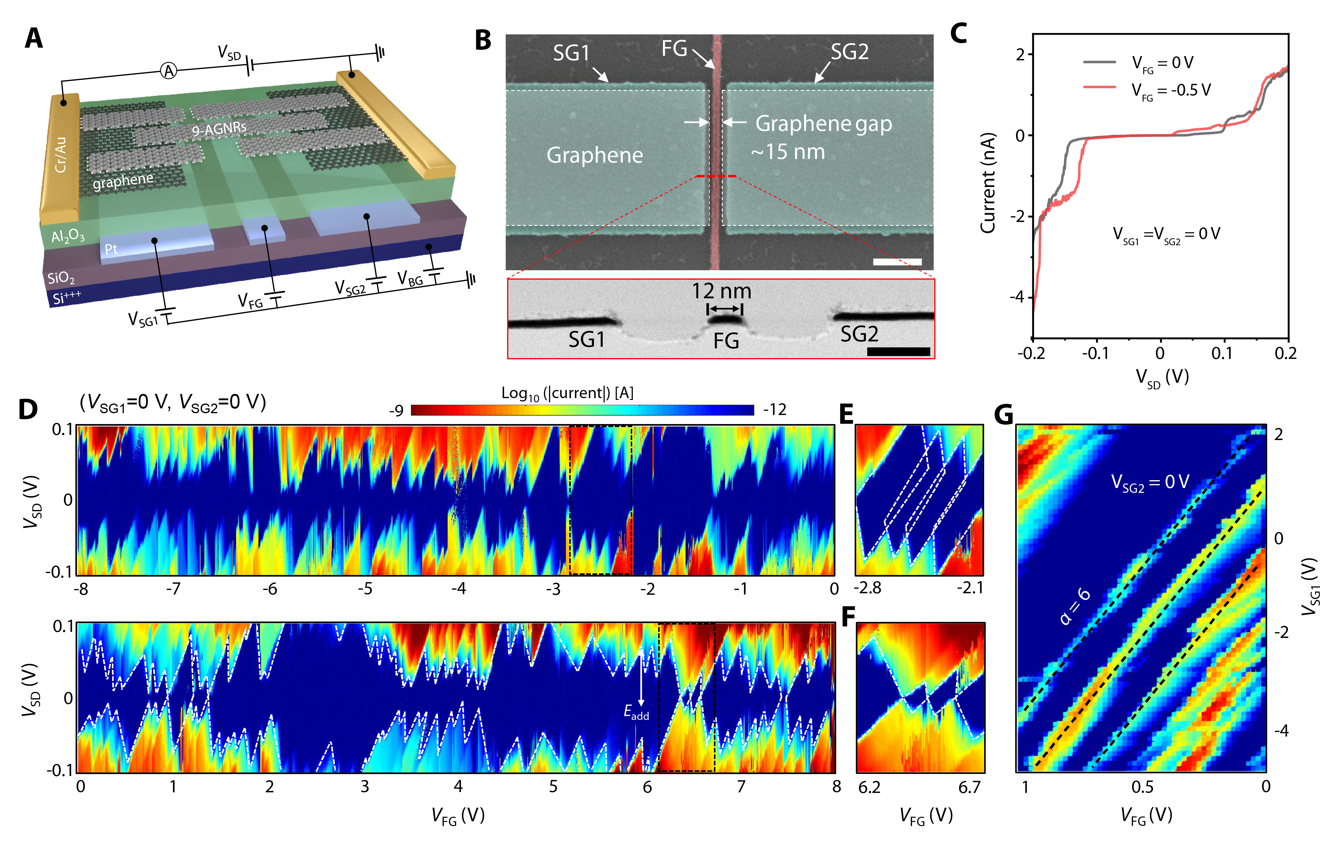
The starting point of the sample fabrication is a highly-doped silicon (Si) carrier chip with a 285 nm thick silicon dioxide (SiO2), such that the Si substrate acts as a global back gate (BG). The finger gates are patterned on top as follows. First an 8 nm platinum (Pt) film is deposited using electron-beam evaporation. Then, a negative resist hydrogen silesquioxane (HSQ) is spin-coated as a resist to define the etch mask. This resist turns into SiO2-like after EBL exposure and development, leading to a highly-resistive etch mask. A subsequent Ar+-ion milling step transfers the etch mask feature to the metal film, separating the finger from the side gates. This process leads to very sharp features as it is not limited by grain sizes or other edges effects which are common when using electron-beam evaporation with a lift-off process. Our approach results in a finger gate with a length of 10-15 nm and a width of 500 nm. The nanometer-scale dimension of the FG () allows for creating an ultra-short effective channel length while minimizing parasitic gate to source-drain capacitance. The 9-AGNRs junction is electrically isolated from the metal gates using a 30 nm thick aluminum oxide (Al2O3). The graphene electrodes are separated by a nanogap formed with high-resolution patterning by using EBL, as reported elsewhere.27 Here, the electrode separation is set to be 15 nm, large enough to eliminate direct tunneling contributions between the electrodes, but smaller than the average length of the 9-AGNRs. 37 In Section 2 of the Supporting Information, a more detailed description of the fabrication process is given.A scanning electron micrograph (SEM) of the final device before GNR transfer is presented in Fig. 1b, alongside a transmission electron micrograph (TEM). The image shows that the FG length is 12 nm, and the separation between the gates 30 nm.
1.2 Quantum dot formation at low temperature
Prior to the deposition of the GNRs, the nanogaps were electrically characterized to ensure a clear separation between the electrodes. Devices with currents 10 pA at V = 4 V were excluded from further characterization (See Section 3.1 of the Supporting Information). Uniaxially aligned medium-density 9-AGNRs were synthesized on an Au(788) single crystal under ultrahigh vacuum conditions (See Materials and Methods).38 A representative scanning tunneling micrograph is presented in Section 4 of the Supporting Information. The average GNR density is about 2 GNRs per terrace (3-4 nm in width), with an average length between 40-45 nm.37 The 9-AGNRs were then transferred to the multi-gate device substrate with the predefined and characterized graphene electrodes using a PMMA-based electrochemical delamination process.38, 39, 40 In order to improve the device performance, a thermal annealing step was performed.27 After this thermal annealing step the integrity of the 9-AGNRs and their alignment with respect to the source-drain axis was confirmed using polarization-dependent Raman spectroscopy (See Section 4 of the Supporting Information).
To evaluate the electrical properties of the 9-AGNRs after device integration, we recorded stability diagrams (current-voltage characteristics (IV) for varying FG voltage V at T = 9 K). Two IVs are presented in Figure 1c for different finger gate voltages, both exhibiting blocked current at low bias voltage and multiple steps in current for increase bias voltages. These steps are typical for quantum dot behavior41.
Figure 1d shows a stability diagram recorded with the voltages on SG1, SG2 and BG all set to 0 V. The plot shows irregular and aperiodic Coulomb diamonds (CD) over a FG voltage range of 16 V (-8 V to 8 V), with addition energies () varying between 20 meV and 150 meV. Given the nanometer size of the GNRs, and in particular their extremely narrow width of 1 nm, we attribute these Coulomb diamonds to the formation of quantum dots in the GNRs with a discrete level structure18, 42.
The lever arm for the FG, = /, is determined to be in the range of 220-340 mV/V from the Coulomb diamonds, indicating a very strong gate coupling of the finger gate to the 9-AGNRs. For a large portion of the FG range, no crossing of the corresponding energy level with the Fermi energy of the electrodes is observed, i.e., no resonance is visible at zero bias. This behavior is highlighted in Fig. 1e for a gate range from -2.8 V to -2.1 V and is attributed to transport through two weakly-coupled QDs in series. Here, the serial QDs correspond most likely to different GNRs, but possibly also to the formation of localized states within a single GNR due to the presence of bite defects.43 In other gate regimes, for example in Fig. 1f, the Coulomb diamonds are closing, indicating that in this gate range a single level of a QD is dominating the transport. Although not very likely, this feature could also be associated with multiple quantum dots in series with very similar energies. We also observe multiple overlapping diamonds with different addition energies, suggesting that charge transport occurs through two or more parallel QDs, presumably individual GNRs, with different energy spectra.44 These differences could be caused by different GNR length and local environments. The stability diagrams of devices 2-4 show similar features as Device 1 (see Supporting Information Section 3.2).
To investigate the additional control offered by the side gates, we recorded a map of the current as a function of V and V for a fixed source-drain voltage V = 100 mV, as shown in Fig. 1g. The plot displays multiple regions of high current that shift with the gate voltages and appear as lines. Three such lines of enhanced current are marked with black dashed lines. From the slopes we extract the relative gate coupling between FG and SG1 and find 5.98, revealing that the FG couples more strongly to the GNR than the SGs. In this gate range, we do not observe any distinct signature of a double quantum dot system, with access to multiple charge states. We attribute this to the presence of multiple GNRs in the channel. In section 1 of the Supporting Information, we perform finite-element calculations to model the electrostatic potential in the junction area as a function of the voltages applied on the side gates and finger gate. Here, a relative gate coupling of around 10 is found, close to the experimentally observed value of 6. The difference between experiment and theory may be caused by local variations in the sample geometry, such as the gate and/or the gate oxide, or a slight misalignment of the graphene gap with respect to the finger gate.
1.3 Effect of side gates
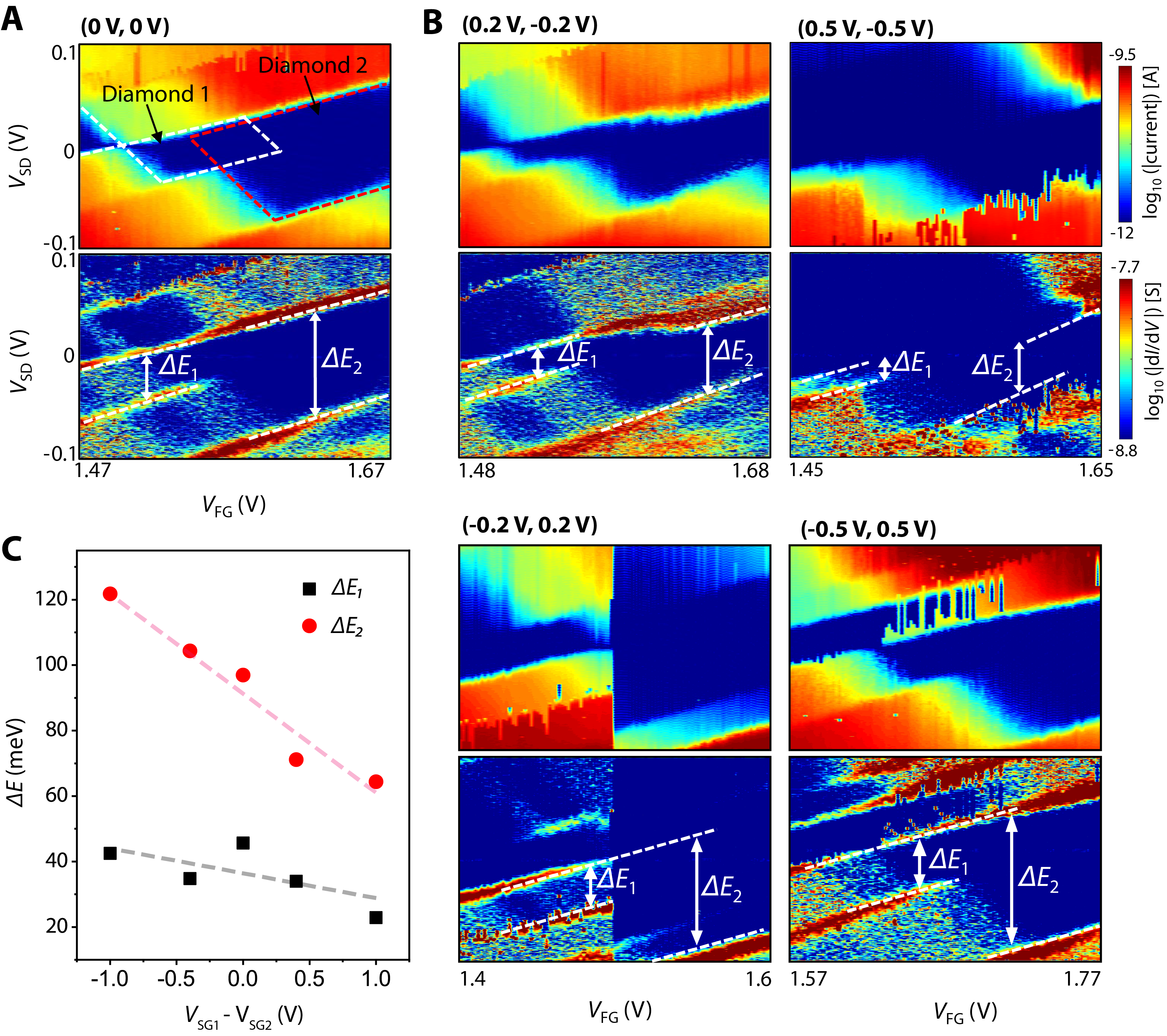
In Fig. 2, we further characterize the effect of the side gates, and in particular on the electronic structure of the QDs formed in the device. We measure the current maps as a function of the finger gate voltage V for different side gate voltages V and V (later indicated in brackets). The top panel of Fig. 2a presents the (0 V, 0 V) case, focusing on the finger gate voltage range around +1.6 V, where two diamonds of different sizes overlap, indicating two QDs with different physical size are weakly coupled and contacted in series. The lower panel shows the dI/dV plots, from which energy differences between the energy levels for different dots are identified, as indicated by and . We note that these energies do not correspond to the addition energies of the two QDs. To extract the relative gating of the two QDs by the side gates, we perform the same stability diagram but now for different values of the side gates. To maximize the asymmetry of the electric field introduced in the nanojunctions, we apply voltages of opposite polarities on the two side gates. In Fig. 2b, we plot the current and dI/dV maps for four different side gate combinations. The figures show that the side gates significantly alter the shape and size of the two diamonds. Fig. 2c shows the energy difference and as a function of the voltage difference between V and V. The plots show that is strongly modulated by the asymmetric gate field, with a shift of about 30 meV / 1 V. , on the other hand, has a shift of about 10 meV / 1 V. This observation suggests that the asymmetric field introduced by the side gates leads to differential gating of one QD versus the other. This also implied that one of the QD is closer to one of the side gates.
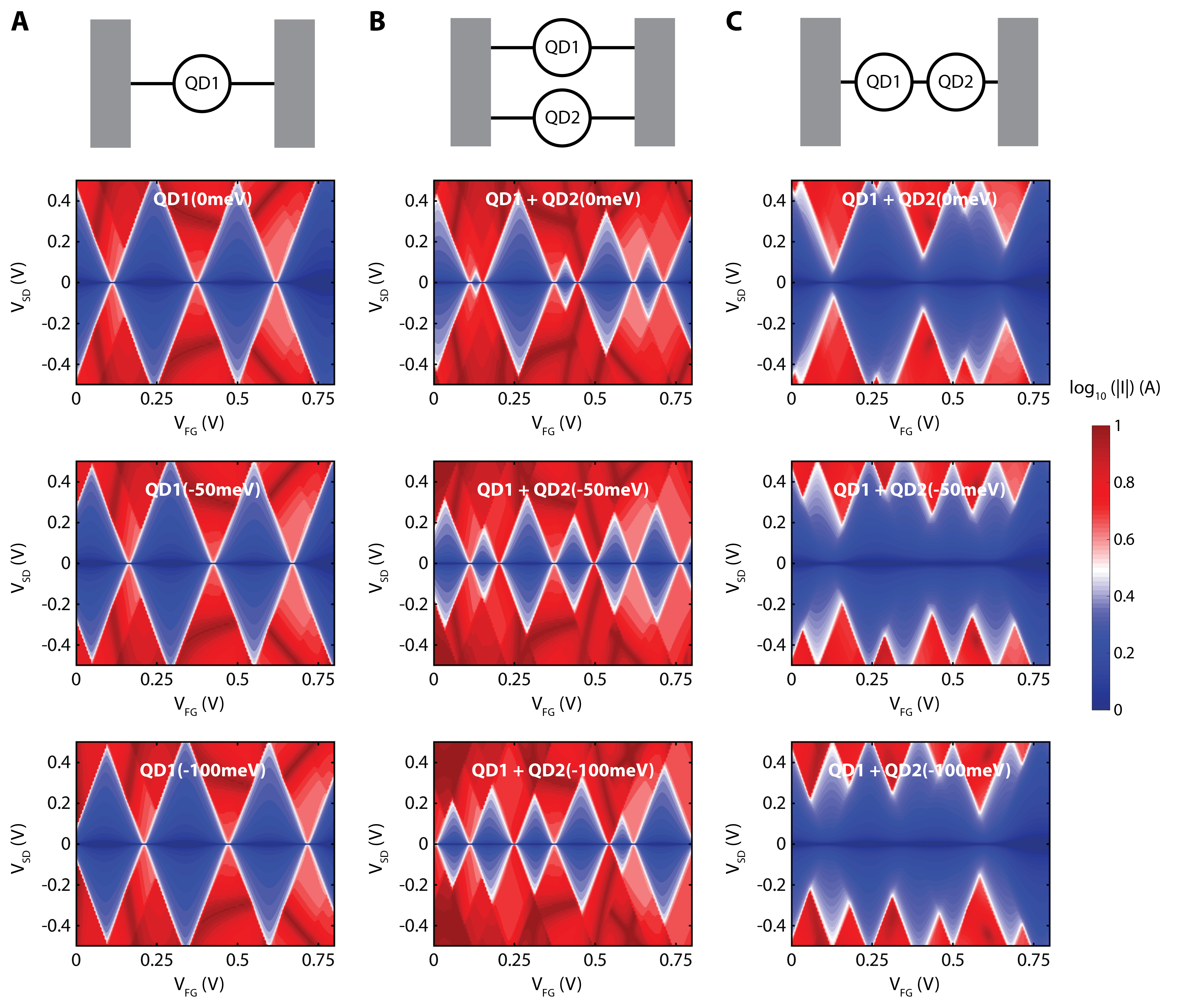
To rationalize the experimental observations shown in Fig. 1 and Fig. 2, we performed quantum transport calculations45 through single and multiple dots in series and parallel using a simple tight-binding model (see details in the Materials and Methods, and in supporting information Section 5). The two QDs have each a different level structure with addition energies that are nonetheless comparable in size. We assume that the main bias potential drop happens at the contact point to electrodes and remains constant over the QDs. This is a good approximation because the coupling to electrodes is weak. In Fig. 3a, we show the single QD case, with three current vs. FG voltage maps (stability diagrams). The top current map shows the current modulation by only the FG voltage. In the middle and bottom current map, to mimic the electrostatic potential change induced by the two side gates, the overall energy spectrum of the QD is shifted by -50 and -100 meV, respectively. We note that the effective potential experienced by the QD as a result of the two side gates will depend on its position in the nanojunction and the applied side gate voltages. Figure 3b and Fig. 3c present the same plots, but for two QDs in parallel and in series, respectively. Here, the asymmetry is modelled by moving the energy levels of QD2 with to those of QD1. As the two QDs have a comparable level structure, the stability diagrams for transport in parallel and series appear to be fairly similar. Nevertheless, current in parallel is about twice as large and an additional crossing point appears very close to those already present for the single QD case. For the series case, the current is twice as small and some crossing points are fading out. The situation becomes very different when QD2 is being shifted. In the parallel case, additional diamonds appear and grow in size, while the existing ones are being reduced. In series, the crossing points fade out even more until the diamonds do not close anymore. These plots indicate that the energy shift of one of the QDs in series with respect to the other, as induced by an asymmetric gate field, can drastically alter the electronic properties of the nano-junctions.
 |
2 Conclusion and Discussion
We developed a multi-gate FET geometry to contact uniaxially aligned 9-AGNRs that are contacted by graphene electrodes. At low temperatures, Coulomb blockade and single-electron tunneling is observed, with a very strong gate coupling of the finger gate to the 9-AGNRs, up to 340 meV/V. In addition, we demonstrate the additional tunability offered by the two side gates that are present in our device architecture and allow for differential electrostatic tuning of the multiple QDs present in the junction.
The observed addition energies of 0.065 eV are in discrepancy with the DFT-calculated bandgap of 0.73 eV 18 as well as the measured bandgap using scanning tunneling spectroscopy (STS) of 1.40 eV46. However, in our measurements, many QDs are presumably bridging the two electrodes in parallel and series, making the task of extracting the exact addition energy challenging. In particular, as observed in Fig. 3b, the effective diamond sizes is reduced when multiple QDs are connected in parallel, leading to an underestimation of the addition energies of the individual QDs. The multiple GNRs in the nanojunction also make it such that the QDs in series do not form an ideal double-dot system, in which each gate tunes primarily the levels of the closest QD. This aspect is further highlighted by the fact that different quantum dots couple differently to the different gates, illustrating the challenges in the exact positioning of the nanoscale gates, nanogaps, and GNRs with respect to each other.
Further efforts in reducing the electrode size for contacting fewer GNRs would be valuable for characterizing the physical properties of a single GNR integrated into devices, possibly by downscaling the width of the graphene electrode, or by using electrode materials that are naturally close to the atomic level, for example, carbon nanotubes47. Along similar lines, our approach might be further pushed towards an ultimately-narrow gate by using a carbon nanotube48 or even the edge of a graphene sheet30 as gate electrodes, as demonstrated for MoS2-FETs. Finally, several charge jumps are observed in our measured stability diagrams, highlighting the fact that the effect of the substrate needs to be better controlled, for example, via encapsulation in hBN.
Overall, the differential gating of the QDs using multiple gates is a major step forward in the exploration of the transport characteristics of GNRs and their exploitation in future electronic device architectures.49 With further development, more advanced electronic quantum devices may be envisioned in which several gates are required to achieve the required control over the electrostatic landscape. In particular, the controlled formation of double quantum dot systems based on GNRs offers exciting prospects for the realization of GNR-based quantum technologies such as spin qubits that possess operation conditions above dilution refrigerators temperatures.
Materials and Methods
Fabrication of multi-gate device substrates
A detailed description is given in Supporting Information Section 2. In brief, a highly -doped silicon (500 m) with a thermally grown silicon dioxide layer (285 nm) is used as a base substrate. A titanium/platinum thin film (1 nm/8 nm) is evaporated on top and a negative resist hydrogen silesquioxane (HSQ) is spin-coated as a resist to define the etch mask. This resist turns into SiO2-like film after EBL exposure and development, leading to a highly-resistive etch mask. A subsequent Ar+-ion milling step transfers the etch mask feature to the metal film, separating the finger from the side gates.
Graphene growth, transfer, and nanogap formation
Polycrystalline graphene is synthesized via chemical vapor deposition (CVD), transferred, and pre-patterned as reported elsewhere.27 After a first prepatterning of the graphene, a 60 nm thick CSAR resist (AR-P 6200.04, Allresist GmbH) is spin-coated. Following the second electron beam exposure, the resist is developed using a suitable developer (AR 600-546, Allresist GmbH) at room temperature for 1 min followed by an IPA rinse. Reactive ion etching, RIE (15 sccm Ar, 30 sccm O, 25 W, 18 mTorr) for 6-8 s was used to cut the graphene within the CSAR gap. After RIE, the etching mask is removed by immersing in 1-Methyl-2-pyrrolidinone (NMP) (Sigma Aldrich) at room temperature for 10 min followed by 60 min at 80 ∘C, cooled down for 30 min, rinsed with IPA, and blown dry with N2. This approach yield clean and well-separated graphene electrodes (15 nm nanogaps).
On-surface synthesis of aligned 9-AGNRs and transfer to device substrate
9-AGNRs were synthesized from 3’,6’-diiodo-1,1’:2’,1”-terphenyl (DITP). 37 Using a Au(788) single crystal (MaTeK, Germany) as growth substrate results in uniaxially aligned 9-AGNRs (GNRs grown along the narrow Au(111) terraces).38 The Au(788) surface is cleaned in ultrahigh vacuum by two sputtering/annealing cycles: 1 kV Ar+ for 10 min followed by annealing at 420 ∘C for 10 min. Next, the precursor monomer DITP is sublimed onto the Au(788) surface from a quartz crucible heated to 70 ∘C, with the substrate held at room temperature. After deposition of about 60%-70% of one monolayer DITP, the substrate is heated (0.5 K/s) to 200 ∘C with a 10 min holding time to activate the polymerization reaction, followed by annealing at 400 ∘C (0.5 K/s with a 10 min holding time) to form the GNRs via cyclodehydrogenation. The average GNR length is between 40 and 45 nm.37 9-AGNRs are transferred from their growth substrate to the silicon-based substrates with predefined graphene electrodes by an electrochemical delamination method using PMMA as described previously.38, 39, 40 As the transfer of the 9-AGNRs onto the substrate exposes the graphene electrodes to water, the samples were heated to 200 ∘C for 120 minutes at 10-6 mbar to remove water residues at the graphene/GNR interface and improve the device performance.27
Electronic measurements
All electronic measurements were performed under vacuum conditions (10-6 mbar). The devices were measured in a commercially available probe station (Lake Shore Cryogenics, Model CRX-6.5K) at various temperatures (9 K - 350 K). A data acquisition board (ADwin-Gold II, Jäger Computergesteuerte Messtechnik GmbH) is employed to apply the bias and gate voltages and read the voltage output of the I–V converter (DDPCA-300, FEMTO Messtechnik GmbH).
Theoretical methods
To model transport through the junctions formed by 9-AGNRs connected to two graphene electrodes, we construct a tight-binding (TB) model of a chain of atoms with one orbital per atom to represent graphene ribbons connected to a 1D chain of atoms as shown in Fig. 11 of the SI. To construct the TB Hamiltonian, all on-site energies are set to zero in the electrodes. The on-site energies for one of the chains representing a ribbon (QD1) are set to zero whereas for the other one (QD2) varies to represent an offset between the energy levels of two ribbons. We assume that the main bias voltage drop happens at the connection point to the electrodes and that the bias potential profile is constant over all sites in the scattering region (see Fig. 11 of the SI). The gate voltage is tuned between -2V and 2V. We employ scattering theory and calculate transmission coefficients for each chain (T1 and T2) representing each ribbon and then use expression 1/T=1/T1+1/T2 to calculate the total transmission (T). To take the effect of addition energy (Coulomb energy) into account, we follow the procedure as in ref 45 and apply constant addition energy U=0.4eV to both QDs. The current then is calculated from the total transmission (T) using the Landauer formula 45 .
Acknowledgements
J.Z. acknowledges funding from the EMPAPOSTDOCS-II program which is financed by the European Union Horizon 2020 research and innovation program under the Marie Skłodowska-Curie grant agreement number 754364. O.B. and M.C. acknowledge funding by the EC H2020 FET Open project no. 767187 (QuIET). M.L.P. acknowledges funding from the Swiss National Science Foundation under Spark grant no. 196795 and the Eccellenza Professorial Fellowship no. PCEFP2_203663, as well as support by the Swiss State Secretariat for Education, Research and Innovation (SERI) under contract number MB22.00076. M.C. acknowledges funding from the Swiss National Science Foundation under the Sinergia grant no. 189924 (Hydronics). H.S. acknowledges the UKRI for Future Leaders Fellowship number MR/S015329/2. S.S. acknowledges the Leverhulme Trust for Early Career Fellowship no. ECF-2018-375. R.F. acknowledges funding by the Swiss National Science Foundation under grant no. 182015. G.B.B., P.F. and R.F. acknowledge the European Union Horizon 2020 research and innovation program under grant agreement no. 881603 (GrapheneFlagship Core 3) and the Office of Naval Research BRC Program under the grant N00014-18-1-2708. G.B.B., R.D., P.F. and R.F. also greatly appreciate the financial support from the Werner Siemens Foundation (CarboQuant). The authors acknowledge support from the Multiphysics Hub @ Empa for the COMSOL Multiphyics calculations, as well as the Cleanroom Operations Team of the Binnig and Rohrer Nanotechnology Center (BRNC) for their help and support.
Author contributions
Conceptualization: M.C., J.Z., O.B., M.L.P, J.O. Methodology: J.Z., O.B., J.O., S.S., H.S., M.L.P, I.S. Investigation: J.Z., O.B., M.L.P., J.O., M.S., A.O., H.S., S.S., A.H.S.D. Resources: R. Fu., G.B.B., R.D., K.M. Visualization: M.L.P., J.Z., O.B. Supervision: P.R., R.F., H.S., M.L.P., M.C. Writing—original draft: O.B., J.Z., S.S., H.S., M.L.P., M.C. Writing—review & editing: J.Z., O.B., M.L.P., M.C., H.S., S.S., A.H.S.D., J.O., I.S., M.S., A.O., G.B.B., R.D., K.M., R.F., P.R.
Competing interests
The authors declare that they have no competing interests.
Data availability
The datasets generated during and/or analysed during the current study are available from the authors on reasonable request.
References
- Gunlycke et al. 2007 Gunlycke, D.; Lawler, H.; White, C. Room-temperature ballistic transport in narrow graphene strips. Physical Review B 2007, 75, 085418
- Stampfer et al. 2009 Stampfer, C.; Güttinger, J.; Hellmüller, S.; Molitor, F.; Ensslin, K.; Ihn, T. Energy gaps in etched graphene nanoribbons. Physical review letters 2009, 102, 056403
- Wang et al. 2022 Wang, X.; Song, S.; Wang, H.; Guo, T.; Xue, Y.; Wang, R.; Wang, H.; Chen, L.; Jiang, C.; Chen, C.; Shi, Z.; Wu, T.; Song, W.; Zhang, S.; Watanabe, K.; Taniguchi, T.; Song, Z.; Xie, X. Minimizing the Programming Power of Phase Change Memory by Using Graphene Nanoribbon Edge-Contact. Advanced Science 2022, 9, 2202222
- Cai et al. 2010 Cai, J.; Ruffieux, P.; Jaafar, R.; Bieri, M.; Braun, T.; Blankenburg, S.; Muoth, M.; Seitsonen, A. P.; Saleh, M.; Feng, X.; Müllen, K.; Fasel, R. Atomically Precise Bottom-up Fabrication of Graphene Nanoribbons. Nature 2010, 466, 470–473
- Liu et al. 2015 Liu, J.; Li, B.-W.; Tan, Y.-Z.; Giannakopoulos, A.; Sanchez-Sanchez, C.; Beljonne, D.; Ruffieux, P.; Fasel, R.; Feng, X.; Muellen, K. Toward Cove-edged Low Band Gap Graphene Nanoribbons. Journal of the American Chemical Society 2015, 137, 6097–6103
- Cai et al. 2014 Cai, J.; Pignedoli, C. A.; Talirz, L.; Ruffieux, P.; Soede, H.; Liang, L.; Meunier, V.; Berger, R.; Li, R.; Feng, X.; Muellen, K.; Fasel, R. Graphene Nanoribbon Heterojunctions. Nature Nanotechnology 2014, 9, 896–900
- Ruffieux et al. 2016 Ruffieux, P.; Wang, S.; Yang, B.; Sanchez-Sanchez, C.; Liu, J.; Dienel, T.; Talirz, L.; Shinde, P.; Pignedoli, C. A.; Passerone, D.; Dumslaff, T.; Feng, X.; Muellen, K.; Fasel, R. On-surface Synthesis of Graphene Nanoribbons with Zigzag Edge Topology. Nature 2016, 531, 489
- Groning et al. 2018 Groning, O.; Wang, S.; Yao, X.; Pignedoli, C. A.; Barin, G. B.; Daniels, C.; Cupo, A.; Meunier, V.; Feng, X.; Narita, A.; Muellen, K.; Ruffieux, P.; Fasel, R. Engineering of Robust Topological Quantum Phases in Graphene Nanoribbons. Nature 2018, 560, 209
- Rizzo et al. 2018 Rizzo, D. J.; Veber, G.; Cao, T.; Bronner, C.; Chen, T.; Zhao, F.; Rodriguez, H.; Louie, S. G.; Crommie, M. F.; Fischer, F. R. Topological Band Engineering of Graphene Nanoribbons. Nature 2018, 560, 204–208
- Sun et al. 2020 Sun, Q.; Gröning, O.; Overbeck, J.; Braun, O.; Perrin, M. L.; Borin Barin, G.; El Abbassi, M.; Eimre, K.; Ditler, E.; Daniels, C.; Meunier, V.; Pignedoli, C. A.; Calame, M.; Fasel, R.; Ruffieux, P. Massive Dirac Fermion Behavior in a Low Bandgap Graphene Nanoribbon near a Topological Phase Boundary. Advanced Materials 2020, 32, 1906054
- Yamaguchi et al. 2020 Yamaguchi, J.; Hayashi, H.; Jippo, H.; Shiotari, A.; Ohtomo, M.; Sakakura, M.; Hieda, N.; Aratani, N.; Ohfuchi, M.; Sugimoto, Y.; Yamada, H.; Sato, S. Small Bandgap in Atomically Precise 17-atom-wide Armchair-edged Graphene Nanoribbons. Communications Materials 2020, 1, 36
- Chen et al. 2020 Chen, Z.; Narita, A.; Müllen, K. Graphene Nanoribbons: On-surface Synthesis and Integration into Electronic Devices. Advanced Materials 2020, 32, 2001893
- Li et al. 2020 Li, Y. L.; Zee, C.-T.; Lin, J. B.; Basile, V. M.; Muni, M.; Flores, M. D.; Munárriz, J.; Kaner, R. B.; Alexandrova, A. N.; Houk, K. N.; Tolbert, S. H.; Rubin, Y. Fjord-edge Graphene Nanoribbons with Site-specific Nitrogen Substitution. Journal of the American Chemical Society 2020, 142, 18093–18102
- Pawlak et al. 2020 Pawlak, R.; Liu, X.; Ninova, S.; D’Astolfo, P.; Drechsel, C.; Sangtarash, S.; Häner, R.; Decurtins, S.; Sadeghi, H.; Lambert, C. J.; Aschauer, U.; Liu, S.-X.; Meyer, E. Bottom-up Synthesis of Nitrogen-doped Porous Graphene Nanoribbons. Journal of the American Chemical Society 2020, 142, 12568–12573
- Sun et al. 2020 Sun, Q.; Yao, X.; Gröning, O.; Eimre, K.; Pignedoli, C. A.; Müllen, K.; Narita, A.; Fasel, R.; Ruffieux, P. Coupled Spin States in Armchair Graphene Nanoribbons with Asymmetric Zigzag Edge Extensions. Nano Letters 2020, 20, 6429–6436
- Cirera et al. 2020 Cirera, B.; Sánchez-Grande, A.; de la Torre, B.; Santos, J.; Edalatmanesh, S.; Rodríguez-Sánchez, E.; Lauwaet, K.; Mallada, B.; Zbořil, R.; Miranda, R.; Gröning, O.; Jelínek, P.; Martín, N.; Ecija, D. Tailoring Topological Order and -conjugation to Engineer Quasi-metallic Polymers. Nature Nanotechnology 2020, 15, 437–443
- Yang et al. 2022 Yang, L.; Ma, J.; Zheng, W.; Osella, S.; Droste, J.; Komber, H.; Liu, K.; Böckmann, S.; Beljonne, D.; Hansen, M. R.; Bonn, M.; Wang, H. I.; Liu, J.; Feng, X. Solution Synthesis and Characterization of a Long and Curved Graphene Nanoribbon with Hybrid Cove–Armchair–Gulf Edge Structures. Advanced Science 2022, 9, 2200708
- Son et al. 2006 Son, Y.-W.; Cohen, M. L.; Louie, S. G. Energy Gaps in Graphene Nanoribbons. Physical Review Letters 2006, 97, 216803
- Kimouche et al. 2015 Kimouche, A.; Ervasti, M. M.; Drost, R.; Halonen, S.; Harju, A.; Joensuu, P. M.; Sainio, J.; Liljeroth, P. Ultra-narrow Metallic Armchair Graphene Nanoribbons. Nature Communications 2015, 6, 10177
- Wang et al. 2016 Wang, S.; Talirz, L.; Pignedoli, C. A.; Feng, X.; Müllen, K.; Fasel, R.; Ruffieux, P. Giant edge state splitting at atomically precise graphene zigzag edges. Nature communications 2016, 7, 1–6
- Cao et al. 2017 Cao, T.; Zhao, F.; Louie, S. G. Topological Phases in Graphene Nanoribbons: Junction States, Spin Centers, and Quantum Spin Chains. Physical Review Letters 2017, 119, 076401
- Llinas et al. 2017 Llinas, J. P.; Fairbrother, A.; Borin Barin, G.; Shi, W.; Lee, K.; Wu, S.; Yong Choi, B.; Braganza, R.; Lear, J.; Kau, N.; Choi, W.; Chen, C.; Pedramrazi, Z.; Dumslaff, T.; Narita, A.; Feng, X.; Müllen, K.; Fischer, F.; Zettl, A.; Ruffieux, P. et al. Short-channel Field-effect Transistors with 9-atom and 13-atom Wide Graphene Nanoribbons. Nature Communications 2017, 8, 633
- Martini et al. 2019 Martini, L.; Chen, Z.; Mishra, N.; Barin, G. B.; Fantuzzi, P.; Ruffieux, P.; Fasel, R.; Feng, X.; Narita, A.; Coletti, C.; Müllen, K.; Candini, A. Structure-dependent Electrical Properties of Graphene Nanoribbon Devices with Graphene Electrodes. Carbon 2019, 146, 36–43
- Passi et al. 2018 Passi, V.; Gahoi, A.; Senkovskiy, B. V.; Haberer, D.; Fischer, F. R.; Grüneis, A.; Lemme, M. C. Field-effect Transistors Based on Networks of Highly Aligned, Chemically Synthesized N = 7 Armchair Graphene Nanoribbons. ACS Applied Materials and Interfaces 2018, 10, 9900–9903
- El Abbassi et al. 2020 El Abbassi, M.; Perrin, M. L.; Barin, G. B.; Sangtarash, S.; Overbeck, J.; Braun, O.; Lambert, C. J.; Sun, Q.; Prechtl, T.; Narita, A.; Müllen, K.; Ruffieux, P.; Sadeghi, H.; Fasel, R.; Calame, M. Controlled Quantum Dot Formation in Atomically Engineered Graphene Nanoribbon Field-effect Transistors. ACS Nano 2020, 14, 5754–5762
- Richter et al. 2020 Richter, N.; Chen, Z.; Tries, A.; Prechtl, T.; Narita, A.; Müllen, K.; Asadi, K.; Bonn, M.; Kläui, M. Charge Transport Mechanism in Networks of Armchair Graphene Nanoribbons. Scientific Reports 2020, 10, 1–8
- Braun et al. 2021 Braun, O.; Overbeck, J.; Abbassi, M. E.; Käser, S.; Furrer, R.; Olziersky, A.; Flasby, A.; Barin, G. B.; Darawish, R.; Müllen, K., et al. Optimized Graphene Electrodes for contacting Graphene Nanoribbons. Carbon 2021, 184, 331–339
- Senkovskiy et al. 2021 Senkovskiy, B. V.; Nenashev, A. V.; Alavi, S. K.; Falke, Y.; Hell, M.; Bampoulis, P.; Rybkovskiy, D. V.; Usachov, D. Y.; Fedorov, A. V.; Chernov, A. I., et al. Tunneling current modulation in atomically precise graphene nanoribbon heterojunctions. Nature communications 2021, 12, 1–11
- Saraswat et al. 2021 Saraswat, V.; Jacobberger, R. M.; Arnold, M. S. Materials Science Challenges to Graphene Nanoribbon Electronics. ACS nano 2021, 15, 3674–3708
- Wu et al. 2022 Wu, F.; Tian, H.; Shen, Y.; Hou, Z.; Ren, J.; Gou, G.; Sun, Y.; Yang, Y.; Ren, T.-L. Vertical MoS2 transistors with sub-1-nm gate lengths. Nature 2022, 603, 259–264
- Jiang et al. 2020 Jiang, J.; Doan, M.-H.; Sun, L.; Kim, H.; Yu, H.; Joo, M.-K.; Park, S. H.; Yang, H.; Duong, D. L.; Lee, Y. H. Ultrashort Vertical-Channel van der Waals Semiconductor Transistors. Advanced Science 2020, 7, 1902964
- El Abbassi et al. 2019 El Abbassi, M.; Sangtarash, S.; Liu, X.; Perrin, M. L.; Braun, O.; Lambert, C.; van der Zant, H. S. J.; Yitzchaik, S.; Decurtins, S.; Liu, S.-X.; Sadeghi, H.; Calame, M. Robust Graphene-based Molecular Devices. Nature Nanotechnology 2019, 14, 957–961
- Radisavljevic et al. 2011 Radisavljevic, B.; Radenovic, A.; Brivio, J.; Giacometti, V.; Kis, A. Single-layer MoS 2 transistors. Nature nanotechnology 2011, 6, 147–150
- Marega et al. 2020 Marega, G. M.; Zhao, Y.; Avsar, A.; Wang, Z.; Tripathi, M.; Radenovic, A.; Kis, A. Logic-in-memory based on an atomically thin semiconductor. Nature 2020, 587, 72–77
- Liu et al. 2021 Liu, L.; Kong, L.; Li, Q.; He, C.; Ren, L.; Tao, Q.; Yang, X.; Lin, J.; Zhao, B.; Li, Z., et al. Transferred van der Waals metal electrodes for sub-1-nm MoS2 vertical transistors. Nature Electronics 2021, 4, 342–347
- Wu et al. 2007 Wu, Y.; Lin, H.; Ye, P.; Wilk, G. Current transport and maximum dielectric strength of atomic-layer-deposited ultrathin Al 2 O 3 on GaAs. Applied physics letters 2007, 90, 072105
- Di Giovannantonio et al. 2018 Di Giovannantonio, M.; Deniz, O.; Urgel, J. I.; Widmer, R.; Dienel, T.; Stolz, S.; Sánchez-Sánchez, C.; Muntwiler, M.; Dumslaff, T.; Berger, R.; Narita, A.; Feng, X.; Müllen, K.; Ruffieux, P.; Fasel, R. On-surface Growth Dynamics of Graphene Nanoribbons: The Role of Halogen Functionalization. ACS Nano 2018, 12, 74–81
- Overbeck et al. 2019 Overbeck, J.; Borin Barin, G.; Daniels, C.; Perrin, M. L.; Liang, L.; Braun, O.; Darawish, R.; Burkhardt, B.; Dumslaff, T.; Wang, X. Y.; Narita, A.; Müllen, K.; Meunier, V.; Fasel, R.; Calame, M.; Ruffieux, P. Optimized Substrates and Measurement Approaches for Raman Spectroscopy of Graphene Nanoribbons. Physica Status Solidi (b) Basic Research 2019, 256, 1900343
- Senkovskiy et al. 2017 Senkovskiy, B.; Pfeiffer, M.; Alavi, S.; Bliesener, A.; Zhu, J.; Michel, S.; Fedorov, A.; German, R.; Hertel, D.; Haberer, D.; Petaccia, L.; Fischer, F.; Meerholz, K.; van Loosdrecht, P.; Lindfors, K.; Grüneis, A. Making graphene nanoribbons photoluminescent. Nano letters 2017, 17, 4029–4037
- Overbeck et al. 2019 Overbeck, J.; Barin, G. B.; Daniels, C.; Perrin, M. L.; Braun, O.; Sun, Q.; Darawish, R.; De Luca, M.; Wang, X. Y.; Dumslaff, T.; Narita, A.; Müllen, K.; Ruffieux, P.; Meunier, V.; Fasel, R.; Calame, M. A Universal Length-dependent Vibrational Mode in Graphene Nanoribbons. ACS Nano 2019, 13, 13083–13091
- Kouwenhoven et al. 1997 Kouwenhoven, L. P.; Marcus, C. M.; McEuen, P. L.; Tarucha, S.; Westervelt, R. M.; Wingreen, N. S. In Mesoscopic Electron Transport; Sohn, L. L., Kouwenhoven, L. P., Schön, G., Eds.; Springer Netherlands: Dordrecht, 1997; pp 105–214
- Merino-Díez et al. 2017 Merino-Díez, N.; Garcia-Lekue, A.; Carbonell-Sanromà, E.; Li, J.; Corso, M.; Colazzo, L.; Sedona, F.; Sánchez-Portal, D.; Pascual, J. I.; de Oteyza, D. G. Width-dependent Band Gap in Armchair Graphene Nanoribbons Reveals Fermi Level Pinning on Au(111). ACS Nano 2017, 11, 11661–11668, PMID: 29049879
- Pizzochero et al. 2021 Pizzochero, M.; Čerņevičs, K.; Barin, G. B.; Wang, S.; Ruffieux, P.; Fasel, R.; Yazyev, O. V. Quantum electronic transport across ‘bite’ defects in graphene nanoribbons. 2D Materials 2021, 8, 035025
- 44 Ionica, I.; Montès, L.; Zimmermann, J.; Saminadayar, L.; Bouchiat, V. Influence of the Geometry on the Coulomb Blockade in Silicon Nanostructures.
- Sadeghi 2018 Sadeghi, H. Theory of Electron, Phonon and Spin Transport in Nanoscale Quantum Devices. Nanotechnology 2018, 29, 373001
- Talirz et al. 2017 Talirz, L.; Sode, H.; Dumslaff, T.; Wang, S.; Sanchez-Valencia, J. R.; Liu, J.; Shinde, P.; Pignedoli, C. A.; Liang, L.; Meunier, V.; Plumb, N. C.; Shi, M.; Feng, X.; Narita, A.; Muellen, K.; Fasel, R.; Ruffieux, P. On-surface Synthesis and Characterization of 9-atom Wide Armchair Graphene Nanoribbons. ACS Nano 2017, 11, 1380–1388
- Zhang et al. 2022 Zhang, J.; Calame, M.; Perrin, M. L. Contacting atomically precise graphene nanoribbons for next-generation quantum electronics. Matter 2022, 5, 2497–2499
- Desai et al. 2016 Desai, S. B.; Madhvapathy, S. R.; Sachid, A. B.; Llinas, J. P.; Wang, Q.; Ahn, G. H.; Pitner, G.; Kim, M. J.; Bokor, J.; Hu, C.; Wong, H.-S. P.; Javey, A. MoS2 transistors with 1-nanometer gate lengths. Science 2016, 354, 99–102
- Wang et al. 2021 Wang, H.; Wang, H. S.; Ma, C.; Chen, L.; Jiang, C.; Chen, C.; Xie, X.; Li, A.-P.; Wang, X. Graphene nanoribbons for quantum electronics. Nature Reviews Physics 2021, 3, 791–802