Scalable photonic integrated circuits for programmable control of atomic systems
Abstract
Advances in laser technology have driven discoveries in atomic, molecular, and optical (AMO) physics and emerging applications, from quantum computers with cold atoms or ions, to quantum networks with solid-state color centers. This progress is motivating the development of a new generation of “programmable optical control” systems, characterized by criteria (C1) visible (VIS) and near-infrared (IR) wavelength operation, (C2) large channel counts extensible beyond 1000s of individually addressable atoms, (C3) high intensity modulation extinction and (C4) repeatability compatible with low gate errors, and (C5) fast switching times. Here, we address these challenges by introducing an atom control architecture based on VIS-IR photonic integrated circuit (PIC) technology. Based on a complementary metal-oxide-semiconductor (CMOS) fabrication process, this Atom-control PIC (APIC) technology meets the system requirements (C1)-(C5). As a proof of concept, we demonstrate a 16-channel silicon nitride based APIC with response times and extinction ratio at a wavelength of . This work demonstrates the suitability of PIC technology for quantum control, opening a path towards scalable quantum information processing based on optically-programmable atomic systems.
Quantum technologies have reached a pivotal stage where the number of qubits is approaching the limit of classical simulability [1, 2]. A key challenge in achieving practically useful quantum technology lies in the scalable, coherent control of the individual qubits. As potential candidates for qubits, several platforms that rely on atomic or atom-like systems have emerged, including cold atoms [3, 4], ions [5, 6, 7] and atom-like emitters in solids [8, 9]. Many suitable optical transitions of these systems lie in the visible to near-infrared wavelength range. Previous work towards quantum control has relied on using a limited number of local addressing beams modulated by bulk acousto-optic devices [10, 3, 5, 11]. This approach becomes problematic when scaling beyond tens of optical control channels. Here, we address this bottleneck by introducing photonic integrated circuit (PIC) technology based on compact, resonant, and high extinction modulators and fabricated in a process compatible with modern complementary metal-oxide-semiconductor (CMOS) manufacturing.
The development of on-chip high-speed modulators has mainly been driven by telecom applications [12]. However, O- and C- band platforms (e.g. silicon [13] and indium phosphide [14]) are incompatible with visible-wavelength operation. Silicon nitride (SiN) is a leading photonic integration platform compatible with visible-wavelength operation [15]. SiN is transparent down to blue wavelengths [16] and extremely low waveguide propagation losses have been demonstrated ( at [17] and at [16]). Moreover, SiN photonic integrated circuits are manufacturable in CMOS fabrication processes and have been demonstrated to enable high-power handling, with watt-level waveguide-coupled optical powers reported at [18]. While SiN’s thermo-optic effect allows slow modulation with response times [19], this limit in modulation rate is problematic for fast optical quantum control. Recently, SiN platforms with aluminium nitride (AlN) piezoelectric actuators have been introduced, enabling visible and near-infrared light modulation with response times [20, 21, 22].
In this work we present an Atom-control Photonic Integrated Circuit (APIC) platform for high-fidelity local quantum control of atomic and atom-like systems, notably with high extinction (C3) and repeatability (C4). Operating across the visible and near-infrared wavelength ranges, this platform relies on SiN photonic integrated circuits with fast AlN piezoelectric actuators [20], satisfying criteria (C1) and (C5), respectively. Our APICs are fabricated at temperatures in a wafer, CMOS-compatible process, permitting co-integration with electrical circuits for driving control voltages and implementing feedback [23]. This approach enables large channel counts, thereby fulfilling criterion (C2).
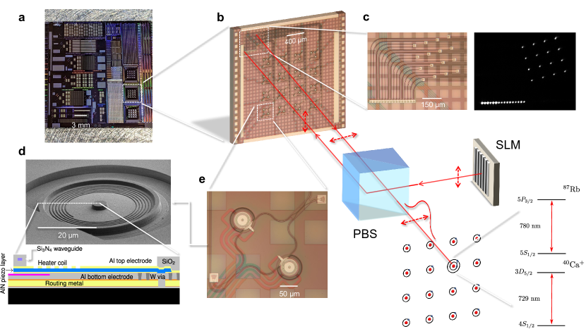
The illustration in Fig. 1 shows our proof-of-concept APIC with an array of sixteen high-speed dual-ring-assisted Mach-Zehnder modulators (DRMZMs) [24] arranged in a 44 grid. We show that these DRMZMs can, in a fabrication-tolerant way, achieve voltage-programmable light extinction in a compact footprint, as required for high-fidelity quantum control devices with large channel counts. We demonstrate that the spread in ring resonant frequencies due to fabrication non-uniformity, a major issue in large-scale PICs [25], can be eliminated using integrated thermo-optic heaters for tuning. Moreover, power dissipation from such tuning can be avoided by permanently shifting the resonances via laser-based trimming.
I Results
Interfacing between the laser source and the APIC is a large programmable switch to uniformly distribute light into each DRMZM (Fig. 1): in this case, implemented holographically via a commercial megapixel liquid crystal spatial light modulator (SLM) [26]. While such SLMs—with 100 update rate—cannot satisfy the speed criterion (C5) directly, they are ideal for static optical power fanout to balance light across the high speed DRMZMs in a scalable and reconfigurable way. By delegating the input light control to the millions of stable degrees-of-freedom on the SLM, we save the need for large-footprint, carefully-balanced, fabrication-sensitive splitter trees [27].
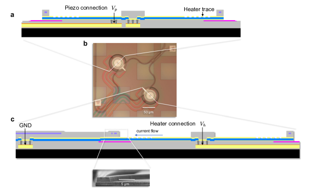
Vertically radiating gratings couple the holographically-distributed light into and out of each DRMZM. We route the inputs and outputs of the modulators together in one corner of the APIC (Fig. 1c), where we use a 116 array of grating couplers for coupling in, and a two-dimensional 44 array of grating couplers for coupling the modulated light out towards the target atomic systems. Notably, the input and output grating couplers are oriented at with respect to each other, such that a polarising beamsplitter (PBS) can be used to separate the in- and out- going light. At the system level, a relevant characteristic is the optical power efficiency of each device , where is the field amplitude at the input and output of a DRMZM and is applied voltage (Fig. 2a). Inefficiency is dominated by losses in the grating couplers. To boost efficiency, we take advantage of the aluminium layer underneath the grating which serves as the top piezo-electrode shown in Fig. 1d. The reflective aluminium directs light upward and greatly enhances coupling efficiency [28]. We achieve an approximate per-grating efficiency of and a total throughput of .
The large channel count criterion (C2) motivates high optical channel density . The resonant phase modulators used in the DRMZM afford a higher degree of compactness compared with conventional phase modulators. With an inter-device spacing of in our demonstrator cf. Fig. 1b, we achieve a device density of approximately six devices per square-millimetre . If we use the entire reticle () for our array, 2900 devices can be realised, with further improvements to compactness possible.
Performance metrics for quantum gates. We now establish key performance metrics of our device. These metrics are guided by the application requirements for optical quantum control. The Rabi frequency of an optically driven atomic transition depends on the electrical field (transverse coordinates ) at the position of the atom. Experimentally, we measure the optical power using a photodiode , where . For simplicity we consider a rectangular control pulse with constant light intensity in the “on” state. The extinction is , where is the residual light intensity in the “off” state. We define the intensity normalised pulse error by . Given an intensity error , the “on” state error is proportional to the square of the intensity error. The “off” state error scales linearly with extinction (see supplementary section I and [29]). The requirements on and for low pulse error correspond to criteria (C3) and (C4).
Criterion (C5) for fast switching times follows from the need for many gate operations to be executed during the lifetime of the quantum state [30, 6, 31]. Typical gate durations are in the range of tens to hundreds of nanoseconds for single-qubit rotations or entangling gates for cold atom systems [32, 31], atom-like emitters in solids [33], and in the range of microseconds to milliseconds for trapped ion motional gates [7, 6].
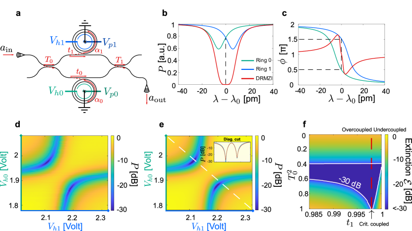
Modulator architecture. The DRMZM, schematically shown in Fig. 2a, lies at the core of our architecture. It consists of a Mach-Zehnder interferometer (MZI), with two 50:50 beamsplitters, and a ring resonator coupled to each arm of the interferometer.
Each ring resonator acts as a coupled phase and amplitude modulator with a well-known response function [34]:
| (1) |
where is the field amplitude at the input and output of a single ring, is the attenuation coefficient for a single round trip in the ring, is the bus waveguide’s self-coupling coefficient and is the round trip phase. For fast modulation, we rely on piezoelectric actuation cf. Fig. 4e. In the overcoupled regime (), the ring acts as a “force-multiplier” for phase, where the small phase shifts possible through the fast but weak piezoelectric actuators can be amplified to a phase shift per ring (Fig. 2c) [35]. Each ring is additionally equipped with a local heater (Fig. 1d) for long range tuning to compensate for fabrication variations (as discussed in the next section). Each overcoupled ring also modulates the amplitude in each arm of the MZI. By choosing the operating point of both rings correctly, we can select amplitude and phase in each arm to achieve in principle perfect destructive interference at the output port of the second beamsplitter. Furthermore, the two available degrees of freedom (phase tuning in both rings) afford full amplitude and phase control over the output electrical field (see supplementary section II). This full field control is especially desirable in protocols where the phase of the optical field needs to be changed quickly [36].
The simulated phase and amplitude response for both the isolated rings and the DRMZM is shown in Fig. 2b and c as a function of wavelength, assuming the ideal situation where the beamsplitters and rings are identical. We achieve perfect extinction at the output port when the differential phase is and the light amplitude in both MZI arms are exactly balanced to match the amplitude splitting ratio of the out-coupling beamsplitter. Fig. 2d shows the experimentally-measured output light power as a function of the heater voltages for each ring, which are used for long-range tuning to this ideal operating point. The points of minimum power are clearly visible in both branches of the “avoided crossing” of the two resonances ( in top branch and in bottom branch). We fit the experimental data to a model with parameters defined in Fig. 2a. The result is shown in Fig. 2e, in good agreement with the measured data ().
DRMZM extinction—a critical figure-of-merit for (C3)—is robust to large fabrication variations, in contrast to regular MZMs. In MZMs, the principal limitation to the achievable light extinction is given by how well the two beamsplitters comprising the MZM are matched to each other. Unequal beamsplitter ratios in the DRMZM are manifest in the output power distribution (Fig. 2e) as a breaking of mirror symmetry along the diagonal. The two points of minimum power translate along both branches as the difference between the beamsplitters increases. In Fig. 2f we show that a high extinction is achievable for a wide range of fabricated parameters. In our case, we attribute the primary limitations to the measured extinction ratio to originate from small drifts of the resonance position during the measurement along with input polarisation misalignment.
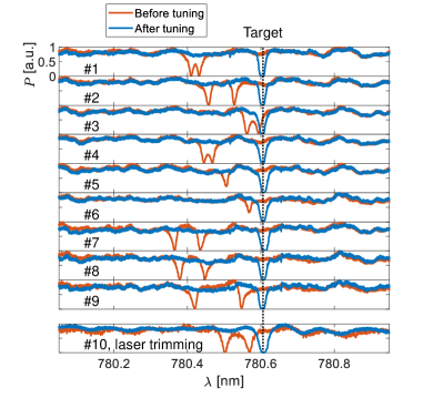
Resonance tuning. Fabrication-induced variations in resonance frequency are a major issue in integrated photonic devices [25]. While our piezoelectric actuators are fast, their range is not sufficient to account for this fabrication-induced resonance spread. In our system, as-fabricated resonances are distributed over hundreds of picometers or tens of linewidths, making modulation of a single laser frequency across the full array of devices impossible. To retune the system to a common resonance, we developed a combination of tunable and nonvolatile resonance shifting based on (i) integrated heaters [37] and (ii) laser trimming [38, 39, 40]. Fig. 3 plots the resonance positions for ten different DRMZMs before and after alignment.
For reconfigurable thermo-optic tuning, heating power is generated by a resistive coil in proximity of the waveguide, as shown in Fig. 1d. We measure resonance tuning efficiencies of (see supplementary section IV). Negating fabrication spread requires only moderate powers, on the order of per ring.
To complement thermal tuning and relax requirements on dissipated power, we can permanently but non-reversibly shift resonances by trimming rings with a blue laser, notably without degradation of the optical quality factor (see supplementary section V). The accessible trimming range is larger than the observed variations in resonance positions, and operates with sufficient precision to target within the limited range of piezoelectric actuation.
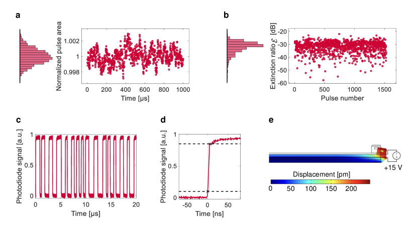
Fast switching. With resonances aligned at a desired operating point, we next demonstrate that our DRMZMs operate as fast light modulators with repeatable switching at high extinction ratios under piezoelectric actuation (C3-C5). Fig. 4a plots the measured normalised individual pulse area for a rectangular pulse train of total duration. This measurement indicates a pulse area consistency with a () standard deviation of (C4). Fig. 4d shows the fast switching behaviour of our device (C5). We observe a 10- rise time of . Further, we demonstrate a high extinction ratio of during switching (C3). Fig. 4b shows the extinction ratios for a pulse sequence with randomized pulse lengths (between and ), as displayed in Fig. 4c (see supplementary section III for eye diagrams). Table 1 summarises key performance metrics.
II Discussion
We introduced a SiN Atom-control Photonic Integrated Circuit (APIC) technology for scalable quantum control of atomic systems. Fabricated in a 200 mm wafer, CMOS-compatible process, our APICs achieve pulse errors of , extinction ratios , and rise times of , enabling high precision optical manipulation of quantum states. Furthermore, we showed that the fabrication-induced variations in resonance frequencies can be compensated for by integrated heaters or nonvolatile laser trimming, an essential feature for large-scale resonant PICs. The CMOS-compatiblity of our fabrication process also enables us to manufacture our photonics architecture directly on top of a high-voltage CMOS driver [41]. There are no fundamental limits to scaling our approach to thousands of channels in such an architecture. While we demonstrated operation at around , our architecture is compatible with operation across the entire transparency window of SiN down to blue wavelengths. Replacing SiN with wide-bandgap waveguiding materials such as aluminium oxide [42] or nitride [8] could enable operation down to UV wavelengths.
We anticipate that programmable optical control as achieved by our APIC platform will find widespread application for manipulating quantum systems, especially for atomic quantum control on arrays of neutral atoms [3, 4, 43, 9] or ions [6, 7]. In simulated condensed matter systems [44] we anticipate that our architecture will enable experimental studies beyond global many-body effects and towards local phenomena such as topological defects and their associated quasi-particles [45].
| Metric | Symbol | Value | Criterion |
|---|---|---|---|
| Wavelength | C1 | ||
| Channel density | C2 | ||
| Power efficiency | C2 | ||
| Extinction | C3 | ||
| Infidelity “off” state | C3 | ||
| Pulse error | C4 | ||
| Infidelity “on” state | C4 | ||
| 10- rise time | C5 |
III Methods
Device fabrication. Our devices are fabricated at Sandia National Laboratories on silicon wafers using deep ultraviolet optical lithography [20]. The devices have three metal layers interconnected through vias: a routing layer (Al/Ti), a bottom electrode layer (Al) and a top electrode layer (Al). A piezoelectric AlN layer sandwiched inbetween the bottom and top electrode layers enables piezoelectric actuators. The bottom and top electrode layers are connected to bond pads through vias and the bottom metal routing layer. On top of the piezoelectric actuators, a SiN waveguide layer ( thickness) is fabricated with silicon dioxide cladding above and below. An amorphous silicon release layer fabricated below the piezoelectric actuators can be used to undercut devices via \ceXeF2 etching [20]. The devices presented in this work are not released, to allow for a larger modulation bandwidth due to the “stiffer” resulting actuator. In Fig. 5 the on-chip electrical routing is illustrated.
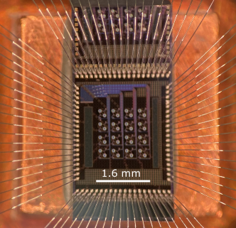
Packaging and drivers. After fabrication we dice the wafers into chips. The chips are glued on a copper block using a thermal epoxy. Wire bonds connect the chip to a printed circuit board (PCB). Fig. 6 shows a picture of the wire bonded chip. The PCB connects our chip to the heater and piezoelectric actuator drivers. The heaters are driven by Qontrol Q8iv modules delivering a maximum voltage of and a maximum current of (per channel). The piezoelectric actuators are driven by Spectrum M2p.6566-x4 arbitrary waveform generators with a maximum output rate of and an output level of into . This signal is amplified by a factor of five to using high-bandwidth electronic amplifiers (Texas Instruments THS3491) on the PCB, fed by a power supply. The maximum slew rate of the amplifiers is .
Actuation efficiency. To enhance resonance stability, we strongly overcouple the rings (effectively broadening the linewidth), while ensuring that each ring can be actuated to phase over the voltage range of achieved by our amplifiers. Our measured actuation efficiency conforms with the previously demonstrated [20]. The driving voltage of our devices can be reduced by using enhanced piezo-materials such as scandium-doped AlN, which has a piezoelectric response that is up to 5 times larger than that of AlN [46]. We can also choose to operate at lower driving voltages at the expense of a reduced light efficiency, as lower driving voltages result in smaller resonance shifts.
Author contributions
AJM designed the photonic chips. AJM, DE and IC conceived the experiments. AJM, AH, TP and IC built the experimental setup. AJM and AH performed the data analysis and simulation. AH and AJM conducted the measurements with assistance from IC, TP, MD and HL. IC, TP and MZ developed the control software. MZ designed the electronic drivers. AJL fabricated the chips. HR performed numerical strain simulations. CL implemented the blue light trimming with assistance from AJM, IC and TP. AJM, AH, IC and DE wrote the manuscript with input from all authors. AJM, AH, GG, ME and DE supervised the project.
†These authors contributed equally.
Acknowledgements.
The authors acknowledge Christoper Panuski and Sivan Trajtenberg-Mills for contributions to theslmsuite software package https://github.com/QPG-MIT/slmsuite, along with Lilia Chan for designing the chassis and chip mount, and Kevin Dauphinais for designing the PCB of the electronic driver.
Declarations
AJM acknowledges support from the Feodor Lynen Research Fellowship of the Humboldt Foundation, the MITRE Moonshot program, the Defense Advanced Research Projects Agency ONISQ program and the Department of Energy Quantum Systems Accelerator (QSA). AH was supported by a Fellowship of the Belgian American Educational Foundation. IC acknowledges support from the National Defense Science and Engineering Graduate Fellowship Program and the National Science Foundation (NSF) award DMR-1747426. TP acknowledges support from the NSF Graduate Research Fellowship Program and the MIT Jacobs Presidential Fellowship.
References
- Arute et al. [2019] F. Arute, K. Arya, R. Babbush, D. Bacon, J. C. Bardin, R. Barends, R. Biswas, S. Boixo, F. G. S. L. Brandao, D. A. Buell, B. Burkett, Y. Chen, Z. Chen, B. Chiaro, R. Collins, W. Courtney, A. Dunsworth, E. Farhi, B. Foxen, A. Fowler, C. Gidney, M. Giustina, R. Graff, K. Guerin, S. Habegger, M. P. Harrigan, M. J. Hartmann, A. Ho, M. Hoffmann, T. Huang, T. S. Humble, S. V. Isakov, E. Jeffrey, Z. Jiang, D. Kafri, K. Kechedzhi, J. Kelly, P. V. Klimov, S. Knysh, A. Korotkov, F. Kostritsa, D. Landhuis, M. Lindmark, E. Lucero, D. Lyakh, S. Mandrà, J. R. McClean, M. McEwen, A. Megrant, X. Mi, K. Michielsen, M. Mohseni, J. Mutus, O. Naaman, M. Neeley, C. Neill, M. Y. Niu, E. Ostby, A. Petukhov, J. C. Platt, C. Quintana, E. G. Rieffel, P. Roushan, N. C. Rubin, D. Sank, K. J. Satzinger, V. Smelyanskiy, K. J. Sung, M. D. Trevithick, A. Vainsencher, B. Villalonga, T. White, Z. J. Yao, P. Yeh, A. Zalcman, H. Neven, and J. M. Martinis, Quantum supremacy using a programmable superconducting processor, Nature 574, 505 (2019).
- Zhong et al. [2020] H.-S. Zhong, H. Wang, Y.-H. Deng, M.-C. Chen, L.-C. Peng, Y.-H. Luo, J. Qin, D. Wu, X. Ding, Y. Hu, P. Hu, X.-Y. Yang, W.-J. Zhang, H. Li, Y. Li, X. Jiang, L. Gan, G. Yang, L. You, Z. Wang, L. Li, N.-L. Liu, C.-Y. Lu, and J.-W. Pan, Quantum computational advantage using photons, Science 370, 1460 (2020).
- Graham et al. [2022] T. M. Graham, Y. Song, J. Scott, C. Poole, L. Phuttitarn, K. Jooya, P. Eichler, X. Jiang, A. Marra, B. Grinkemeyer, M. Kwon, M. Ebert, J. Cherek, M. T. Lichtman, M. Gillette, J. Gilbert, D. Bowman, T. Ballance, C. Campbell, E. D. Dahl, O. Crawford, N. S. Blunt, B. Rogers, T. Noel, and M. Saffman, Multi-qubit entanglement and algorithms on a neutral-atom quantum computer, Nature 604, 457 (2022).
- Ebadi et al. [2021] S. Ebadi, T. T. Wang, H. Levine, A. Keesling, G. Semeghini, A. Omran, D. Bluvstein, R. Samajdar, H. Pichler, W. W. Ho, S. Choi, S. Sachdev, M. Greiner, V. Vuletić, and M. D. Lukin, Quantum phases of matter on a 256-atom programmable quantum simulator, Nature 595, 227 (2021).
- Debnath et al. [2016] S. Debnath, N. M. Linke, C. Figgatt, K. A. Landsman, K. Wright, and C. Monroe, Demonstration of a small programmable quantum computer with atomic qubits, Nature 536, 63 (2016).
- Bruzewicz et al. [2019] C. D. Bruzewicz, J. Chiaverini, R. McConnell, and J. M. Sage, Trapped-ion quantum computing: Progress and challenges, Applied Physics Reviews 6, 021314 (2019).
- Pino et al. [2021] J. M. Pino, J. M. Dreiling, C. Figgatt, J. P. Gaebler, S. A. Moses, M. S. Allman, C. H. Baldwin, M. Foss-Feig, D. Hayes, K. Mayer, C. Ryan-Anderson, and B. Neyenhuis, Demonstration of the trapped-ion quantum CCD computer architecture, Nature 592, 209 (2021).
- Wan et al. [2020] N. H. Wan, T.-J. Lu, K. C. Chen, M. P. Walsh, M. E. Trusheim, L. De Santis, E. A. Bersin, I. B. Harris, S. L. Mouradian, I. R. Christen, E. S. Bielejec, and D. Englund, Large-scale integration of artificial atoms in hybrid photonic circuits, Nature 583, 226 (2020).
- Abobeih et al. [2022] M. H. Abobeih, Y. Wang, J. Randall, S. J. H. Loenen, C. E. Bradley, M. Markham, D. J. Twitchen, B. M. Terhal, and T. H. Taminiau, Fault-tolerant operation of a logical qubit in a diamond quantum processor, Nature 606, 884– (2022).
- Omran et al. [2019] A. Omran, H. Levine, A. Keesling, G. Semeghini, T. T. Wang, S. Ebadi, H. Bernien, A. S. Zibrov, H. Pichler, S. Choi, J. Cui, M. Rossignolo, P. Rembold, S. Montangero, T. Calarco, M. Endres, M. Greiner, V. Vuletić, and M. D. Lukin, Generation and manipulation of Schrödinger cat states in Rydberg atom arrays, Science 365, 570 (2019).
- Wright et al. [2019] K. Wright, K. M. Beck, S. Debnath, J. M. Amini, Y. Nam, N. Grzesiak, J.-S. Chen, N. C. Pisenti, M. Chmielewski, C. Collins, K. M. Hudek, J. Mizrahi, J. D. Wong-Campos, S. Allen, J. Apisdorf, P. Solomon, M. Williams, A. M. Ducore, A. Blinov, S. M. Kreikemeier, V. Chaplin, M. Keesan, C. Monroe, and J. Kim, Benchmarking an 11-qubit quantum computer, Nature Communications 10, 5464 (2019).
- Rahim et al. [2021] A. Rahim, A. Hermans, B. Wohlfeil, D. Petousi, B. Kuyken, D. Van Thourhout, and R. Baets, Taking silicon photonics modulators to a higher performance level: state-of-the-art and a review of new technologies, Advanced Photonics 3, 024003 (2021).
- Rahim et al. [2018] A. Rahim, T. Spuesens, R. Baets, and W. Bogaerts, Open-access silicon photonics: Current status and emerging initiatives, Proceedings of the IEEE 106, 2313 (2018).
- Smit et al. [2019] M. Smit, K. Williams, and J. van der Tol, Past, present, and future of InP-based photonic integration, APL Photonics 4, 050901 (2019).
- Rahim et al. [2017] A. Rahim, E. Ryckeboer, A. Z. Subramanian, S. Clemmen, B. Kuyken, A. Dhakal, A. Raza, A. Hermans, M. Muneeb, S. Dhoore, Y. Li, U. Dave, P. Bienstman, N. Le Thomas, G. Roelkens, D. Van Thourhout, P. Helin, S. Severi, X. Rottenberg, and R. Baets, Expanding the silicon photonics portfolio with silicon nitride photonic integrated circuits, Journal of Lightwave Technology 35, 639 (2017).
- Morin et al. [2021] T. J. Morin, L. Chang, W. Jin, C. Li, J. Guo, H. Park, M. A. Tran, T. Komljenovic, and J. E. Bowers, CMOS-foundry-based blue and violet photonics, Optica 8, 755 (2021).
- Bauters et al. [2011] J. F. Bauters, M. J. R. Heck, D. D. John, J. S. Barton, C. M. Bruinink, A. Leinse, R. G. Heideman, D. J. Blumenthal, and J. E. Bowers, Planar waveguides with less than 0.1 dB/m propagation loss fabricated with wafer bonding, Optics Express 19, 24090 (2011).
- El Dirani et al. [2019] H. El Dirani, L. Youssef, C. Petit-Etienne, S. Kerdiles, P. Grosse, C. Monat, E. Pargon, and C. Sciancalepore, Ultralow-loss tightly confining Si3N4 waveguides and high- microresonators, Optics Express 27, 30726 (2019).
- Liang et al. [2021] G. Liang, H. Huang, A. Mohanty, M. C. Shin, X. Ji, M. J. Carter, S. Shrestha, M. Lipson, and N. Yu, Robust, efficient, micrometre-scale phase modulators at visible wavelengths, Nature Photonics 15, 908 (2021).
- Stanfield et al. [2019] P. R. Stanfield, A. J. Leenheer, C. P. Michael, R. Sims, and M. Eichenfield, CMOS-compatible, piezo-optomechanically tunable photonics for visible wavelengths and cryogenic temperatures, Optics Express 27, 28588 (2019).
- Tian et al. [2020] H. Tian, J. Liu, B. Dong, J. C. Skehan, M. Zervas, T. J. Kippenberg, and S. A. Bhave, Hybrid integrated photonics using bulk acoustic resonators, Nature Communications 11, 3073 (2020).
- Dong et al. [2022] M. Dong, G. Clark, A. J. Leenheer, M. Zimmermann, D. Dominguez, A. J. Menssen, D. Heim, G. Gilbert, D. Englund, and M. Eichenfield, High-speed programmable photonic circuits in a cryogenically compatible, visible–near-infrared 200 mm CMOS architecture, Nature Photonics 16, 59 (2022).
- Lee and Lipson [2013] Y. H. D. Lee and M. Lipson, Back-end deposited silicon photonics for monolithic integration on CMOS, IEEE Journal of Selected Topics in Quantum Electronics 19, 8200207 (2013).
- Wang et al. [2007] Z. Wang, S.-J. Chang, C.-Y. Ni, and Y. J. Chen, A high-performance ultracompact optical interleaver based on double-ring assisted Mach–Zehnder interferometer, IEEE Photonics Technology Letters 19, 1072 (2007).
- Bogaerts et al. [2014] W. Bogaerts, M. Fiers, and P. Dumon, Design challenges in silicon photonics, IEEE Journal of Selected Topics in Quantum Electronics 20, 8202008 (2014).
- Christen et al. [2022] I. Christen, M. Sutula, T. Propson, H. Sattari, G. Choong, C. Panuski, A. Melville, J. Mallek, S. Hamilton, P. B. Dixon, et al., An integrated photonic engine for programmable atomic control, arXiv preprint arXiv:2208.06732 (2022).
- Tao et al. [2008] S. H. Tao, Q. Fang, J. F. Song, M. B. Yu, G. Q. Lo, and D. L. Kwong, Cascade wide-angle Y-junction 1 × 16 optical power splitter based on silicon wire waveguides on silicon-on-insulator, Optics Express 16, 21456 (2008).
- Van Laere et al. [2007] F. Van Laere, G. Roelkens, M. Ayre, J. Schrauwen, D. Taillaert, D. Van Thourhout, T. F. Krauss, and R. Baets, Compact and highly efficient grating couplers between optical fiber and nanophotonic waveguides, Journal of Lightwave Technology 25, 151 (2007).
- Nielsen and Chuang [2002] M. A. Nielsen and I. Chuang, Quantum computation and quantum information (2002).
- Bernien et al. [2017] H. Bernien, S. Schwartz, A. Keesling, H. Levine, A. Omran, H. Pichler, S. Choi, A. S. Zibrov, M. Endres, M. Greiner, et al., Probing many-body dynamics on a 51-atom quantum simulator, Nature 551, 579 (2017).
- Morgado and Whitlock [2021] M. Morgado and S. Whitlock, Quantum simulation and computing with Rydberg-interacting qubits, AVS Quantum Science 3, 023501 (2021).
- Levine et al. [2019] H. Levine, A. Keesling, G. Semeghini, A. Omran, T. T. Wang, S. Ebadi, H. Bernien, M. Greiner, V. Vuletić, H. Pichler, and M. D. Lukin, Parallel implementation of high-fidelity multiqubit gates with neutral atoms, Physical Review Letters 123, 170503 (2019).
- Debroux et al. [2021] R. Debroux, C. P. Michaels, C. M. Purser, N. Wan, M. E. Trusheim, J. Arjona Martínez, R. A. Parker, A. M. Stramma, K. C. Chen, L. de Santis, E. M. Alexeev, A. C. Ferrari, D. Englund, D. A. Gangloff, and M. Atatüre, Quantum control of the tin-vacancy spin qubit in diamond, Physical Review X 11, 041041 (2021).
- Bogaerts et al. [2012] W. Bogaerts, P. De Heyn, T. Van Vaerenbergh, K. De Vos, S. Kumar Selvaraja, T. Claes, P. Dumon, P. Bienstman, D. Van Thourhout, and R. Baets, Silicon microring resonators, Laser & Photonics Reviews 6, 47 (2012).
- Gill et al. [2010] D. M. Gill, S. S. Patel, M. Rasras, K.-Y. Tu, A. E. White, Y.-K. Chen, A. Pomerene, D. Carothers, R. L. Kamocsai, C. M. Hill, and J. Beattie, CMOS-compatible Si-ring-assisted Mach–Zehnder interferometer with internal bandwidth equalization, IEEE Journal of Selected Topics in Quantum Electronics 16, 45 (2010).
- Zhang et al. [2012] X. L. Zhang, A. T. Gill, L. Isenhower, T. G. Walker, and M. Saffman, Fidelity of a Rydberg-blockade quantum gate from simulated quantum process tomography, Physical Review A 85, 042310 (2012).
- Huang et al. [2020] Y. Huang, Q. Cheng, Y.-H. Hung, H. Guan, X. Meng, A. Novack, M. Streshinsky, M. Hochberg, and K. Bergman, Multi-stage 8 × 8 silicon photonic switch based on dual-microring switching elements, Journal of Lightwave Technology 38, 194 (2020).
- Lipka et al. [2014] T. Lipka, M. Kiepsch, H. K. Trieu, and J. Müller, Hydrogenated amorphous silicon photonic device trimming by UV-irradiation, Optics Express 22, 12122 (2014).
- De Paoli et al. [2020] G. De Paoli, S. L. Jantzen, T. D. Bucio, I. Skandalos, C. Holmes, P. G. R. Smith, M. M. Milosevic, and F. Y. Gardes, Laser trimming of the operating wavelength of silicon nitride racetrack resonators, Photonics Research 8, 677 (2020).
- Panuski et al. [2022] C. L. Panuski, I. R. Christen, M. Minkov, C. J. Brabec, S. Trajtenberg-Mills, A. D. Griffiths, J. J. D. McKendry, G. L. Leake, D. J. Coleman, C. Tran, J. St Louis, J. Mucci, C. Horvath, J. N. Westwood-Bachman, S. F. Preble, M. D. Dawson, M. J. Strain, M. L. Fanto, and D. R. Englund, A full degree-of-freedom photonic crystal spatial light modulator, arXiv preprint arXiv:2204.10302 (2022).
- Johansson and Fritzin [2013] T. Johansson and J. Fritzin, A review of watt-level CMOS RF power amplifiers, IEEE transactions on microwave theory and techniques 62, 111 (2013).
- West et al. [2019] G. N. West, W. Loh, D. Kharas, C. Sorace-Agaskar, K. K. Mehta, J. Sage, J. Chiaverini, and R. J. Ram, Low-loss integrated photonics for the blue and ultraviolet regime, APL Photonics 4, 026101 (2019).
- Pezzagna and Meijer [2021] S. Pezzagna and J. Meijer, Quantum computer based on color centers in diamond, Applied Physics Reviews 8, 011308 (2021).
- Abanin et al. [2019] D. A. Abanin, E. Altman, I. Bloch, and M. Serbyn, Colloquium: Many-body localization, thermalization, and entanglement, Reviews of Modern Physics 91, 021001 (2019).
- Yan et al. [2021] Z. Yan, Y.-C. Wang, N. Ma, Y. Qi, and Z. Y. Meng, Topological phase transition and single/multi anyon dynamics of Z2 spin liquid, npj Quantum Materials 6, 1 (2021).
- Teshigahara et al. [2012] A. Teshigahara, K.-y. Hashimoto, and M. Akiyama, Scandium aluminum nitride: Highly piezoelectric thin film for RF SAW devices in multi GHz range, in IEEE International Ultrasonics Symposium (2012).