Non-Reciprocal Supercurrents in a Field-Free Graphene Josephson Triode
Abstract
Superconducting diodes are proposed non-reciprocal circuit elements that should exhibit non-dissipative transport in one direction while being resistive in the opposite direction. Multiple examples of such devices have emerged in the past couple of years, however their efficiency is typically limited, and most of them require magnetic field to function. Here we present a device achieving efficiencies upwards of 90% while operating at zero field. Our samples consist of a network of three graphene Josephson junctions linked by a common superconducting island, to which we refer as a Josephson triode. The triode is tuned by applying a control current to one of the contacts, thereby breaking the time-reversal symmetry of the current flow. The triode’s utility is demonstrated by rectifying a small (tens of nA amplitude) applied square wave. We speculate that devices of this type could be realistically employed in the modern quantum circuits.
I Introduction
Diodes form one of the most important building blocks in electronic circuits, since they can be used in AC-DC conversion, signal rectification, and photodetection. The utility of diodes resides in their ability to offer non-reciprocity – a low resistance to current flowing in one direction and a high resistance to current flowing in the opposite direction. While traditional diodes exploit P-N interfaces in semiconducting materials, a flurry of theoretical interest has focused on developing their superconducting analogues [1, 2, 3, 4, 5, 6, 7, 8].
While these studies have followed a decade-long explorations of non-reciprocal supercurrents [9, 10, 11, 12, 13, 14, 15, 16, 17, 18, 19], the recent interest is driven by the search of novel materials which break both the inversion and time-reversal symmetry, thereby intrinsically enabling the superconducting diode effect (SDE). Such materials have indeed been experimentally identified and investigated, ranging from metallic films and proximitized semiconductors to van der Waals heterostructures [20, 21, 22, 23, 24, 25, 26, 27, 28, 29, 30]. While this direction offers a probe into the symmetry properties of novel materials, the resulting devices typically have limited diode efficiency, which is defined as a ratio of supercurrent in the forward and backward directions.
In the meanwhile, it has been realized that higher superconducting diode efficiency can be achieved in properly designed nanostructures with an external magnetic field applied to break the time-reversal symmetry [31, 32, 33, 34, 35]. Unfortunately, magnetic field is often undesired for integrating the diodes in superconducting circuits. In this work, we rectify this problem by creating superconducting diodes which can operate at zero external magnetic field and achieve efficiency approaching 100%. Our devices are based on multiterminal Josephson junctions made in graphene. In the past few years, the multiterminal junctions have been realized in a variety of materials [36, 37, 38, 39, 40, 41] and have even found a foothold as a solution to technological problems [42, 43].
We utilize the developments of multi-terminal Josephson junction design to eliminate the necessity of an applied magnetic field to achieve the SDE. The structure is based on three graphene Josephson junctions tied at the central superconducting island (Fig. 1a). Without applying a DC offset bias, all junctions are superconducting and the curves are symmetric. By applying a dissipationless control current in one of the junctions, we break the time-reversal symmetry and tune the curves of the other two junctions, achieving the SDE efficiencies exceeding 90%. Our devices are further tunable by electrostatic gating [44], which allows us to adjust the scale the supercurrent that can be rectified.
II Results
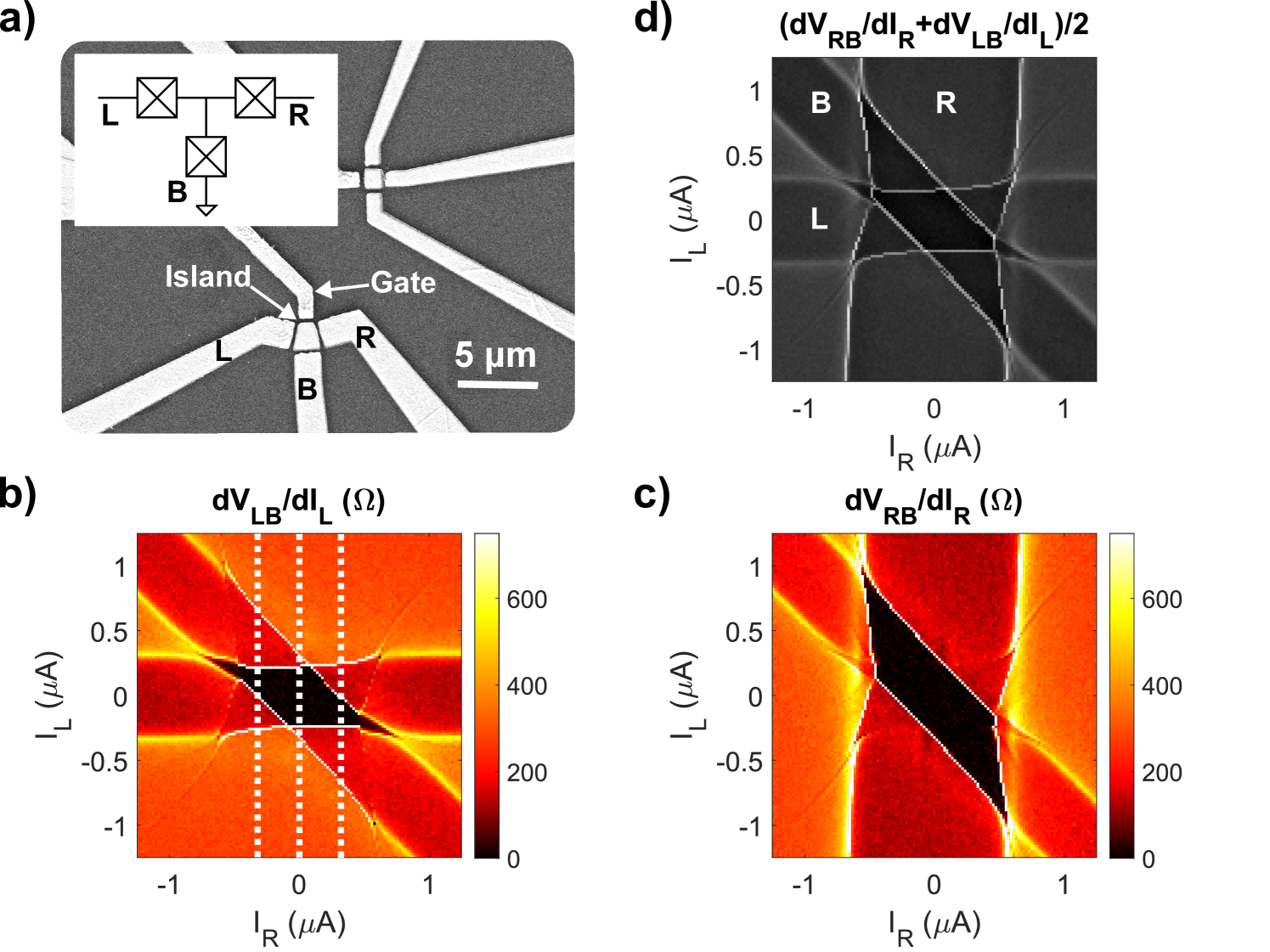
Our devices feature a trapezoidal superconducting island and three superconducting contacts labeled left (L), right (R) and bottom (B), Fig. 1a. (An additional side-gate approaching the island from the top does not contact the device and is not used in these measurements.) The contacts are connected to the island through 500 nm graphene channels which are etched such that none of the contacts are connected through graphene alone – all transport must occur through the central island. We have measured two devices which yielded very similar results. For consistency, we present the results for one of them, shown at the bottom of Fig. 1a.
The contacts and the island are made of sputtered molybdenum-rhenium (MoRe), which offers high-transparency Ohmic contact to graphene [45, 46]. The devices are cooled to a base temperature of 60 mK in a Leiden Cryogenics dilution refrigerator. A significant hysteresis is observed between the switching and retrapping currents, indicating either underdamping, or more likely electron overheating [47]. To avoid this hysteresis, the sample is heated to K for the measurements in Figs. 1-3. We have verified that all the features measured at this temperature range exhibit negligible hysteresis and can be measured by sweeping the current in any direction. DC currents and are applied to the left and right contacts with respect to the grounded bottom contact, and a small AC excitation is used for extracting differential resistances. To maximize the critical current, a back gate voltage of 20 V is applied in Figs. 1, 2, and 4. The Dirac point in this sample is at 2.5 V. Importantly, all measurements take place at zero magnetic field.
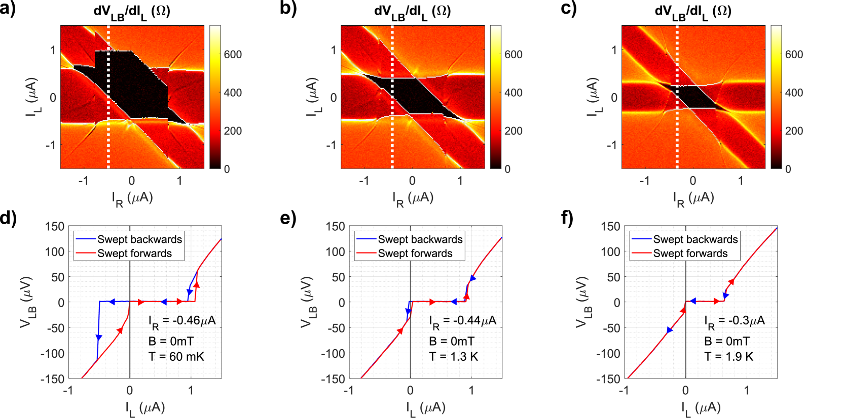
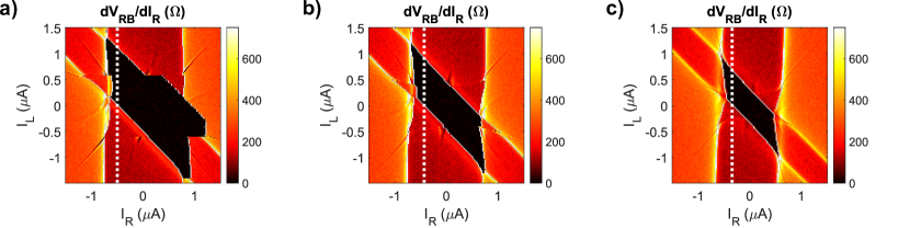
Fig. 1b and Fig. 1c correspond to the differential resistant maps measured between the left and bottom (1b) and right and bottom (1c) contacts. Correspondingly, the prominent horizontal (1b) and vertical (1c) features correspond to the regimes where respectively the left and right junctions are superconducting. The diagonal feature common to both maps corresponds to the bottom junction being superconducting. The device’s collective behavior can be gleaned from Fig. 1d where and are averaged. The distinct black region in the center of this map occurs where all three junctions are superconducting and the transport across the entire device is dissipationless.
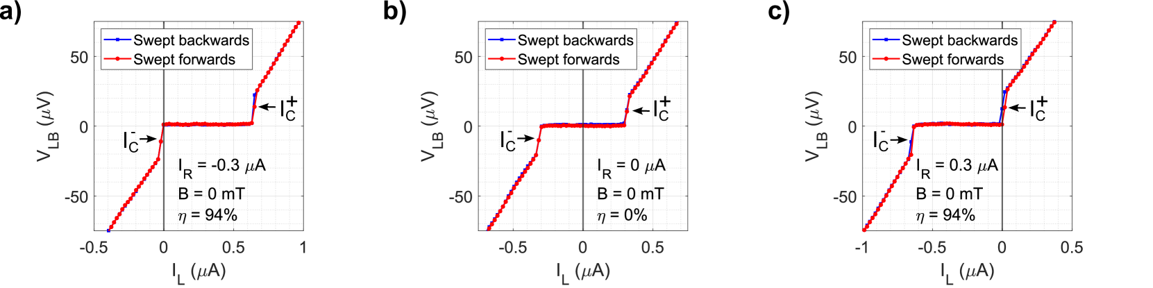
The boundaries of the dissipationless region (an uneven hexagon) correspond to points where at least one junction on the device switches to normal. The non-reciprocity we exploit here appears in the regions of the hexagon defined by the switching currents of two junctions. An example is the left dashed line in Fig. 1b, which cuts through the hexagonal region away from its center. As a result, the system stays dissipationless only for positive and becomes dissipative at negative (Fig. 2a). Note that all three junctions play a role in this this process: the bottom junction switches at while the left junction is responsible for the upper limit of the dissipationless range, ; finally, it is the biasing of the right junction which establishes the required asymmetry. For zero , one recovers a symmetric cross-section along the direction (central white line in Fig. 1b and Fig. 2b). Finally, at the opposite value of the control current (right dash line in Fig. 1b and Fig. 2c) the system stays dissipationless only at negative and the curves are reversed compared to Fig. 2a. Note that the right junction is biased below its critical current in all three cases.
Collectively, the boundaries of the hexagon enable tuning of the transport non-reciprocity between any pair of contacts by adjusting the current applied to the third contact. This leads to a diode efficiency,
| (1) |
that in practice can be tuned to exceed 90%, as will be seen in Fig. 2, where we plot the curves corresponding to the three cross-sections in Fig. 1b. Each set of curves is measured in both directions, showing negligible hysteresis. When (Fig. 2b) the curves are expectedly symmetric, so and . However, as is tuned away from zero, the non-reciprocity grows and increases until it reaches at .
Further increase of is possible by applying higher . In fact, formally can exceed unity when becomes positive (same sign as ). However, this regime should be avoided if we are interested in rectifying small currents. Hence we stop increasing at the point where the high slope “knee” of the curve approaches the point . We then define conservatively as a point at half the slope of the knee (see arrow in Fig. 2a), resulting in the . Finally, either positive (Fig. 2a) or negative (Fig. 2c) currents can be rectified depending on the desired operation.
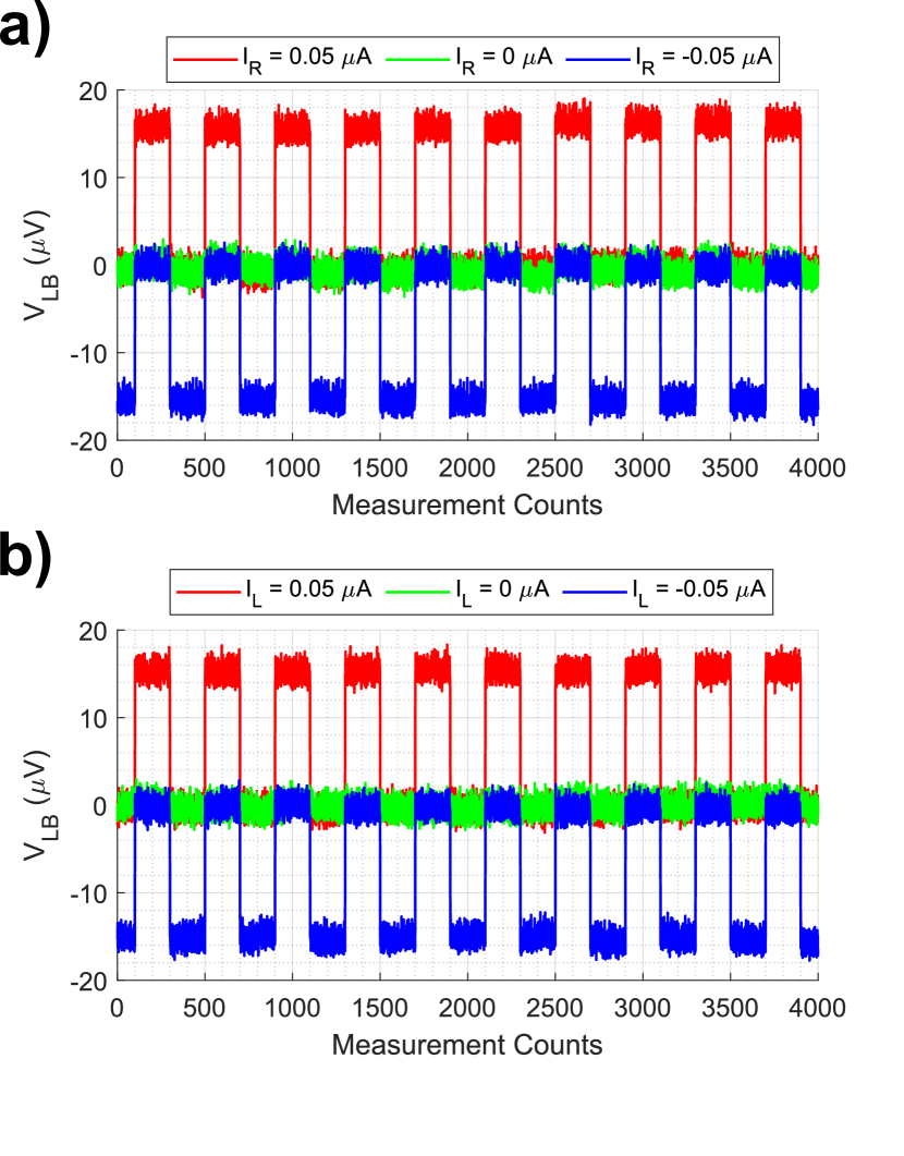
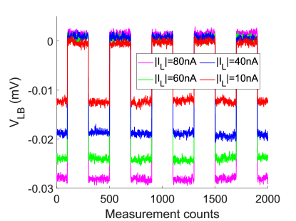
To demonstrate the potential utility of the device in quantum circuits, we decrease the gate voltage to zero and apply a square wave of amplitude 60 nA to the left contact (Fig. 3a). can then be set to produce desirable device responses: namely, at and nA, the negative and positive portions of the square wave are respectively rectified. Further, when = 0, the device is fully superconducting for the entire square wave, as its amplitude is smaller than the critical current of the device. As a result, the entire square wave passes through the device without dissipation. Interestingly, we can change the biasing scheme to further utilize the triode’s three-terminal nature. In Fig. 3b, we continue measuring but now use as a control parameter, while applying a square wave to . As a result, the voltage at the left contact, , switches depending on the sign of the square wave applied to the right contact.
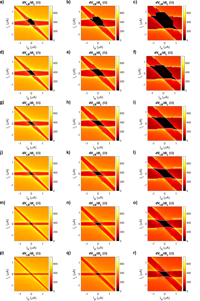
Fig. 4 explores the behavior of the sample as a function of temperature. The top row demonstrates the effect of temperature on the map of vs , first shown in Fig. 1. At the base temperature of 60 mK (Fig. 4a), the hysteresis is evident as the central superconducting pocket is shifted upward in the sweep direction. This hysteresis is still evident but much reduced at 1.3K (Fig. 4b), and finally it is clearly absent at 1.9 K (Fig. 4c). This is important, as hysteresis would prevent the diode from properly rectifying small currents. The bottom row presents the curves, measured at the same three temperatures with the adjusted to optimally tune the diode efficiency. (The values of are indicated as white lines across the corresponding maps.) Again, pronounced hysteresis is observed at the lowest temperature, but it is almost gone at 1.3 K, while the upper switching current, A, is not much suppressed compared to the lowest temperature. Further optimisation may result in suppressing the hysteresis at the base temperature. However, even the present device could be placed at the still plate of the dilution refrigerator to efficiently rectify a range of currents in the A range.
Interestingly, at base temperature, the central superconducting region deviates from the diamond present at elevated temperatures. In this state, nonlinear boundaries of the dissipationless region emerge – boundaries where a small amount of additional current on one contact could switch the device while a larger change in current would be required on the other contact. Along such boundaries, true transistor-like amplification could be envisioned.
III Discussion
While the near perfect diode efficiency of our device is compelling, integration into quantum circuits may be fundamentally limited the frequency cutoff and the fluctuations in the diode efficiency.
The frequency cutoff is limited by the RC time constant of the device. In the present case, this can be estimated by taking the normal resistance of the graphene junction ( 500 ) and the capacitance of the bonding pads and leads to the silicon backgate ( pF). Therefore, our present cutoff frequency could be as high as 1 GHz, indicating the promise for integrating our device into superconducting quantum circuits. Further improvements can be straightforwardly made by replacing the doped Si/SiO2 substrate with undoped Si and moving to local gating schemes. This would greatly decrease the parasitic capacitance, especially when using the triode on-chip with the rest of the circuit.
Turning to the fluctuations of the diode efficiency, the noise of the DC control bias could be an important source. As this bias fluctuates, the diode will pick up slight changes of , causing fluctuations of . While in this measurement we have not optimized the current noise beyond reasonably acceptable levels, we have been able to limit it below nA in the past [48]. In principle the noise in the diode could be pushed down to the quantum limit, where it is dominated by critical current fluctuations [49].
IV Conclusion
In summary, we utilize a network of three Josephson junctions at zero magnetic field to produce a superconducting diode with efficiency exceeding 90%. The device geometry – three graphene junctions connected by a common superconducting island – provides high degree of control through applied currents and gate voltage. While this device is made fairly simply in graphene, one can imagine copying the same Josephson circuit in other materials, including Al/Al2O3 tunnel junctions. Although in that case the gate tunability would be lost, the advantage is that the fabrication techniques are well developed and easily scalable. Further effort in this direction could quickly present opportunities for including high-efficiency superconducting diodes in quantum circuits.
V Methods
The sample is fabricated using standard techniques in exfoliation, stacking, and electron-beam lithography. The device is etched with ChF3O2 and SF6 plasma and contacts are deposited from sputtered molybdenum-rhenium (MoRe).
Measurements were conducted in a Leiden Cryogenics dilution refrigerator at a base sample temperature of 60 mK. Two stage 1.5 k/1 nF RC filters are mounted at the mixing chamber. Current bias passed through 1 M room temperature resistors, and voltage is measured with 1 nV homemade amplifiers. Interfacing with computer is performed with an NI USB-6363 DAQ board for both current biasing and voltage readouts.
To produce differential resistance maps as in Figure 1, the current bias on one contact is stepped in individual steps in an outer loop, while the bias on the other contact is swept quickly. From here, numerical derivatives can easily be computed to give resistance values (). Currents are ramped in both directions (e.g. A to 1.5 A and back to A) and all derivatives are computed (e.g. as well as ) so several maps can be produced for each measurement.
VI Acknowledgements
We thank K.C. Fong for helpful discussions. Transport measurements by J.C., E.G.A., T.F.Q.L. and C.C., and data analysis by J.C., E.G.A., and G.F., were supported by Division of Materials Sciences and Engineering, Office of Basic Energy Sciences, U.S. Department of Energy, under Award No. DE-SC0002765. Sample fabrication and characterization by E.G.A. and L.Z. was supported by the NSF Award DMR-2004870. F.A. was supported by a URC grant at Appalachian State University. K.W. and T.T. acknowledge support from JSPS KAKENHI (Grant Numbers 19H05790, 20H00354 and 21H05233). The sample fabrication was performed in part at the Duke University Shared Materials Instrumentation Facility (SMIF), a member of the North Carolina Research Triangle Nanotechnology Network (RTNN), which is supported by the National Science Foundation (Grant ECCS-1542015) as part of the National Nanotechnology Coordinated Infrastructure (NNCI).
References
- Zhang et al. [2022] Y. Zhang, Y. Gu, P. Li, J. Hu, and K. Jiang, General theory of josephson diodes (2022), arXiv:2112.08901 [cond-mat.supr-con] .
- Yuan and Fu [2022] N. F. Q. Yuan and L. Fu, Supercurrent diode effect and finite-momentum superconductors, Proceedings of the National Academy of Sciences 119, 10.1073/pnas.2119548119 (2022).
- He et al. [2022] J. J. He, Y. Tanaka, and N. Nagaosa, A phenomenological theory of superconductor diodes, New Journal of Physics 24, 053014 (2022).
- Daido et al. [2022] A. Daido, Y. Ikeda, and Y. Yanase, Intrinsic superconducting diode effect, Physical Review Letters 128, 10.1103/physrevlett.128.037001 (2022).
- Ilić and Bergeret [2022] S. Ilić and F. Bergeret, Theory of the supercurrent diode effect in rashba superconductors with arbitrary disorder, Physical Review Letters 128, 10.1103/physrevlett.128.177001 (2022).
- Halterman et al. [2022] K. Halterman, M. Alidoust, R. Smith, and S. Starr, Supercurrent diode effect, spin torques, and robust zero-energy peak in planar half-metallic trilayers, Physical Review B 105, 10.1103/physrevb.105.104508 (2022).
- Scammell et al. [2022] H. D. Scammell, J. I. A. Li, and M. S. Scheurer, Theory of zero-field superconducting diode effect in twisted trilayer graphene, 2D Materials 9, 025027 (2022).
- Davydova et al. [2022] M. Davydova, S. Prembabu, and L. Fu, Universal josephson diode effect (2022), arXiv:2201.00831 [cond-mat.supr-con] .
- Reynoso et al. [2008] A. A. Reynoso, G. Usaj, C. A. Balseiro, D. Feinberg, and M. Avignon, Anomalous josephson current in junctions with spin polarizing quantum point contacts, Physical Review Letters 101, 10.1103/physrevlett.101.107001 (2008).
- Zazunov et al. [2009] A. Zazunov, R. Egger, T. Jonckheere, and T. Martin, Anomalous josephson current through a spin-orbit coupled quantum dot, Physical Review Letters 103, 10.1103/physrevlett.103.147004 (2009).
- Reynoso et al. [2012] A. A. Reynoso, G. Usaj, C. A. Balseiro, D. Feinberg, and M. Avignon, Spin-orbit-induced chirality of andreev states in josephson junctions, Physical Review B 86, 10.1103/physrevb.86.214519 (2012).
- Yokoyama et al. [2013] T. Yokoyama, M. Eto, and Y. V. Nazarov, Josephson current through semiconductor nanowire with spin–orbit interaction in magnetic field, Journal of the Physical Society of Japan 82, 054703 (2013).
- Brunetti et al. [2013] A. Brunetti, A. Zazunov, A. Kundu, and R. Egger, Anomalous josephson current, incipient time-reversal symmetry breaking, and majorana bound states in interacting multilevel dots, Physical Review B 88, 10.1103/physrevb.88.144515 (2013).
- Silaev et al. [2014] M. A. Silaev, A. Y. Aladyshkin, M. V. Silaeva, and A. S. Aladyshkina, The diode effect induced by domain-wall superconductivity, Journal of Physics: Condensed Matter 26, 095702 (2014).
- Yokoyama et al. [2014] T. Yokoyama, M. Eto, and Y. V. Nazarov, Anomalous josephson effect induced by spin-orbit interaction and zeeman effect in semiconductor nanowires, Physical Review B 89, 10.1103/physrevb.89.195407 (2014).
- Dolcini et al. [2015] F. Dolcini, M. Houzet, and J. S. Meyer, Topological josephson junctions, Physical Review B 92, 10.1103/physrevb.92.035428 (2015).
- Hoshino et al. [2018] S. Hoshino, R. Wakatsuki, K. Hamamoto, and N. Nagaosa, Nonreciprocal charge transport in two-dimensional noncentrosymmetric superconductors, Physical Review B 98, 10.1103/physrevb.98.054510 (2018).
- Wakatsuki and Nagaosa [2018] R. Wakatsuki and N. Nagaosa, Nonreciprocal current in noncentrosymmetric rashba superconductors, Physical Review Letters 121, 10.1103/physrevlett.121.026601 (2018).
- Chen et al. [2018] C.-Z. Chen, J. J. He, M. N. Ali, G.-H. Lee, K. C. Fong, and K. T. Law, Asymmetric josephson effect in inversion symmetry breaking topological materials, Physical Review B 98, 10.1103/physrevb.98.075430 (2018).
- Wakatsuki et al. [2017] R. Wakatsuki, Y. Saito, S. Hoshino, Y. M. Itahashi, T. Ideue, M. Ezawa, Y. Iwasa, and N. Nagaosa, Nonreciprocal charge transport in noncentrosymmetric superconductors, Science Advances 3, 10.1126/sciadv.1602390 (2017).
- Ando et al. [2020] F. Ando, Y. Miyasaka, T. Li, J. Ishizuka, T. Arakawa, Y. Shiota, T. Moriyama, Y. Yanase, and T. Ono, Observation of superconducting diode effect, Nature 584, 373 (2020).
- Diez-Merida et al. [2021] J. Diez-Merida, A. Diez-Carlon, S. Y. Yang, Y. M. Xie, X. J. Gao, K. Watanabe, T. Taniguchi, X. Lu, K. T. Law, and D. K. Efetov, Magnetic josephson junctions and superconducting diodes in magic angle twisted bilayer graphene (2021), arXiv:2110.01067 [cond-mat.supr-con] .
- Shin et al. [2021] J. Shin, S. Son, J. Yun, G. Park, K. Zhang, Y. J. Shin, J.-G. Park, and D. Kim, Magnetic proximity-induced superconducting diode effect and infinite magnetoresistance in van der waals heterostructure (2021), arXiv:2111.05627 [cond-mat.supr-con] .
- Baumgartner et al. [2021] C. Baumgartner, L. Fuchs, A. Costa, S. Reinhardt, S. Gronin, G. C. Gardner, T. Lindemann, M. J. Manfra, P. E. F. Junior, D. Kochan, J. Fabian, N. Paradiso, and C. Strunk, Supercurrent rectification and magnetochiral effects in symmetric josephson junctions, Nature Nanotechnology 17, 39 (2021).
- Lin et al. [2022] J.-X. Lin, P. Siriviboon, H. D. Scammell, S. Liu, D. Rhodes, K. Watanabe, T. Taniguchi, J. Hone, M. S. Scheurer, and J. I. A. Li, Zero-field superconducting diode effect in small-twist-angle trilayer graphene (2022), arXiv:2112.07841 [cond-mat.mes-hall] .
- Wu et al. [2022] H. Wu, Y. Wang, Y. Xu, P. K. Sivakumar, C. Pasco, U. Filippozzi, S. S. P. Parkin, Y.-J. Zeng, T. McQueen, and M. N. Ali, The field-free josephson diode in a van der waals heterostructure, Nature 604, 653 (2022).
- Strambini et al. [2022] E. Strambini, M. Spies, N. Ligato, S. Ilić, M. Rouco, C. González-Orellana, M. Ilyn, C. Rogero, F. S. Bergeret, J. S. Moodera, P. Virtanen, T. T. Heikkilä, and F. Giazotto, Superconducting spintronic tunnel diode, Nature Communications 13, 10.1038/s41467-022-29990-2 (2022).
- Narita et al. [2022] H. Narita, J. Ishizuka, R. Kawarazaki, D. Kan, Y. Shiota, T. Moriyama, Y. Shimakawa, A. V. Ognev, A. S. Samardak, Y. Yanase, and T. Ono, Field-free superconducting diode effect in noncentrosymmetric superconductor/ferromagnet multilayers, Nature Nanotechnology 17, 823 (2022).
- Bauriedl et al. [2022] L. Bauriedl, C. Bäuml, L. Fuchs, C. Baumgartner, N. Paulik, J. M. Bauer, K.-Q. Lin, J. M. Lupton, T. Taniguchi, K. Watanabe, C. Strunk, and N. Paradiso, Supercurrent diode effect and magnetochiral anisotropy in few-layer NbSe2, Nature Communications 13, 10.1038/s41467-022-31954-5 (2022).
- Pal et al. [2022] B. Pal, A. Chakraborty, P. K. Sivakumar, M. Davydova, A. K. Gopi, A. K. Pandeya, J. A. Krieger, Y. Zhang, M. Date, S. Ju, N. Yuan, N. B. M. Schröter, L. Fu, and S. S. P. Parkin, Josephson diode effect from cooper pair momentum in a topological semimetal, Nature Physics 10.1038/s41567-022-01699-5 (2022).
- Lyu et al. [2021] Y.-Y. Lyu, J. Jiang, Y.-L. Wang, Z.-L. Xiao, S. Dong, Q.-H. Chen, M. V. Milošević, H. Wang, R. Divan, J. E. Pearson, P. Wu, F. M. Peeters, and W.-K. Kwok, Superconducting diode effect via conformal-mapped nanoholes, Nature Communications 12, 10.1038/s41467-021-23077-0 (2021).
- Souto et al. [2022] R. S. Souto, M. Leijnse, and C. Schrade, The josephson diode effect in supercurrent interferometers (2022), arXiv:2205.04469 [cond-mat.mes-hall] .
- Golod and Krasnov [2022] T. Golod and V. M. Krasnov, Demonstration of a superconducting diode-with-memory, operational at zero magnetic field with switchable nonreciprocity, Nature Communications 13, 10.1038/s41467-022-31256-w (2022).
- Gupta et al. [2022] M. Gupta, G. V. Graziano, M. Pendharkar, J. T. Dong, C. P. Dempsey, C. Palmstrøm, and V. S. Pribiag, Superconducting diode effect in a three-terminal josephson device (2022), arXiv:2206.08471 [cond-mat.mes-hall] .
- Fominov and Mikhailov [2022] Y. V. Fominov and D. S. Mikhailov, Asymmetric higher-harmonic squid as a josephson diode (2022), arXiv:2208.10856 [cond-mat.supr-con] .
- Strambini et al. [2016] E. Strambini, S. D'Ambrosio, F. Vischi, F. S. Bergeret, Y. V. Nazarov, and F. Giazotto, The -squipt as a tool to phase-engineer josephson topological materials, Nature Nanotechnology 11, 1055 (2016).
- Draelos et al. [2019] A. W. Draelos, M.-T. Wei, A. Seredinski, H. Li, Y. Mehta, K. Watanabe, T. Taniguchi, I. V. Borzenets, F. Amet, and G. Finkelstein, Supercurrent Flow in Multiterminal Graphene Josephson Junctions, Nano Letters 19, 1039 (2019).
- Graziano et al. [2020] G. V. Graziano, J. S. Lee, M. Pendharkar, C. J. Palmstrøm, and V. S. Pribiag, Transport studies in a gate-tunable three-terminal josephson junction, Physical Review B 101, 10.1103/physrevb.101.054510 (2020).
- Pankratova et al. [2020] N. Pankratova, H. Lee, R. Kuzmin, K. Wickramasinghe, W. Mayer, J. Yuan, M. G. Vavilov, J. Shabani, and V. E. Manucharyan, Multiterminal josephson effect, Physical Review X 10, 10.1103/physrevx.10.031051 (2020).
- Arnault et al. [2022] E. G. Arnault, S. Idris, A. McConnell, L. Zhao, T. F. Larson, K. Watanabe, T. Taniguchi, G. Finkelstein, and F. Amet, Dynamical stabilization of multiplet supercurrents in multiterminal josephson junctions, Nano Letters 22, 7073 (2022).
- Graziano et al. [2022] G. V. Graziano, M. Gupta, M. Pendharkar, J. T. Dong, C. P. Dempsey, C. Palmstrøm, and V. S. Pribiag, Selective control of conductance modes in multi-terminal josephson junctions (2022), arXiv:2201.01373 [ond-mat.mes-hall] .
- Uri et al. [2016] A. Uri, A. Y. Meltzer, Y. Anahory, L. Embon, E. O. Lachman, D. Halbertal, N. HR, Y. Myasoedov, M. E. Huber, A. F. Young, and E. Zeldov, Electrically tunable multiterminal SQUID-on-tip, Nano Letters 16, 6910 (2016).
- Lee et al. [2020] G.-H. Lee, D. K. Efetov, W. Jung, L. Ranzani, E. D. Walsh, T. A. Ohki, T. Taniguchi, K. Watanabe, P. Kim, D. Englund, and K. C. Fong, Graphene-based josephson junction microwave bolometer, Nature 586, 42 (2020).
- [44] See Supplementary information.
- Calado et al. [2015] V. E. Calado, S. Goswami, G. Nanda, M. Diez, A. R. Akhmerov, K. Watanabe, T. Taniguchi, T. M. Klapwijk, and L. M. K. Vandersypen, Ballistic Josephson junctions in edge-contacted graphene., Nature nanotechnology 10, 761 (2015).
- Borzenets et al. [2016] I. V. Borzenets, F. Amet, C. T. Ke, A. W. Draelos, M. T. Wei, A. Seredinski, K. Watanabe, T. Taniguchi, Y. Bomze, M. Yamamoto, S. Tarucha, and G. Finkelstein, Ballistic graphene josephson junctions from the short to the long junction regimes, Phys. Rev. Lett. 117, 237002 (2016).
- Borzenets et al. [2013] I. V. Borzenets, U. C. Coskun, H. T. Mebrahtu, Y. V. Bomze, A. I. Smirnov, and G. Finkelstein, Phonon bottleneck in graphene-based josephson junctions at millikelvin temperatures, Phys. Rev. Lett. 111, 027001 (2013).
- Amet et al. [2016] F. Amet, C. T. Ke, I. V. Borzenets, J. Wang, K. Watanabe, T. Taniguchi, R. S. Deacon, M. Yamamoto, Y. Bomze, S. Tarucha, and G. Finkelstein, Supercurrent in the quantum hall regime, Science 352, 966 (2016).
- Haque et al. [2021] M. T. Haque, M. Will, M. Tomi, P. Pandey, M. Kumar, F. Schmidt, K. Watanabe, T. Taniguchi, R. Danneau, G. Steele, and P. Hakonen, Critical current fluctuations in graphene josephson junctions, Scientific Reports 11, 10.1038/s41598-021-99398-3 (2021).
I Supplementary Information
Supplementary Information for Non-Reciprocal Supercurrents in a Field-Free Graphene Josephson Triode
John Chiles1†*, Ethan G. Arnault1†, Chun-Chia Chen1, Trevyn F.Q. Larson1,
Lingfei Zhao1, Kenji Watanabe2, Takashi Taniguchi2,
François Amet3, Gleb Finkelstein1
1Department of Physics, Duke University, Durham, NC 27701, USA
2National Institute for Materials Science, Tsukuba, 305-0044, Japan
3Department of Physics and Astonomy, Appalachian State University, Boone, NC 28607, USA
† These authors contributed to this work equally
∗To whom correspondence should be addressed; E-mail: john.chiles@duke.edu
I.1 Methods
The sample is fabricated using standard techniques in exfoliation, stacking, and electron-beam lithography. The device is etched with ChF3O2 and SF6 plasma and contacts are deposited from sputtered molybdenum-rhenium (MoRe).
Measurements were conducted in a Leiden Cryogenics dilution refrigerator at a base sample temperature of 60 mK. Two stage 1.5 k/1 nF RC filters are mounted at the mixing chamber. Current bias passed through 1 M room temperature resistors, and voltage is measured with 1 nV homemade amplifiers. Interfacing with computer is performed with an NI USB-6363 DAQ board for both current biasing and voltage readouts.
To produce differential resistance maps as in Figure 1, the current bias on one contact is stepped in individual steps in an outer loop, while the bias on the other contact is swept quickly. From here, numerical derivatives can easily be computed to give resistance values (). Currents are ramped in both directions (e.g. A to 1.5 A and back to A) and all derivatives are computed (e.g. as well as ) so several maps can be produced for each measurement.
I.2 Extended Temperature and Gate Voltage Data
In Supplementary Figure 1, we present maps of as and are varied. The maps are measured at 60 mK (a), 1.3 K (b), and 1.9 K (c), corresponding to the analogous maps of in Figure 4 of the main text. The vertical dashed lines indicate the values of at which the cuts of Figure 4 were taken. It is clear that these values of are well below the critical current of the right junction, indicating dissipationless control. Hence, the whole triode operates in the dissipationless regime while for a given curve.
As initially presented in Figure 4 of the main text, the device can be operated at a range of applied gate voltages and temperatures. To explore the full range of the operating parameters, we stepped the back gate voltage between 0 V and 25 V in steps of 5 V, and stepped the sample temperature from 60 mK to 1.9 K in 6 steps. As a result, we have 72 bias-bias maps for both and . In the Supplementary Figure 2, we present the maps for , 10, and 20 V. It is visible that the hysteresis disappears between 0.5 and 1K depending on the gate voltage, allowing for optimal operating conditions. Further, as gate is swept, we can rectify either smaller AC signals (near the Dirac peak at 2.5 V) or larger AC signals far from the Dirac peak. Notably, the high contact transparency of the MoRe-graphene interface allows for operating the device with both electron and hole doping.
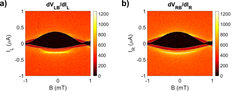
I.3 Behavior in Applied Magnetic Field
Supplemental Figure 3 shows the prototypical Fraunhofer patterns measure in perpendicular magnetic field for (a) at and (b) at . The patterns emerge as expected with the maximal switching current appearing at zero field. As expected, multiple lobes of the pattern are observed. As the junctions areas slightly vary, so do their field periodicities. Notably, in the second lobe there is a reduced overlap of the Fraunhofer patterns, causing a larger dark orange region where one of the junctions is turned normal by the field. Again, this feature is expected as slight offsets in the periodicity of the Fraunhofer pattern will compound at higher magnetic fields. This mismatch in periodicity may likely be the factor limiting the device performance at elevated field.
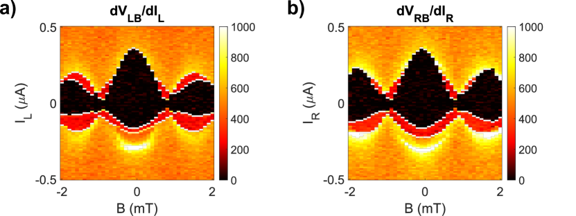
In Supplementary Figure 4, we show the Fraunhofer pattern with increased resolution. Note the region in both maps near 0.8 mT, where the dark orange corresponds to the bottom junction switching before either the left or right junction. Also, the current maxima are shifted from the nominal zero field by mT = Gs, which is within the expected range of the systematic error of the power supply. When measuring the data for the rest of the paper, we applied a nominal mT to stay at the true zero of magnetic field.
While the triode can be operated without the application of magnetic field, it may occur that the device has to be placed in an environment with some magnetic field offset. To this end, we show its performance at a small perpendicular field. In Supplementary Figure 5, we demonstrate a square wave rectification of the AC signal at 1 K and an applied field of 0.6 mT. Even at this elevated field, we are able to rectify ambipolar AC signals for a wide range of current amplitudes, thus demonstrating the device’s capability to work in the presence of a remnant or stray field.