Superconducting resonators with voltage-controlled frequency and nonlinearity
Abstract
Voltage-tunable superconductor-semiconductor devices offer a unique platform to realize dynamic tunability in superconducting quantum circuits. By galvanically connecting a gated InAs-Al Josephson junction to a coplanar waveguide resonator, we demonstrate the use of a superconducting element with wideband gate-tunability. We show that the resonant frequency is controlled via a gate-tunable Josephson inductance and that the non-linearity of the InAs-Al junction is non-dissipative as is the case with conventional AlO-Al junctions. As the gate voltage is decreased, the inductive participation of the junction increases up to , resulting in the resonant frequency being tuned by over . Utilizing the wide tunability of the device, we demonstrate that two resonant modes can be adjusted such that they strongly hybridize, exhibiting an avoided level crossing with a coupling strength of . Implementing such voltage-tunable resonators is the first step toward realizing wafer-scale continuous voltage control in superconducting circuits for qubit-qubit coupling, quantum-limited amplifiers, and quantum memory platforms.
I Introduction
Advances in materials growth, fabrication, and device design have paved the way for the success of superconducting quantum systems based on solid-state platforms Kjaergaard et al. (2020); Blais et al. (2021); Wallraff et al. (2004); Blais et al. (2004); Koch et al. (2007); Gyenis et al. (2021). Recently, fixed-frequency superconducting qubits have shown coherence times greater than 1 ms Place et al. (2020); Somoroff et al. (2021); however, static crosstalk and parasitic coupling limits two-qubit gate fidelity McKay et al. (2019). On the other hand, flux-tunable circuits have garnered attention for their ability to eliminate unwanted interactions Yan et al. (2018); Mundada et al. (2019); Sung et al. (2021); Foxen et al. (2020). In addition, they have allowed for fast ( ) high-fidelity () two-qubit gates Chen et al. (2014), as opposed to cross-resonance based gates which typically take 150-200 Sheldon et al. (2016); Kandala et al. (2021). These circuits are almost exclusively realized by flux-sensitive superconducting quantum interference devices (SQUIDs) Orlando et al. (1999); Chiorescu et al. (2003); Palacios-Laloy et al. (2008); Naaman et al. (2016); Chen et al. (2014). However, conventional flux-tunable circuits have qubit phase coherence limited by low-frequency flux noise Kakuyanagi et al. (2007); Hutchings et al. (2017); Kumar et al. (2016); Bialczak et al. (2007). Alternatively, superconductor-semiconductor hybrid structures can be employed to provide voltage tunability for fast and low-power control. The fast gate switching times offered by transistor-like device architectures could be utilized for high-speed coupling and two-qubit gates. In addition, the local control imposed by voltage-tunable devices can offer a flexible design feature for large-scale device footprints, inevitably adding new functionality to the superconducting qubit toolbox.
In a Josephson junction (JJ) with a semiconductor weak link, Cooper pair transport is facilitated by Andreev reflections at the superconductor-semiconductor interface Beenakker (1992). Multiple, coherent reflections form current-carrying Andreev bound states. As the Fermi energy tunes the occupation of each state, such as by an applied gate voltage , the total critical current can be controlled. Such tunability has been routinely demonstrated in current biased devices Mayer et al. (2019); Nichele et al. (2017); Suominen et al. (2017); Kjaergaard et al. (2017); Elfeky et al. (2021), and utilized in qubit manipulation, specifically with gatemon qubits de Lange et al. (2015); Larsen et al. (2015); Luthi et al. (2018); Kringhøj et al. (2018); Casparis et al. (2018, 2016); O’Connell Yuan et al. (2021); Larsen et al. (2020); Danilenko et al. (2022); Hertel et al. (2022). Furthermore, semiconductor weak-links can directly find applications in the form of couplers Casparis et al. (2019); Qi et al. (2018); Sardashti et al. (2020), amplifiers Phan et al. (2022a), superconductor-coupled quantum dot devices Casparis et al. (2018); Scarlino et al. (2019); Borjans et al. (2020); Burkard et al. (2020), Andreev qubits Hays et al. (2020, 2021) and nonreciprocal devices Leroux et al. (2022).
In this work, we present a wideband, wafer-scale implementation of a voltage-tunable resonator. The device is based on an InAs two-dimensional electron gas (2DEG) and contacted with epitaxial Al fabricated into a Josephson junction embedded in a coplanar waveguide (CPW) resonator. We show that the Josephson inductance is modified electrostatically by an order of magnitude, allowing for the resonant frequency to be tuned within a band. In addition, by studying the high power response of the device we find that the junction exhibits non-dissipative noninearity. The tunability of the resonator frequency allows for strong hybridization with another resonator on the chip. With a maximum coupling strength of , we achieve strong coupling between the two resonators.
II Device design
| Resonator | (mm) | (GHz) | (pF) | (nH) | |
|---|---|---|---|---|---|
| TR1 | 4.936 | 5.967 | 270 | 0.433 | 1.645 |
| TR2 | 4.136 | 7.111 | 201 | 0.363 | 1.380 |
| R3 | 4.536 | 6.491 | 180 | 0.398 | 1.512 |
| TR4 | 3.736 | 7.559 | 152 | 0.341 | 1.298 |
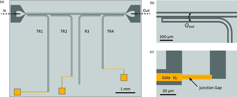
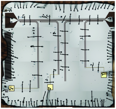
The devices are fabricated on a superconductor-semiconductor heterostructure grown via molecular beam epitaxy Shabani et al. (2016); Wickramasinghe et al. (2018); Yuan et al. (2020); Strickland et al. (2022); details of the growth are discussed in the Supplementary Material. The weak link of the JJ is a high-mobility InAs 2DEG grown near the surface and contacted in-situ by a thin aluminum film. The epitaxial heterostructure is grown on a thick InP substrate. We use a III-V wet etch to define the microwave circuit and an Al wet etch to define the JJ. The junction gap is long and wide. We then deposit a AlO gate dielectric, followed by a gate electrode made of layers of Cr and Au which are and respectively. A stitched optical image of the wirebonded device is shown in Supplementary Material in Fig. S1.
Measurements are conducted in a dilution refrigerator at a temperature of . A schematic of the measurement setup is shown in the Supplementary Material in Fig. S2, along with further details of the measurement setup. Using a vector network analyzer, we measure the complex transmission coefficient as a function of probe frequency . Power is referenced to the output of the vector network analyzer. A method of fitting to a circle in the complex plane described in Ref. 55 is used to extract internal and external quality factors, and , and resonant frequencies .
A schematic of the chip design is shown in Fig. 1(a) with design parameters described in Table 3. The designs were made using Qiskit Metal Minev et al. (2021). The chip has four CPW resonators with a central conductor width and spacing from the ground plane . This implies a characteristic impedance of calculated using a standard conformal mapping technique Simons (2001); Pozar (2012); Göppl et al. (2008) assuming a dielectric constant of for the InP substrate. The capacitance and inductance of the coplanar waveguides are then given by and with where is the resonant frequency calculated using finite element analysis simulations ans . These simulations also help us obtain , characterizing the coupling to the common feedline. In three resonators, a Josephson junction is galvanically connected to the end of the CPW, shunting it to ground. We call these devices tunable resonators (TR1, TR2, TR4). The Josephson inductance is tunable by an applied gate voltage via the top gate. One bare resonator (R3) does not include a shunting Josephson junction and is used as a reference. In this work, we focus on devices TR1, TR2, and R3.
III Thin-film kinetic inductance
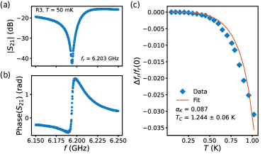
In order to accurately determine the inductance contribution of the tunable JJ, we must properly characterize the kinetic inductance of the superconductor thin film. For an Al thickness of 10 nm, we expect an appreciable kinetic inductance contribution to the total inductance of the resonator. We measure the kinetic inductance fraction of a bare CPW where is the measured frequency of the CPW Gao et al. (2006). Fig. 2(a) and (b) shows measurements of the phase and magnitude of complex transmission data of the resonant mode of R3. We find the measured resonant frequency to be while the frequency based on the geometry of the resonator is found to be , leading to a kinetic inductance fraction of . Considering the geometric inductance of R3, we find a kinetic inductance per square of . Using a two-fluid model to describe the contribution of kinetic inductance to the total inductance of the CPW Turneaure et al. (1991), we fit to the equation
| (1) |
where is the superconducting critical temperature and . For , we find that = 1.244 corresponding to a superconducting gap of 187 9 consistent with reported values for Al thin films Mayer et al. (2019); Dartiailh et al. (2021). We note that the kinetic inductance probes the superconducting condensate which also has a contribution from the InAs 2DEG along with the thin film Al Phan et al. (2022b).
IV Gate voltage tunability
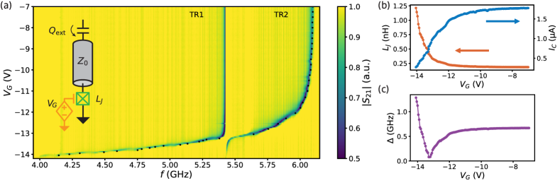
In order to achieve a wide tunability band, the junction must participate highly in the circuit. By galvanically connecting the junction to the CPW, we create an element that is continuously tuned in a wide dynamic range. In Fig. 3(a), we show versus while varying the gate voltage of TR2. The data taken here is at a power of -96 dBm. Two resonances are observed corresponding to the TR1 and TR2 modes at frequencies and , respectively. As tunes the occupation of the current carrying conduction channels in the JJ, there is a resulting decrease in the critical current , which is related to the Josephson inductance through where is the magnetic flux quantum. We find consequently that the TR2 mode is tuned to lower frequencies as the gate voltage decreases, showing a range of between V and , beyond which the resonant frequency drops outside of the measurement bandwidth of our setup.
Using calculated from R3, we can simulate the effect of the varying Josephson junction on the TR2 mode. By accounting for the effect of kinetic inductance in finite element simulations, we calculate the resonant frequency as a function of , which is represented by a lumped element inductor. Comparing these results to the measured frequencies, we obtain and as a function of shown in Fig. 3(b). We find that is highly tunable, increasing more than an order of magnitude between the highest and lowest points. One can define the Josephson inductive participation ratio in this circuit to be . Using the value of for TR2 and calculated by the kinetic inductance fraction, we find that at the lowest gate voltage measured , implying significant participation of the junction in the circuit. Previous studies based on InAs-Al nanowires have been restricted by either a limited tunability range or discrete switching of the coupler frequency Casparis et al. (2019); Splitthoff et al. (2022). The wide range and continuous tunability of this 2DEG-based device are advantageous for tunable coupling schemes.
Near we find that the two modes undergo an avoided level crossing. We define the difference in frequencies of the two modes as the detuning where and are the high and low frequency modes respectively. We show versus gate voltage in Fig. 3(c) and find that at applied, , while at strongest coupling, decreases to . At large negative gate values, then increases to at the lowest frequency of the TR2 mode. The on/off coupling ratio can then be determined as the detuning at the weakest coupling divided by the detuning at the strongest coupling. We find that the on/off coupling ratio at no applied gate voltage with is 8.47, and at large negative gate voltage with is 16.27. The latter value is limited by our measurement setup bandwidth and can be expected to increase further. We note that outside the strong coupling regime, the frequency of the TR1 mode remains unchanged due to the local effect of the TR2 gate, resulting in no detectable crosstalk.
V Josephson junction nonlinearity
One outstanding question in using voltage tunable junctions is whether the gate voltage control introduces power-dependent dissipation to the system along with the nonlinearity. This has previously been studied by embedding a JJ in a CPW and studying its high power response Boaknin et al. (2007). We employ a similar study as in Josephson tunnel junctions to understand the impact of gate voltage on the junction nonlinearity.
A combined CPW-JJ system can be described classically by a Duffing oscillator Landau and Lifshitz (1976); Manucharyan et al. (2007), where the nonlinearity gives rise to a power-dependent resonant frequency. At low input powers , the response has a familiar Lorentzian lineshape centered around the resonant frequency with a linewidth . As increases, the resonant frequency shifts to lower values, and at a critical power , the response becomes multivalued with two metastable solutions existing at a single frequency. This phenomenon is known as bifurcation and is the basis for Josephson bifurcation and parametric amplifiersYurke et al. (1989); Ho Eom et al. (2012); Siddiqi et al. (2004); Vijay et al. (2009); Phan et al. (2022a).
In order to keep track of the frequency at which bifurcation develops, we look at the susceptibility . We label the frequency at which the susceptibility is maximum . Assuming the low damping limit following Refs. Manucharyan et al. (2007) and Boaknin et al. (2007), one can rescale to the reduced frequency . In this way, we expect to be described by the curve
| (2) |
for powers and
| (3) |
for .
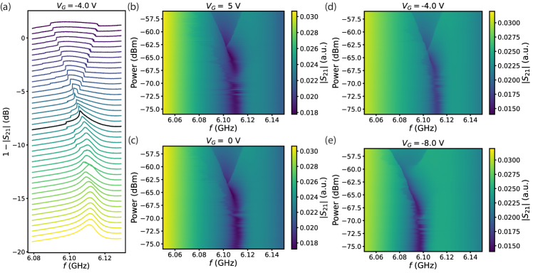
Fig. 4(a) shows the power-dependent response of the TR2 mode with a gate voltage applied to the gate electrode of TR2. We keep all other gates grounded. As the power increases, the resonant frequency shifts towards lower values, and when , an apparent discontinuity appears in the data. This is due to the hysteretic behavior of the bifurcation. Since we sweep the frequency in the positive direction, we probe only one solution branch at a time at powers greater than , and the apparent discontinuity corresponds to a jump from low to high amplitude solution branches. We find by identifying when the susceptibility first diverges. Further details on the procedure used to extract are described in the Supplementary Material and shown in Fig. S5. For , we find that ; the curve at this power is shown in black in Fig. 4(a). We note that the bifurcation of the TR2 mode is absent in the R3 mode. This implies that the nonlinearity in TR2 is mainly caused by the presence of the Josephson junction and not by the kinetic inductance of the thin Al film, as has been reported in other high kinetic inductance superconducting materials Niepce et al. (2019); Grünhaupt et al. (2018); Bretz-Sullivan et al. (2022).
We analyze the power-dependent response at different gate voltages shown in Fig. 4(b-e). We find that as the gate voltage is decreased, decreases as expected. Plotted in terms of the reduced frequency, in Fig. 5 we show versus at four different gate voltage values plotted with the theoretical curves predicted by Eqns. 2 and 3. To rescale to the reduced frequency , and are extracted from the fit of the resonance at . A summary of , and used to rescale the data are shown in the Supplementary Material Table S1.
We find that when plotted in terms of the reduced parameters, the data fall on the theoretical curve. Since the solutions to the Duffing model assume the low damping limit, agreement between the data and the theoretical prediction implies that the nonlinearity present in the superconductor-semiconductor junction is not caused by nonlinear dissipative effects. Furthermore, we find that this is true at all four gate voltages, reassuring the fact that applying a gate voltage introduces no additional power-dependent dissipation to the junction. Similar results showing the absence of power-dependent dissipation has been previously reported in AlO-Al junctions Boaknin et al. (2007), indicating that InAs-Al junctions have a similar nonlinearity. A discussion about microwave loss mechanisms and mitigation is provided in the Supplementary Material with measurements shown in Fig. S3. Deviations from the expected theoretical curve are most likely due to underestimating by taking it at a relatively high power compared to the critical powers here.
VI Avoided level crossing
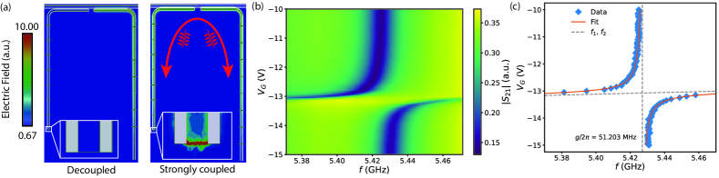
The wideband voltage tunability allows for coupling different resonators on the same chip. The coupling mechanism can be understood by studying the electric field distribution in the coupled and decoupled regimes, calculated using finite-element analysis methods. We find that in the decoupled scenario, two tunable resonator modes that are detuned by have an electric field squared at the frequency of one mode is distributed in the corresponding resonator as expected, shown in Fig. 6(a). This occurs when of the tunable resonator is set to . By tuning of the tunable resonator towards the frequency of the lower frequency mode, the two modes begin to hybridize, with the electric field energy now occupying both resonators. This corresponds to the strongly coupled regime, occurring when with a negative applied gate voltage.
The data presented in Fig. 6(b) shows such hybridization between TR2 and TR1 as TR2 is tuned to resulting in an avoided level crossing. By extracting the resonant frequencies of the two modes, we fit the data to a simple two-oscillator picture,
| (4) |
where is the coupling strength and , and are the uncoupled frequencies corresponding to the TR1 and TR2 modes, respectively. In this narrow gate voltage range, we assume the TR2 mode to have a frequency , which is approximately linear with the gate voltage changing at a rate of .628 .033 GHz/V. The TR1 mode is fixed at . Extracting the frequencies and from the data, we fit the two curves to obtain a coupling strength MHz as shown in Fig. 6(c). This value for taken from the fit to a two oscillators model is consistent with the conventional definition for being equal to half the minimum detuning, , which yields 51.765 MHz. We note that the coupling strength at this lower power is a bit larger than that which is found at higher power and shown in Fig. 3 of .
We hope to show that this device exhibits the basic necessary working principles to implement a tunable coupler using this architecture. The wideband tunablity of the InAs 2DEG device in particular demonstrates the advantage of using this over InAs nanowire based devices. In addition, the large coupling to another device on the same chip demonstrates a proof-of-principle experiment in which this tunable element can be used to couple different superconducting circuit elements on the same chip. We hope to use this device architecture for various applications which include as a tunable coupler between, say, two fixed frequency transmons or two gatemons. It has been shown that for coupler with 10 lifetime, a 50 CZ gate can be implemented with a gate fidelity of 99.5% Qi et al. (2018). An alternative use-case for this circuit is to implement a quantum memory which utilizes dynamically tunable couplers to access “storage cavities” which can store information. More details of such a device can be found in Ref. 43. We hope to have demonstrated in this report the ability to continuously tune the tunable resonator over a wide band, and in future experiments we would like to test dynamic tunability by sending high frequencies control signals through the gate voltage line.
VII Microwave loss measurements
A necessary consideration for the implementation of materials for superconducting qubit circuits is microwave loss. While semiconductor 2DEGs can offer wideband gate-tunable Josephson junctions (JJs), in this section we try to understand mechanisms which limit coherence in our devices.
| Device | Superconductor | Substrate | Gate |
|---|---|---|---|
| S1 - TR2 | 10 nm in-situ Al | 1 Buffer | Cr/Au |
| S1 - R3 | 10 nm in-situ Al | 1 Buffer | - |
| S2 | 100 nm sputtered Al | InP | - |
| S3 | 10 nm in-situ Al | 400 Buffer | - |
| S4 | 10 nm in-situ Al | 1 Buffer | Al |
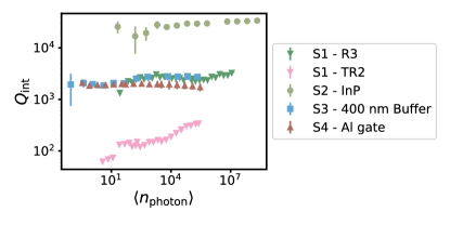
We fabricate and measure a series of CPW resonators and obtain internal quality factors for each sample. These samples aim to study loss mechanisms introduced by specific device conditions. These include loss due to the substrate, the epitaxial III-V layers, the thin film superconductor, and the gate electrode. Details of the devices are discussed in Table 2 and further information can be found in the Supplementary Material.
We show a summary of these measurements in Fig. 7 where we present power dependence of for all samples. We find an internal quality factor for the CPW on InP to be at an average photon number of . This is consistent with other reports of for CPW resonators on InP substrates Casparis et al. (2018) and piezoelectricity has commonly been attributed as the dominant loss mechanism Scigliuzzo et al. (2020); McRae et al. (2021). By growing the III-V heterostructure on Si, it should be possible to increase the upper bound on for these circuits to more than McRae et al. (2020). Alternatively, one can use a flip-chip device design, to concentrate the energy participation in a low loss probe wafer Hazard et al. (2022).
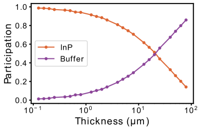
We compare the results for CPWs on the InP substrate to the bare resonator device, R3 on sample S1. We find that at low power, . To understand the source of this added loss, we also measure a sample with a 400 nm epitaxial III-V layer, S3. We find that is almost identical to that of R3 in sample S1 which has a 1 epitaxial III-V layer. By accounting for differences in energy participation of the buffer layers for the and buffers, being 3.5% and 7.0% respectively. Details of the participation ratio calculations can be found in the Supplementary Material. Despite the increased epitaxial III-V layer participation, we find that in our devices the epitaxial III-V layers do not significantly affect . Thus, we believe this decrease in is due to the thin film Al. This has previously been observed in other high kinetic inductance materials, such as NbTiN thin films and nanowires Peltonen et al. (2016, 2018); Bretz-Sullivan et al. (2022).
We next consider loss due to the gate electrode. While the large participation of the Josephson junction in the circuit provides considerable frequency tunability, the electric field across the junction may couple to the gate electrode. We find that in sample S1, at low power, the TR2 mode has an order of magnitude lower than that of R3 on the same chip. We compare this to sample S2 which has a tunable resonator which replaces the Cr/Au gate with Al. We find that of this device is at low power, approaching that of S1 - R3 and S3. This suggests that TR2 has coherence limited by the Cr/Au gate electrode. In addition to the findings raised hee, promising new directions in reducing losses in these materials are using hexagonal boron nitride (h-BN) as a gate dielectric, Barati et al. (2021); Wang et al. (2022). This discussion hopefully provides a path forward for increasing of tunable resonators on InAs 2DEGs.
VIII Conclusion
In conclusion, we have demonstrated the wideband tunability of a superconductor-semiconductor based tunable resonator. We show that the gate voltage tunable junction has a non-dissipative nonlinearity, ideal for implementing in superconducting qubit circuits. After adjusting for the kinetic inductance of the Al thin film, we find that the Josephson inductance is tunable by up to an order of magnitude, achieving a high participation in the circuit of 44. This high participation enables us to continuously tune the resonant frequency of the tunable resonator mode by more than 2 GHz. We also show that by tuning the tunable resonator mode into resonance with another resonator on the chip, we observe hybridization of the two modes through an avoided level crossing, with coupling strength of . The wide tunability range results in large detuning of the two modes resulting in an on/off detuning ratio of 16 at large negative gate voltage and 8 at applied. While is quite low, we find that the coherence is limited by the normal metal gate line and discuss tangible improvements which can be made to material and device design which can significantly enhance of InAs 2DEG tunable resonators. The ability to achieve strong coupling and large detuning between the two modes makes this device design an ideal platform for qubit-qubit coupling schemes and quantum information storage where the TR mode, acting as a coupler, can be brought into resonance with a fixed frequency mode by dynamically pulsing the gate.
IX Acknowledgements
We thank Patrick J. Strohbeen, Matthieu Dartiailh, Jaewoo Lee, and Nicholas Materise for fruitful discussions. The authors acknowledge support from the Army Research Office agreement W911NF2110303. The N.Y.U. team acknowledges support from the Army Research Office agreement W911NF2210048 and from the National Science Foundation agreement 2340-206-2014878 A01. W.M.S. acknowledges funding from the ARO/LPS QuaCR Graduate Fellowship. W.F.S. acknowledges funding from the NDSEG Fellowship. This work was performed in part at the Nanofabrication Facility at the Advanced Science Research Center at The Graduate Center of the City University of New York.
X Appendix A: Materials growth
The devices studied are fabricated on a heterostructure grown by molecular beam epitaxy. On an epi-ready, semi-insulating thick InP (100) substrate, a thick In0.52Al0.48As/In0.53Ga0.47As superlattice of ten periods is grown followed by a 50 nm thick In0.52Al0.48As layer and an thick InxAl1-xAs graded buffer layer in which the composition is step graded between and in steps of . This is followed by a In0.81Al0.19As virtual substrate. The structure is then modulation doped with Si at a density of . Following a 6 nm In0.81Al0.19As spacer, an InAs near-surface quantum well is then grown between two layers of In0.81Ga0.19As, where the top barrier layer is thick and the bottom barrier layer is thick. The structure is then capped with a 10 nm layer of Al grown in-situ. Further details on the materials growth procedure are provided in Refs. Shabani et al. (2016); Wickramasinghe et al. (2018); Yuan et al. (2020); Strickland et al. (2022). Through low temperature magnetotransport measurements, we find the wafer used in this device has a 2D electron density of and an electron mobility of measured along the crystal direction. This corresponds to an electron mean free path of . With the Josephson junction weak-link being long, the junction is expected to be in the short ballistic regime Mayer et al. (2019).
XI Appendix B: Design and fabrication
The design was constructed using Qiskit Metal Minev et al. (2021) and rendered in Ansys’s high frequency simulation software (HFSS) ans to simulate for the expected resonant frequency, external quality factors and electromagnetic field distribution. We use electron beam lithography to define patterns in spin-coated polymethylmethacrylate (PMMA) resist. To define the microwave circuit, Al is removed with Transene Al etchant type-D followed by a wet etch down to the buffer layer using a III-V etchant consisting of phosphoric acid (H3PO4, 85%), hydrogen peroxide (H2O2, 30%) and deionized water in a volumetric ratio of 1:1:40. To define the Josephson junctions, we etch away a long, wide strip of aluminum from the CPW mesa. We then deposit of AlO to serve as a gate dielectric by atomic layer deposition at . This is followed by another electron beam lithography patterning step to define the gate pattern and an electron beam deposition of the gate electrode, consisting of Cr and of Au. An optical image of the fabricated and wirebonded chip is shown in Fig. 8.
A series of samples are used to fabricate CPW devices for measurements. The first is a CPW with 100 nm Al deposited on an InP substrate. The second is a 400 nm thick III-V heterostructure grown by MBE with a thin in-situ deposited Al film. The last is a CPW on hte same wafer as that which is reported here, but with superconducting Al as the gate electrode as opposed to a combination of Cr and Au. The 400 buffer resonator was fabricated on the thin in-situ aluminum on a similar layer structure as mentioned in this report, but with graded buffer layer steps of rather than , giving rise to a total thickness of approximately 400 nm. The Al growth conditions are nominally identical to that of the wafer presented previously. The InP wafer has 100 nm aluminum sputtered by DC magnetron sputtering after an Ar plasma cleaning in order to etch the native oxide. The design consists of a common feedline with hanger CPW resonators with the same central conductor width and spacing to the ground plane as the device in the main text. The simulated for each CPW is 7830. The measured resonant frequency of the InP resonator is and that of the 400 nm buffer resonator is .
XII Appendix C: Measurement setup
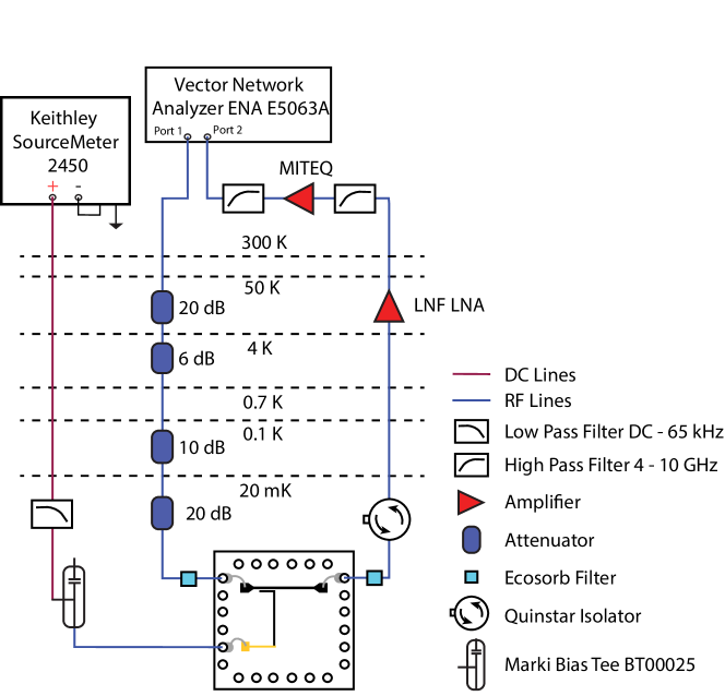
A schematic of the measurement setup is shown in Fig. 9. Measurements are conducted in an Oxford Triton dilution refrigerator. The sample is embedded in a QCage, a microwave sample holder manufactured by QDevil, and connected to the printed circuit board by aluminum wirebonds. Probe signals are sent from a vector network analyzer (Port 1) attenuated by -56 dBm with attenuation at each plate as noted. Attenuators are made by XMA. The signal then passes through a 1-18 GHz bandpass filter made by a copper box filled with cured Eccosorb castable epoxy resin. The signal is sent through the sample and returned through another Eccosorb filter, passed through an isolator with 20 dB isolation and 0.2 dB insertion loss, and then amplified with a low noise amplifier mounted to the 4K plate, as well as a room temperature amplifier (MITEQ) at room temperature. The gate electrode is connected to a voltage source and passed through a QFilter, a low pass filter manufactured by QDevil, mounted at the mixing chamber plate.
XIII Appendix D: Tunable resonator design
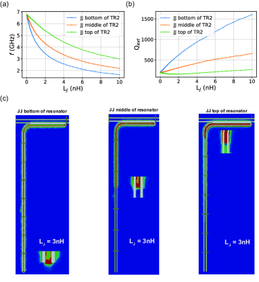
The details of the tunability the junction provides depends heavily on aspects of the design. The device presented in the manuscript has the JJ at the bottom of the resonator, directly shorting it to ground. Here, we also consider two other cases where the junction is in the middle and at the top of the resonator. As seen in Fig. 10, having the junction at the bottom of the resonator provides slightly more tunability in while enhancing the value of compared to the two other cases. On the other hand, having the junction at the top (right before the bend) of the resonator provides slightly less tunability in while barely changing . The range tunability of can be modified further by changing the initial value of and by switching the open and grounded ends of the CPW.
Fig. 10c presents the electric field profile of TR2 for the three cases with L . The distribution and concentration of the field can be seen to vary with the position of the junction. With the junction at the top of the resonator, the field can be seen to be restricted to the top part of the resonator while the rest of the resonator is isolated. This kind of isolation is ideal for superconducting quantum memory Sardashti et al. (2020).
XIV Appendix E: Critical power extraction
| () | () | () | |
|---|---|---|---|
| 5 | 6.114 | 4355 | -64.3 |
| 0 | 6.114 | 4732 | -64.5 |
| -4 | 6.113 | 5362 | -65.6 |
| -8 | 6.100 | 4971 | -64.7 |
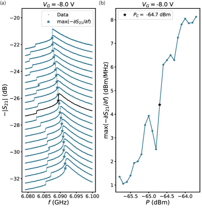
In the bifurcation analysis, we find the critical power by analyzing the signal which is a function of frequency and input power . By discrete differentiation with respect to for fixed , we get . The data is sampled with 1201 points in a span of . The frequency at which the curve exhibits the highest derivative is defined as and the value of the derivative at this point is which depends on the power .
As increases, the critical point can be identified when first diverges. This divergence is due to the nature of the multi-valued solution of the Duffing equation which governs the systems behavior. When sweeping the frequency forward (from negative to positive), we find that the VNA probes only one solution branch at a time at powers greater than . This gives rise to an apparent discontinuity in the data as seen in Fig. 11a. We note that both solutions can be observed if one were to probe the system by sweeping frequency in the backward direction.
In order to identify the critical point, we look for the point at which the as a function of first . By taking a second derivative with respect to , we identify at which power a sharp increase by finding the maximum,
The critical power is the power at which this occurs. Here, . An example of such extraction for is presented in Fig. 11 and we summarize the various extracted for different gate voltages shown in Table 3. We also include the frequencies and loaded quality factor used to rescale for Fig. 11.
XV Appendix F: Participation ratio calculations
We further understand the buffer layer contributions to the loss by calculating the participation of the buffer layer and substrate as a function of buffer layer thickness using finite-element analysis (HFSS ans ). The participation ratio is the ratio of the total electric field squared integrated over each volume
Here only takes into account the InP substrate and the buffer layer. Fig. 12 shows of the buffer layer and InP as a function of the thickness of the buffer layer. The participation ratio of the buffer layer is seen to increase with the thickness of the buffer laye which is expected.
References
- Kjaergaard et al. (2020) M. Kjaergaard, M. E. Schwartz, J. Braumüller, P. Krantz, J. I.-J. Wang, S. Gustavsson, and W. D. Oliver, Annual Review of Condensed Matter Physics 11, 369 (2020), eprint https://doi.org/10.1146/annurev-conmatphys-031119-050605, URL https://doi.org/10.1146/annurev-conmatphys-031119-050605.
- Blais et al. (2021) A. Blais, A. L. Grimsmo, S. M. Girvin, and A. Wallraff, Rev. Mod. Phys. 93, 025005 (2021), URL https://link.aps.org/doi/10.1103/RevModPhys.93.025005.
- Wallraff et al. (2004) A. Wallraff, D. I. Schuster, A. Blais, L. Frunzio, R.-S. Huang, J. Majer, S. Kumar, S. M. Girvin, and R. J. Schoelkopf, Nature 431, 162 (2004), ISSN 1476-4687, URL https://doi.org/10.1038/nature02851.
- Blais et al. (2004) A. Blais, R.-S. Huang, A. Wallraff, S. M. Girvin, and R. J. Schoelkopf, Phys. Rev. A 69, 062320 (2004), URL https://link.aps.org/doi/10.1103/PhysRevA.69.062320.
- Koch et al. (2007) J. Koch, T. M. Yu, J. Gambetta, A. A. Houck, D. I. Schuster, J. Majer, A. Blais, M. H. Devoret, S. M. Girvin, and R. J. Schoelkopf, Phys. Rev. A 76, 042319 (2007), URL https://link.aps.org/doi/10.1103/PhysRevA.76.042319.
- Gyenis et al. (2021) A. Gyenis, A. Di Paolo, J. Koch, A. Blais, A. A. Houck, and D. I. Schuster, PRX Quantum 2, 030101 (2021), URL https://link.aps.org/doi/10.1103/PRXQuantum.2.030101.
- Place et al. (2020) A. P. M. Place, L. V. H. Rodgers, P. Mundada, B. M. Smitham, M. Fitzpatrick, Z. Leng, A. Premkumar, J. Bryon, S. Sussman, G. Cheng, et al. (2020), eprint 2003.00024.
- Somoroff et al. (2021) A. Somoroff, Q. Ficheux, R. A. Mencia, H. Xiong, R. V. Kuzmin, and V. E. Manucharyan, Millisecond coherence in a superconducting qubit (2021), URL https://arxiv.org/abs/2103.08578.
- McKay et al. (2019) D. C. McKay, S. Sheldon, J. A. Smolin, J. M. Chow, and J. M. Gambetta, Phys. Rev. Lett. 122, 200502 (2019), URL https://link.aps.org/doi/10.1103/PhysRevLett.122.200502.
- Yan et al. (2018) F. Yan, P. Krantz, Y. Sung, M. Kjaergaard, D. L. Campbell, T. P. Orlando, S. Gustavsson, and W. D. Oliver, Phys. Rev. Applied 10, 054062 (2018), URL https://link.aps.org/doi/10.1103/PhysRevApplied.10.054062.
- Mundada et al. (2019) P. Mundada, G. Zhang, T. Hazard, and A. Houck, Phys. Rev. Applied 12, 054023 (2019), URL https://link.aps.org/doi/10.1103/PhysRevApplied.12.054023.
- Sung et al. (2021) Y. Sung, L. Ding, J. Braumüller, A. Vepsäläinen, B. Kannan, M. Kjaergaard, A. Greene, G. O. Samach, C. McNally, D. Kim, et al., Phys. Rev. X 11, 021058 (2021), URL https://link.aps.org/doi/10.1103/PhysRevX.11.021058.
- Foxen et al. (2020) B. Foxen, C. Neill, A. Dunsworth, P. Roushan, B. Chiaro, A. Megrant, J. Kelly, Z. Chen, K. Satzinger, R. Barends, et al. (Google AI Quantum), Phys. Rev. Lett. 125, 120504 (2020), URL https://link.aps.org/doi/10.1103/PhysRevLett.125.120504.
- Chen et al. (2014) Y. Chen, C. Neill, P. Roushan, N. Leung, M. Fang, R. Barends, J. Kelly, B. Campbell, Z. Chen, B. Chiaro, et al., Phys. Rev. Lett. 113, 220502 (2014), URL https://link.aps.org/doi/10.1103/PhysRevLett.113.220502.
- Sheldon et al. (2016) S. Sheldon, E. Magesan, J. M. Chow, and J. M. Gambetta, Phys. Rev. A 93, 060302 (2016), URL https://link.aps.org/doi/10.1103/PhysRevA.93.060302.
- Kandala et al. (2021) A. Kandala, K. X. Wei, S. Srinivasan, E. Magesan, S. Carnevale, G. A. Keefe, D. Klaus, O. Dial, and D. C. McKay, Phys. Rev. Lett. 127, 130501 (2021), URL https://link.aps.org/doi/10.1103/PhysRevLett.127.130501.
- Orlando et al. (1999) T. P. Orlando, J. E. Mooij, L. Tian, C. H. van der Wal, L. S. Levitov, S. Lloyd, and J. J. Mazo, Phys. Rev. B 60, 15398 (1999), URL https://link.aps.org/doi/10.1103/PhysRevB.60.15398.
- Chiorescu et al. (2003) I. Chiorescu, Y. Nakamura, C. J. P. M. Harmans, and J. E. Mooij, Science 299, 1869 (2003), eprint https://www.science.org/doi/pdf/10.1126/science.1081045, URL https://www.science.org/doi/abs/10.1126/science.1081045.
- Palacios-Laloy et al. (2008) A. Palacios-Laloy, F. Nguyen, F. Mallet, P. Bertet, D. Vion, and D. Esteve, Journal of Low Temperature Physics 151, 1034 (2008), ISSN 0022-2291, 1573-7357, URL http://link.springer.com/10.1007/s10909-008-9774-x.
- Naaman et al. (2016) O. Naaman, M. O. Abutaleb, C. Kirby, and M. Rennie, Applied Physics Letters 108, 112601 (2016), ISSN 0003-6951, 1077-3118, URL http://aip.scitation.org/doi/10.1063/1.4943602.
- Kakuyanagi et al. (2007) K. Kakuyanagi, T. Meno, S. Saito, H. Nakano, K. Semba, H. Takayanagi, F. Deppe, and A. Shnirman, Phys. Rev. Lett. 98, 047004 (2007), URL https://link.aps.org/doi/10.1103/PhysRevLett.98.047004.
- Hutchings et al. (2017) M. Hutchings, J. Hertzberg, Y. Liu, N. Bronn, G. Keefe, M. Brink, J. M. Chow, and B. Plourde, Physical Review Applied 8, 044003 (2017), ISSN 2331-7019, URL https://link.aps.org/doi/10.1103/PhysRevApplied.8.044003.
- Kumar et al. (2016) P. Kumar, S. Sendelbach, M. A. Beck, J. W. Freeland, Z. Wang, H. Wang, C. C. Yu, R. Q. Wu, D. P. Pappas, and R. McDermott, Phys. Rev. Applied 6, 041001 (2016), URL https://link.aps.org/doi/10.1103/PhysRevApplied.6.041001.
- Bialczak et al. (2007) R. C. Bialczak, R. McDermott, M. Ansmann, M. Hofheinz, N. Katz, E. Lucero, M. Neeley, A. D. O’Connell, H. Wang, A. N. Cleland, et al., Phys. Rev. Lett. 99, 187006 (2007), URL https://link.aps.org/doi/10.1103/PhysRevLett.99.187006.
- Beenakker (1992) C. W. J. Beenakker, Phys. Rev. B 46, 12841 (1992), URL https://link.aps.org/doi/10.1103/PhysRevB.46.12841.
- Mayer et al. (2019) W. Mayer, J. Yuan, K. S. Wickramasinghe, T. Nguyen, M. C. Dartiailh, and J. Shabani, Applied Physics Letters 114, 103104 (2019).
- Nichele et al. (2017) F. Nichele, A. C. C. Drachmann, A. M. Whiticar, E. C. T. O’Farrell, H. J. Suominen, A. Fornieri, T. Wang, G. C. Gardner, C. Thomas, A. T. Hatke, et al., Phys. Rev. Lett. 119, 136803 (2017).
- Suominen et al. (2017) H. J. Suominen, M. Kjaergaard, A. R. Hamilton, J. Shabani, C. J. Palmstrøm, C. M. Marcus, and F. Nichele, Phys. Rev. Lett. 119, 176805 (2017).
- Kjaergaard et al. (2017) M. Kjaergaard, H. J. Suominen, M. P. Nowak, A. R. Akhmerov, J. Shabani, C. J. Palmstrøm, F. Nichele, and C. M. Marcus, Phys. Rev. Applied 7, 034029 (2017).
- Elfeky et al. (2021) B. H. Elfeky, N. Lotfizadeh, W. F. Schiela, W. M. Strickland, M. Dartiailh, K. Sardashti, M. Hatefipour, P. Yu, N. Pankratova, H. Lee, et al., Nano Letters 21, 8274 (2021), ISSN 1530-6984, publisher: American Chemical Society, URL https://doi.org/10.1021/acs.nanolett.1c02771.
- de Lange et al. (2015) G. de Lange, B. van Heck, A. Bruno, D. J. van Woerkom, A. Geresdi, S. R. Plissard, E. P. A. M. Bakkers, A. R. Akhmerov, and L. DiCarlo, Phys. Rev. Lett. 115, 127002 (2015), URL https://link.aps.org/doi/10.1103/PhysRevLett.115.127002.
- Larsen et al. (2015) T. W. Larsen, K. D. Petersson, F. Kuemmeth, T. S. Jespersen, P. Krogstrup, J. Nygård, and C. M. Marcus, Phys. Rev. Lett. 115, 127001 (2015), URL https://link.aps.org/doi/10.1103/PhysRevLett.115.127001.
- Luthi et al. (2018) F. Luthi, T. Stavenga, O. W. Enzing, A. Bruno, C. Dickel, N. K. Langford, M. A. Rol, T. S. Jespersen, J. Nygård, P. Krogstrup, et al., Phys. Rev. Lett. 120, 100502 (2018), URL https://link.aps.org/doi/10.1103/PhysRevLett.120.100502.
- Kringhøj et al. (2018) A. Kringhøj, L. Casparis, M. Hell, T. W. Larsen, F. Kuemmeth, M. Leijnse, K. Flensberg, P. Krogstrup, J. Nygård, K. D. Petersson, et al., Phys. Rev. B 97, 060508 (2018).
- Casparis et al. (2018) L. Casparis, M. R. Connolly, M. Kjaergaard, N. J. Pearson, A. Kringhøj, T. W. Larsen, F. Kuemmeth, T. Wang, C. Thomas, S. Gronin, et al., Nature Nanotechnology 13, 915 (2018).
- Casparis et al. (2016) L. Casparis, T. W. Larsen, M. S. Olsen, F. Kuemmeth, P. Krogstrup, J. Nygård, K. D. Petersson, and C. M. Marcus, Phys. Rev. Lett. 116, 150505 (2016), URL https://link.aps.org/doi/10.1103/PhysRevLett.116.150505.
- O’Connell Yuan et al. (2021) J. O’Connell Yuan, K. S. Wickramasinghe, W. M. Strickland, M. C. Dartiailh, K. Sardashti, M. Hatefipour, and J. Shabani, Journal of Vacuum Science & Technology A 39, 033407 (2021).
- Larsen et al. (2020) T. W. Larsen, M. E. Gershenson, L. Casparis, A. Kringhøj, N. J. Pearson, R. P. G. McNeil, F. Kuemmeth, P. Krogstrup, K. D. Petersson, and C. M. Marcus, Phys. Rev. Lett. 125, 056801 (2020), URL https://link.aps.org/doi/10.1103/PhysRevLett.125.056801.
- Danilenko et al. (2022) A. Danilenko, D. Sabonis, G. W. Winkler, O. Erlandsson, P. Krogstrup, and C. M. Marcus, Few-mode to mesoscopic junctions in gatemon qubits (2022), URL https://arxiv.org/abs/2209.03688.
- Hertel et al. (2022) A. Hertel, M. Eichinger, L. O. Andersen, D. M. T. van Zanten, S. Kallatt, P. Scarlino, A. Kringhøj, J. M. Chavez-Garcia, G. C. Gardner, S. Gronin, et al., Gate-tunable transmon using selective-area-grown superconductor-semiconductor hybrid structures on silicon (2022), URL https://arxiv.org/abs/2202.10860.
- Casparis et al. (2019) L. Casparis, N. J. Pearson, A. Kringhøj, T. W. Larsen, F. Kuemmeth, J. Nygård, P. Krogstrup, K. D. Petersson, and C. M. Marcus, Phys. Rev. B 99, 085434 (2019), URL https://link.aps.org/doi/10.1103/PhysRevB.99.085434.
- Qi et al. (2018) Z. Qi, H. Xie, J. Shabani, V. E. Manucharyan, A. Levchenko, and M. G. Vavilov, Phys. Rev. B 97, 134518 (2018).
- Sardashti et al. (2020) K. Sardashti, M. C. Dartiailh, J. Yuan, S. Hart, P. Gumann, and J. Shabani, IEEE Transactions on Quantum Engineering 1, 1 (2020).
- Phan et al. (2022a) D. Phan, P. Falthansl-Scheinecker, U. Mishra, W. M. Strickland, D. Langone, J. Shabani, and A. P. Higginbotham, Semiconductor quantum-limited amplifier (2022a), URL https://arxiv.org/abs/2206.05746.
- Scarlino et al. (2019) P. Scarlino, D. J. van Woerkom, U. C. Mendes, J. V. Koski, A. J. Landig, C. K. Andersen, S. Gasparinetti, C. Reichl, W. Wegscheider, K. Ensslin, et al., Nature Communications 10, 3011 (2019), ISSN 2041-1723, URL https://doi.org/10.1038/s41467-019-10798-6.
- Borjans et al. (2020) F. Borjans, X. G. Croot, X. Mi, M. J. Gullans, and J. R. Petta, Nature 577, 195 (2020), ISSN 1476-4687, URL https://doi.org/10.1038/s41586-019-1867-y.
- Burkard et al. (2020) G. Burkard, M. J. Gullans, X. Mi, and J. R. Petta, Nature Reviews Physics 2, 129 (2020), ISSN 2522-5820, URL https://doi.org/10.1038/s42254-019-0135-2.
- Hays et al. (2020) M. Hays, V. Fatemi, K. Serniak, D. Bouman, S. Diamond, G. de Lange, P. Krogstrup, J. Nygård, A. Geresdi, and M. H. Devoret, Nature Physics 16, 1103 (2020), ISSN 1745-2481.
- Hays et al. (2021) M. Hays, V. Fatemi, D. Bouman, J. Cerrillo, S. Diamond, K. Serniak, T. Connolly, P. Krogstrup, J. Nygård, A. L. Yeyati, et al., Science 373, 430 (2021).
- Leroux et al. (2022) C. Leroux, A. Parra-Rodriguez, R. Shillito, A. Di Paolo, W. D. Oliver, C. M. Marcus, M. Kjaergaard, A. Gyenis, and A. Blais, Nonreciprocal devices based on voltage-tunable junctions (2022), URL https://arxiv.org/abs/2209.06194.
- Shabani et al. (2016) J. Shabani, M. Kjaergaard, H. J. Suominen, Y. Kim, F. Nichele, K. Pakrouski, T. Stankevic, R. M. Lutchyn, P. Krogstrup, R. Feidenhans’l, et al., Phys. Rev. B 93, 155402 (2016).
- Wickramasinghe et al. (2018) K. S. Wickramasinghe, W. Mayer, J. Yuan, T. Nguyen, L. Jiao, V. Manucharyan, and J. Shabani, Applied Physics Letters 113, 262104 (2018).
- Yuan et al. (2020) J. Yuan, M. Hatefipour, B. A. Magill, W. Mayer, M. C. Dartiailh, K. Sardashti, K. S. Wickramasinghe, G. A. Khodaparast, Y. H. Matsuda, Y. Kohama, et al., Phys. Rev. B 101, 205310 (2020).
- Strickland et al. (2022) W. M. Strickland, M. Hatefipour, D. Langone, S. M. Farzaneh, and J. Shabani, Applied Physics Letters 121, 092104 (2022), eprint https://doi.org/10.1063/5.0101579, URL https://doi.org/10.1063/5.0101579.
- Probst et al. (2015) S. Probst, F. B. Song, P. A. Bushev, A. V. Ustinov, and M. Weides, Review of Scientific Instruments 86, 024706 (2015), eprint https://doi.org/10.1063/1.4907935, URL https://doi.org/10.1063/1.4907935.
- Minev et al. (2021) Z. K. Minev, T. G. McConkey, J. Drysdale, P. Shah, D. Wang, M. Facchini, G. Harper, J. Blair, H. Zhang, N. Lanzillo, et al., Qiskit Metal: An Open-Source Framework for Quantum Device Design & Analysis (2021), URL https://doi.org/10.5281/zenodo.4618153.
- Simons (2001) R. N. Simons, Conventional Coplanar Waveguide (John Wiley Sons, Ltd, 2001), chap. 2, pp. 11–86, ISBN 9780471224754.
- Pozar (2012) D. M. Pozar, Microwave engineering (Fourth edition. Hoboken, NJ : Wiley, 2012 ©2012, 2012).
- Göppl et al. (2008) M. Göppl, A. Fragner, M. Baur, R. Bianchetti, S. Filipp, J. M. Fink, P. J. Leek, G. Puebla, L. Steffen, and A. Wallraff, Journal of Applied Physics 104, 113904 (2008), eprint https://doi.org/10.1063/1.3010859, URL https://doi.org/10.1063/1.3010859.
- (60) ANSYS HFSS Software: http://www.ansoft.com/products/hf/hfss/.
- Gao et al. (2006) J. Gao, J. Zmuidzinas, B. Mazin, P. Day, and H. Leduc, Nuclear Instruments and Methods in Physics Research Section A: Accelerators, Spectrometers, Detectors and Associated Equipment 559, 585 (2006), ISSN 0168-9002, proceedings of the 11th International Workshop on Low Temperature Detectors, URL https://www.sciencedirect.com/science/article/pii/S0168900205025003.
- Turneaure et al. (1991) J. P. Turneaure, J. Halbritter, and H. A. Schwettman, Journal of Superconductivity 4, 341 (1991), ISSN 1572-9605, URL https://doi.org/10.1007/BF00618215.
- Dartiailh et al. (2021) M. C. Dartiailh, W. Mayer, J. Yuan, K. S. Wickramasinghe, A. Matos-Abiague, I. Žutić, and J. Shabani, Phys. Rev. Lett. 126, 036802 (2021), URL https://link.aps.org/doi/10.1103/PhysRevLett.126.036802.
- Phan et al. (2022b) D. Phan, J. Senior, A. Ghazaryan, M. Hatefipour, W. M. Strickland, J. Shabani, M. Serbyn, and A. P. Higginbotham, Phys. Rev. Lett. 128, 107701 (2022b), URL https://link.aps.org/doi/10.1103/PhysRevLett.128.107701.
- Splitthoff et al. (2022) L. J. Splitthoff, A. Bargerbos, L. Grünhaupt, M. Pita-Vidal, J. J. Wesdorp, Y. Liu, A. Kou, C. K. Andersen, and B. van Heck, Gate-tunable kinetic inductance in proximitized nanowires (2022), URL https://arxiv.org/abs/2202.08729.
- Boaknin et al. (2007) E. Boaknin, V. E. Manucharyan, S. Fissette, M. Metcalfe, L. Frunzio, R. Vijay, I. Siddiqi, A. Wallraff, R. J. Schoelkopf, and M. Devoret, Dispersive microwave bifurcation of a superconducting resonator cavity incorporating a josephson junction (2007), URL https://arxiv.org/abs/cond-mat/0702445.
- Landau and Lifshitz (1976) L. D. Landau and E. M. Lifshitz, Mechanics, Third Edition: Volume 1 (Course of Theoretical Physics) (Butterworth-Heinemann, 1976), 3rd ed., ISBN 0750628960, URL http://www.worldcat.org/isbn/0750628960.
- Manucharyan et al. (2007) V. E. Manucharyan, E. Boaknin, M. Metcalfe, R. Vijay, I. Siddiqi, and M. Devoret, Phys. Rev. B 76, 014524 (2007), URL https://link.aps.org/doi/10.1103/PhysRevB.76.014524.
- Yurke et al. (1989) B. Yurke, L. R. Corruccini, P. G. Kaminsky, L. W. Rupp, A. D. Smith, A. H. Silver, R. W. Simon, and E. A. Whittaker, Phys. Rev. A 39, 2519 (1989), URL https://link.aps.org/doi/10.1103/PhysRevA.39.2519.
- Ho Eom et al. (2012) B. Ho Eom, P. K. Day, H. G. LeDuc, and J. Zmuidzinas, Nature Physics 8, 623 (2012), ISSN 1745-2481, URL https://doi.org/10.1038/nphys2356.
- Siddiqi et al. (2004) I. Siddiqi, R. Vijay, F. Pierre, C. M. Wilson, M. Metcalfe, C. Rigetti, L. Frunzio, and M. H. Devoret, Phys. Rev. Lett. 93, 207002 (2004), URL https://link.aps.org/doi/10.1103/PhysRevLett.93.207002.
- Vijay et al. (2009) R. Vijay, M. H. Devoret, and I. Siddiqi, Review of Scientific Instruments 80, 111101 (2009), eprint https://doi.org/10.1063/1.3224703, URL https://doi.org/10.1063/1.3224703.
- Niepce et al. (2019) D. Niepce, J. Burnett, and J. Bylander, Phys. Rev. Applied 11, 044014 (2019), URL https://link.aps.org/doi/10.1103/PhysRevApplied.11.044014.
- Grünhaupt et al. (2018) L. Grünhaupt, N. Maleeva, S. T. Skacel, M. Calvo, F. Levy-Bertrand, A. V. Ustinov, H. Rotzinger, A. Monfardini, G. Catelani, and I. M. Pop, Phys. Rev. Lett. 121, 117001 (2018), URL https://link.aps.org/doi/10.1103/PhysRevLett.121.117001.
- Bretz-Sullivan et al. (2022) T. M. Bretz-Sullivan, R. M. Lewis, A. L. Lima-Sharma, D. Lidsky, C. M. Smyth, C. T. Harris, M. Venuti, S. Eley, and T.-M. Lu, Applied Physics Letters 121, 052602 (2022), eprint https://doi.org/10.1063/5.0100961, URL https://doi.org/10.1063/5.0100961.
- Scigliuzzo et al. (2020) M. Scigliuzzo, L. E. Bruhat, A. Bengtsson, J. J. Burnett, A. F. Roudsari, and P. Delsing, New Journal of Physics 22, 053027 (2020), URL https://doi.org/10.1088/1367-2630/ab8044.
- McRae et al. (2021) C. R. H. McRae, A. McFadden, R. Zhao, H. Wang, J. L. Long, T. Zhao, S. Park, M. Bal, C. J. Palmstrøm, and D. P. Pappas, Journal of Applied Physics 129, 025109 (2021), eprint https://doi.org/10.1063/5.0029855, URL https://doi.org/10.1063/5.0029855.
- McRae et al. (2020) C. R. H. McRae, H. Wang, J. Gao, M. R. Vissers, T. Brecht, A. Dunsworth, D. P. Pappas, and J. Mutus, Review of Scientific Instruments 91, 091101 (2020), eprint https://doi.org/10.1063/5.0017378, URL https://doi.org/10.1063/5.0017378.
- Hazard et al. (2022) T. M. Hazard, A. J. Kerman, K. Serniak, and C. Tahan, Superconducting-semiconducting voltage-tunable qubits in the third dimension (2022), URL https://arxiv.org/abs/2203.06209.
- Peltonen et al. (2016) J. T. Peltonen, Z. H. Peng, Y. P. Korneeva, B. M. Voronov, A. A. Korneev, A. V. Semenov, G. N. Gol’tsman, J. S. Tsai, and O. V. Astafiev, Phys. Rev. B 94, 180508 (2016), URL https://link.aps.org/doi/10.1103/PhysRevB.94.180508.
- Peltonen et al. (2018) J. T. Peltonen, P. C. J. J. Coumou, Z. H. Peng, T. M. Klapwijk, J. S. Tsai, and O. V. Astafiev, Scientific Reports 8, 10033 (2018), ISSN 2045-2322, URL https://doi.org/10.1038/s41598-018-27154-1.
- Barati et al. (2021) F. Barati, J. P. Thompson, M. C. Dartiailh, K. Sardashti, W. Mayer, J. Yuan, K. Wickramasinghe, K. Watanabe, T. Taniguchi, H. Churchill, et al., Nano Letters 21, 1915 (2021), ISSN 1530-6984, URL https://doi.org/10.1021/acs.nanolett.0c03183.
- Wang et al. (2022) J. I.-J. Wang, M. A. Yamoah, Q. Li, A. H. Karamlou, T. Dinh, B. Kannan, J. Braumüller, D. Kim, A. J. Melville, S. E. Muschinske, et al., Nature Materials 21, 398 (2022), ISSN 1476-4660, URL https://doi.org/10.1038/s41563-021-01187-w.