Integrated Buried Heaters for Efficient Spectral Control of Air-Clad Microresonator Frequency Combs
Abstract
Integrated heaters are a basic ingredient within the photonics toolbox, in particular for microresonator frequency tuning through the thermo-refractive effect. Resonators that are fully embedded in a solid cladding (typically SiO2) allow for straightforward lossless integration of heater elements. However, air-clad resonators, which are of great interest for short wavelength dispersion engineering and direct interfacing with atomic/molecular systems, do not usually have similarly low loss and efficient integrated heater integration through standard fabrication. Here, we develop a new approach in which the integrated heater is embedded in SiO2 below the waveguiding layer, enabling more efficient heating and more arbitrary routing of the heater traces than possible in a lateral configuration. We incorporate these buried heaters within a stoichiometric Si3N4 process flow that includes high-temperature (1000 ∘C) annealing. Microring resonators with a 1 THz free spectral range and quality factors near 106 are demonstrated, and the resonant modes are tuned by nearly 1.5 THz, a 5 improvement compared to equivalent devices with lateral heaters. Finally, we demonstrate broadband dissipative Kerr soliton generation in this platform, and show how the heaters can be utilized to aid in bringing relevant lock frequencies within a detectable range.
Since their discovery, frequency combs have yielded a plethora of applications – spectroscopy Dutt et al. (2018), optical clocks Newman et al. (2019), frequency synthesis Spencer et al. (2018), and distance ranging Suh and Vahala (2018). Their integration on chip through the use of dissipative Kerr soliton (DKS) states in different platforms Leo et al. (2010); Herr et al. (2014); Xue et al. (2015); Li et al. (2017); Guo et al. (2017); Moille et al. (2020) has led to a focus on low power Stern et al. (2018) and low footprint Ye et al. (2022) devices for deployable metrology outside of the laboratory Diddams, Vahala, and Udem (2020). The realization of octave-spanning microcombs has been made possible by harnessing unprecedented control of integrated microresonators dispersion Diddams, Vahala, and Udem (2020), that additionally overlap with the atomic optical transition frequency Yu et al. (2019) has helped spur interest in their use in portable optical atomic clocks Drake et al. (2019); Newman et al. (2019). In such applications, the frequency comb acts as a gear box Diddams, Vahala, and Udem (2020) translating the optical frequency stability of a comb tooth locked to an atomic transition to a microwave frequency through the DKS repetition rate [Fig. 1(a)]. However, the comb needs to be fully stabilized when realizing such a frequency division scheme. In the clock case, the carrier envelope offset (i.e. the shift from the zero frequency) [Fig. 1(b)] needs to be locked along with a comb tooth close enough from the optical atomic transition frequency, here called [Fig. 1(c)].Their locking makes the system in Fig. 1(a) stiff, in the sense that only a single set of geometric parameters (ring width and thickness combination) will provide for enough power enhancement at the frequencies of interest (often at the location of dispersive waves (DWs)) while bringing a comb tooth sufficiently close to the atomic transition frequency. Yet, each of these goals are essentially driven by two different parameters: the DW spectral position is defined by the cavity dispersion while (the beat note between a comb tooth and the optical atomic transition) and can be controlled by a simple uniform spectral shift of the comb. Therefore, integrated heaters appear as a suitable solution, leveraging spectral tuning via the thermo-refractive effect Bosman and Havinga (1963) and compatibility with microcomb platforms. Frequency tuning ranging up to hundreds of gigahertz has been demonstrated Xue et al. (2016); Joshi et al. (2016); Helgason et al. (2021); Tikan et al. (2021), though mostly in resonators fully embedded in a silica cladding.
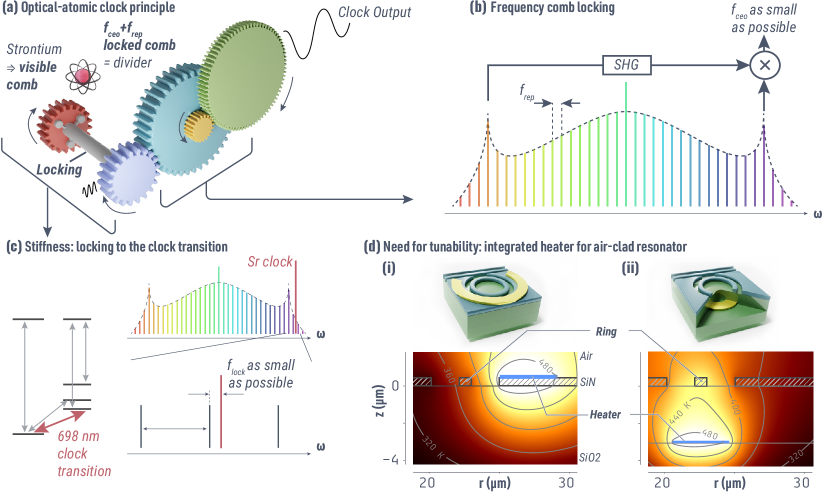
The use of air-clad devices is, however, desirable for dispersion engineering to reach atomic transition frequencies in the short near-infrared and near-visible Moille et al. (2022) and allows for post-fabrication processing to tune the geometrical dispersion if needed Moille et al. (2021a). Direct integration of the heater to the side of the ring results in poor heat build-up at the ring core [Fig. 1(d.i)], caused by the air trenches that act as an insulator but are essential to create the ring during the lithography and etch fabrication steps. The alternative approach we propose in this paper is to bury the integrated heater below the ring resonator [Fig. 1(d,ii)], where a few micrometer gap of silica separates the metal from the optical layer, resulting in no change in the ring losses. Due to the continuous path for heat transfer between the heater and ring layers, the efficiency of such a buried heater is much higher than for the lateral one, confirmed by thermal simulation [Fig. 1(d)]. We demonstrate the fabrication of such unique integrated heaters, which are wire-bonding ready for integration in optical clock systems. In addition, fully embedding the heater in silica and subsequently planarizing the silica layer makes the remainder of the fabrication process compatible with a typical Si photonics process flow Thomson et al. (2016). We experimentally show the high tuning efficiency of the system, where a resonator mode shift of 1.5 THz (equal to 1.5 the resonator free spectral range (FSR)) is achieved without degradation of the resonator quality factor and with limited cross-talk. While tuning of air-clad resonators has numerous potential applications, including in sensing and coupling to quantum emitters, we showcase the utility of these heaters in the context of broadband DKS microcombs. We experimentally demonstrate tunability of the microcomb with an estimated shift of of 15 % of the FSR and an estimated shift of the locked optical clock frequency of close to 2 FSR, while little modification to dispersion – and hence the DW position – occurs.
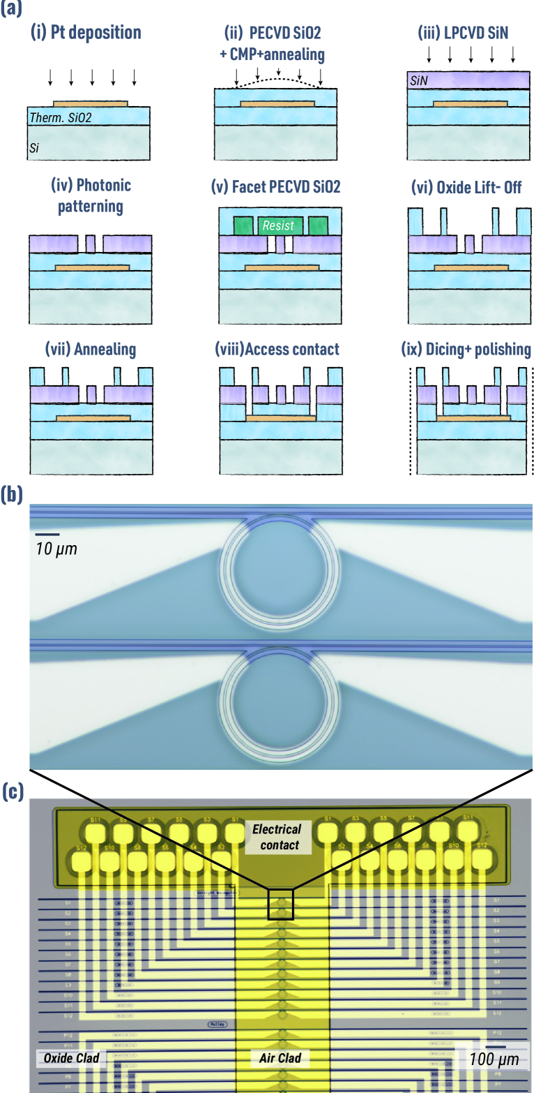
The fabrication of the system [Fig. 2(a)] starts with a standard commercial silicon substrate with a 3 µm thick thermal oxide. We then define the heater pattern using a direct-write lithography maskless aligner (MLA) NIS [Fig. 2(a-i)]. The platinum is then deposited (electorn beam evaporation) and lifted off. Another layer of 2.8 µm of SiO2 is deposited above the heater layer using a 180 °C low temperature High Density Plasma Chemical Vapor Deposition (HDPCVD) process [Fig. 2(a-ii)]. To allow for the best material and the lowest absorption, we proceed to anneal the wafer at 1000 °C for three hours. Thanks to the low diffusivity of metal into silica McBrayer, Swanson, and Sigmon (1986), the buried heater remains geometrically intact and the silica layer exhibits low absoprtion after the annealing. A chemical-mechanical polishing (CMP) step [Fig. 2(a-ii)] is done to create a flat surface before low-pressure chemical vapor deposition (LPCVD) of a 430 nm thick film of silicon nitride Moille et al. (2021b) [Fig. 2(a-iii)]. From this point on, the process is the same as our regular nano-patterning and fabrication of air-clad ring resonators Moille et al. (2021a). The ring resonator patterns are created through electron-beam lithography, with the patterns aligned to the underlying buried heaters using metal alignment marks that are created within the heater layer. The electron-beam resist is used as a mask for a CHF3 reactive ion etch (RIE) of the silicon nitride [Fig. 2(a-iv)]. In order to maintain an air-clad ring resonator for dispersion purposes while allowing for low insertion losses, a lift-off of low temperature HDPCVD SiO2 using nLOF resist is performed [Fig. 2(a-v,vi)]. A last annealing step is performed to anneal the silicon nitride film, which has been shown to reduce absorption in the C-band through reducing N-H bonds Stein, Peercy, and Sokel (1983) [Fig. 2(a-vii)]. Finally, an inductively coupled plasma (ICP) etch through the silicon nitride and the substrate silica, combined with a one minute 6:1 buffer oxide etch dip, reveals the metal layer for electrical contact [Fig. 2(a-viii)]. The chip is then diced and polished for optical testing [Fig. 2(a-ix)].
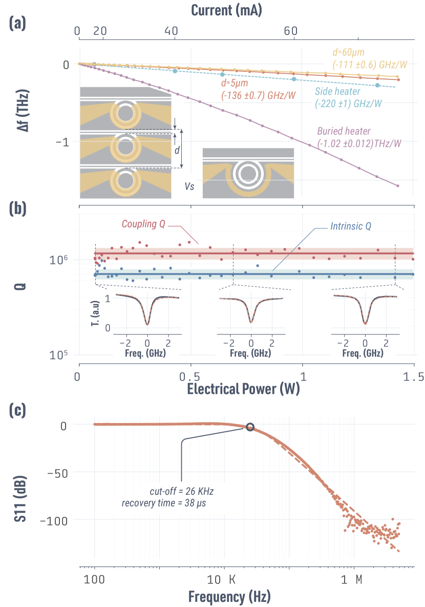
We proceed to characterize the linear performance – spectral tuning, cross talk and speed – of the buried integrated heater. The experimental setup consists of a continuous tunable laser (CTL) around 970 nm probing a single resonant mode of the cavity. The chip is placed on an aluminum sample holder not thermally connected to the optical table (see supplementary material). Heaters are addressed from the electrical pads with DC probes connected to a current source, which can produce output up to 1.5W of electrical power. We measure the electrical resistance of the integrated heater to be , of the same order of magnitude as typical integrated heaters Xue et al. (2016); Joshi et al. (2016). Injecting 1.2 W of electrical power (i.e. a current of 67 mA), we measure a frequency shift of the resonance of more than 1.5 THz, corresponding to an FSR red-shift [Fig. 3(a)]; amongst other things, this guarantees the ability to tune one of the microresonator’s modes onto resonance with any fixed pump laser wavelength. From simulations (see supplementary materials) this frequency shift is consistent with an increase in temperature at the ring above 900 K. We note that this frequency shift is quite large compared to state-of-the art integrated heaters in the silicon nitride nonlinear photonics platform that can be obtained through foundry fabrication Rao et al. (2021) where a shift of only of an FSR was achieved for the same electrical power. The efficiency of the buried heater is THz/W, an improvement by a factor 5 compared to the lateral heater efficiency of GHz/W. The uncertainty estimation arises from the standard deviation in the confidence interval for the linear fit of the frequency shift with electrical power. In addition, the cross talk of the integrated heater is limited. The next ring resonator, with its closest point from the neighboring active heater of about 5 µm – a relatively tight separation considering the waveguide access needed to optically address the resonator – only show a thermal shift of GHz/W. Therefore, the cross-talk of our system can simply be defined by %. Interestingly, the cross talk is not highly dependent with the distance from the heater. Indeed, the second neighbor from the active heater shows a spectral shift of GHz/W, showing that a significant portion of the chip is heating. Therefore, cross-talk could be further improved through an appropriate thermal shunt through the backside of the chip.
We proceed to consider the impact of the buried heater on the optical quality factor of the ring resonator [Fig. 3(b)]. We found that the intrinsic quality factor, in addition to being similar to that of our regular fabrication without the metal layer of Moille et al. (2021a), remains unchanged for any temperature and electrical power applied to the system. Moreover, we measure that the coupling quality factor stays fixed at any temperature, highlighting the little thermal expansion of the system, resulting in a fixed geometry with temperature. Our coupling is based on a straight waveguide, but in the future, using pulley-like coupling, which is more sensitive to geometrical variations Moille et al. (2019a), would give a better estimate to what extent the thermal expansion is truly negligible. We also performed dynamical measurements, in the small signal regime using a vector network analyzer, to measure the recovery time of the buried heater and the frequency up to which the system can function [Fig. 3(c)]. It exhibits a 3 dB cut-off at about 26 kHz, which corresponds to a recovery time of the system of 38 µs. It is worth noting that this value is similar to that of integrated heaters on top of silica-clad rings Xue et al. (2016), and is essentially limited by the thermal lifetimes of silicon nitride and silica Li et al. (2017).
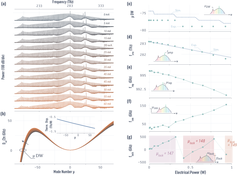
The integrated buried heater presented here shows a high efficiency with a large thermo-refractive mediated spectral shift of the resonant mode. It remains to characterize how the thermal tuning of a ring resonator impact the metric associated with the optical atomic clock frequency comb , namely , and . In previous work, it has been demonstrated that thermal tuning of the ring resonator allows for small tuning of the the microcomb repetition rate Xue et al. (2016). Here, we also proceed to characterize others metrics, to assess the impact of the thermal tuning on the cavity dispersion, the carrier envelop offset and the locking frequency, which represent three other important quantities for efficient microcomb application in optical atomic clocks. To do so, we create dissipative Kerr soliton microcombs at different electric powers [Fig. 4(a)]. Interestingly, the overall shape of the frequency comb remains mostly the same, with only a slight shift of the DW position, despite the introduction of another dispersion contribution. Indeed, the variation of the effective refractive index with temperature is wavelength-dependent given the discrepancy in the thermo-refractive coefficient between Si3N4 ( K-1) Elshaari et al. (2016); Moille et al. (2019b), SiO2 ( K-1) Elshaari et al. (2016) and air ( K-1) and the variation of the effective mode area, which decreases with higher frequency (or mode number) [Fig. 4(b)]. The integrated dispersion, as obtained from finite element method simulations taking into account Joule heating, temperature distribution, and the thermo-refractive coefficient (see supplementary materials), shows only a slight modification across the thermal tuning range. Therefore, the dispersive waves – essential for achieving octave spans and self-referencing of a microcomb – would remain mostly unchanged despite variation of the above parameters. As reported in Fig. 4(c), the experimental DW shift is only 2 modes, from to , and shows a slight discrepancy from finite element method simulations ( to ). Although the overall shape of the DKS microcomb remains unchanged, its fundamental characteristics of relevance for clock applications – repetition rate and carrier-envelope offset frequency – are tuned with the electrical power injected. As seen previously, the resonances are red-shifted with the electrical power, ergo the pump frequency is also red-shifted [Fig. 4(d)]. As the refractive index of the material increases with the temperature, the group index should also increase, resulting in a lower repetition rate of the DKS circulating in the resonator, as measured experimentally [Fig. 4(e)]. Given the repetition rate shift and the shift of the pump resonance, it is expected that will also vary. We extract it from the measurements of and as , where is the integer that brings within the range [-,+], and find that tuning of more than 100 GHz (i.e about 10% of ) is achievable [Fig. 4(f)]. This tuning can be crucial to allow for to be shifted into a detection bandwidth of a photodetector. Finally, we demonstrate the possibility of tuning to a stabilized optical reference [Fig. 4(g)]. Here, we have assumed a comb tooth is present near the 85Sr transition at 698 nm. In practice, our demonstrated combs in this work do not extend to this wavelength due to poor comb extraction resulting from the straight waveguide coupling scheme employed Moille et al. (2019a); however, we have demonstrated similar combs (without heaters) extending to 698 nm using optimized pulley couplers Moille et al. (2022). Finally, we note that because the comb tooth mode order is large, it provides a large multiplicative factor on the temperature-induced shift in . Thus, with only 1 W of electrical power, shifts across 3 different comb teeth, constituting a span .
We have demonstrated a new technique to integrate efficient micro-heaters on chip, with an air-cladding resonator, by burying the heater below the optical device layer. Once the buried heater is patterned, encased in SiO2, and planarized, the subsequent process flow is the same as for standard Si3N4 photonic devices. We show that such buried heater is 5 more efficient than lateral heaters and exhibits low cross-talk which could be even further improved by proper thermal shunt of the chip. We then demonstrate use of the heaters with broadband microcombs, and measure/extract tuning of critical comb parameters for use in optical atomic clocks. While the microcomb measurements are indicative of the use of the buried heater technology for nonlinear integrated photonics applications, we envision many other uses in scenarios for which air cladding are required. This in particular would include microresonator-based sensors Yu et al. (2021) and cavity QED experiments with gas-phase atoms O’Brien, Furusawa, and Vučković (2009); Chang et al. (2020), where both the wide tuning range and negligible impact on resonator quality factor are important factors.
Data availability
The data that supports the plots within this paper and other findings of this study are available from the corresponding authors upon reasonable request.
Acknowledgements
The author thanks Nikolai Klimov and Feng Zhou for valuable inputs. The authors acknowledge partial funding support from the DARPA APHI, DARPA SAVaNT, and NIST-on-a-chip programs.
References
- Dutt et al. (2018) A. Dutt, C. Joshi, X. Ji, J. Cardenas, Y. Okawachi, K. Luke, A. L. Gaeta, and M. Lipson, Science Advances 4, e1701858 (2018).
- Newman et al. (2019) Z. L. Newman, V. Maurice, T. Drake, J. R. Stone, T. C. Briles, D. T. Spencer, C. Fredrick, Q. Li, D. Westly, B. R. Ilic, B. Shen, M.-G. Suh, K. Y. Yang, C. Johnson, D. M. S. Johnson, L. Hollberg, K. J. Vahala, K. Srinivasan, S. A. Diddams, J. Kitching, S. B. Papp, and M. T. Hummon, Optica 6, 680 (2019).
- Spencer et al. (2018) D. T. Spencer, T. Drake, T. C. Briles, J. Stone, L. C. Sinclair, C. Fredrick, Q. Li, D. Westly, B. R. Ilic, A. Bluestone, N. Volet, T. Komljenovic, L. Chang, S. H. Lee, D. Y. Oh, M.-G. Suh, K. Y. Yang, M. H. P. Pfeiffer, T. J. Kippenberg, E. Norberg, L. Theogarajan, K. Vahala, N. R. Newbury, K. Srinivasan, J. E. Bowers, S. A. Diddams, and S. B. Papp, Nature 557, 81 (2018).
- Suh and Vahala (2018) M.-G. Suh and K. J. Vahala, Science (New York, N.Y.) 359, 884 (2018).
- Leo et al. (2010) F. Leo, S. Coen, P. Kockaert, S.-P. Gorza, P. Emplit, and M. Haelterman, Nature Photonics 4, 471 (2010).
- Herr et al. (2014) T. Herr, V. Brasch, J. D. Jost, C. Y. Wang, N. M. Kondratiev, M. L. Gorodetsky, and T. J. Kippenberg, Nature Photonics 8, 145 (2014).
- Xue et al. (2015) X. Xue, Y. Xuan, Y. Liu, P.-H. Wang, S. Chen, J. Wang, D. E. Leaird, M. Qi, and A. M. Weiner, Nature Photonics 9, 594 (2015).
- Li et al. (2017) Q. Li, T. C. Briles, D. A. Westly, T. E. Drake, J. R. Stone, B. R. Ilic, S. A. Diddams, S. B. Papp, and K. Srinivasan, Optica 4, 193 (2017).
- Guo et al. (2017) H. Guo, M. Karpov, E. Lucas, A. Kordts, M. H. P. Pfeiffer, V. Brasch, G. Lihachev, V. E. Lobanov, M. L. Gorodetsky, and T. J. Kippenberg, Nature Physics 13, 94 (2017).
- Moille et al. (2020) G. Moille, L. Chang, W. Xie, A. Rao, X. Lu, M. Davanco, J. E. Bowers, and K. Srinivasan, Lasers & Photonics Reviews 14, 2000022 (2020).
- Stern et al. (2018) B. Stern, X. Ji, Y. Okawachi, A. L. Gaeta, and M. Lipson, Nature 562, 401 (2018).
- Ye et al. (2022) Z. Ye, F. Lei, K. Twayana, M. Girardi, P. A. Andrekson, and V. Torres-Company, Laser & Photonics Reviews 16, 2100147 (2022).
- Diddams, Vahala, and Udem (2020) S. A. Diddams, K. Vahala, and T. Udem, Science (New York, N.Y.) 369, eaay3676 (2020).
- Yu et al. (2019) S.-P. Yu, T. C. Briles, G. T. Moille, X. Lu, S. A. Diddams, K. Srinivasan, and S. B. Papp, Physical Review Applied 11, 044017 (2019).
- Drake et al. (2019) T. E. Drake, T. C. Briles, J. R. Stone, D. T. Spencer, D. R. Carlson, D. D. Hickstein, Q. Li, D. Westly, K. Srinivasan, S. A. Diddams, and S. B. Papp, Physical Review X 9, 031023 (2019).
- Bosman and Havinga (1963) A. J. Bosman and E. E. Havinga, Physical Review 129, 1593 (1963).
- Xue et al. (2016) X. Xue, Y. Xuan, C. Wang, P.-H. Wang, Y. Liu, B. Niu, D. E. Leaird, M. Qi, and A. M. Weiner, Optics Express 24, 687 (2016).
- Joshi et al. (2016) C. Joshi, J. K. Jang, K. Luke, X. Ji, S. A. Miller, A. Klenner, Y. Okawachi, M. Lipson, and A. L. Gaeta, Optics Letters 41, 2565 (2016).
- Helgason et al. (2021) Ó. B. Helgason, F. R. Arteaga-Sierra, Z. Ye, K. Twayana, P. A. Andrekson, M. Karlsson, J. Schröder, and Victor Torres-Company, Nature Photonics 15, 305 (2021).
- Tikan et al. (2021) A. Tikan, J. Riemensberger, K. Komagata, S. Hönl, M. Churaev, C. Skehan, H. Guo, R. N. Wang, J. Liu, P. Seidler, and T. J. Kippenberg, Nature Physics 17, 604 (2021).
- Moille et al. (2022) G. Moille, D. Westly, G. Simlegor, and K. Srinivasan, in CLEO: Science and Innovations (Optica Publishing Group, 2022) pp. SW4H–6.
- Moille et al. (2021a) G. Moille, D. Westly, N. G. Orji, and K. Srinivasan, Applied Physics Letters 119, 121103 (2021a).
- Thomson et al. (2016) D. Thomson, A. Zilkie, J. E. Bowers, T. Komljenovic, G. T. Reed, L. Vivien, D. Marris-Morini, E. Cassan, L. Virot, J.-M. Fédéli, J.-M. Hartmann, J. H. Schmid, D.-X. Xu, F. Boeuf, P. O’Brien, G. Z. Mashanovich, and M. Nedeljkovic, Journal of Optics 18, 073003 (2016).
- (24) Certain commercial products or names are identified to foster understanding. Such identification does not constitute recommendation or endorsement by the National Institute of Standards and Technology, nor is it intended to imply that the products or names identified are necessarily the best available for the purpose.
- McBrayer, Swanson, and Sigmon (1986) J. D. McBrayer, R. M. Swanson, and T. W. Sigmon, Journal of The Electrochemical Society 133, 1242 (1986).
- Moille et al. (2021b) G. Moille, G. Moille, D. Westly, G. Simelgor, K. Srinivasan, and K. Srinivasan, Optics Letters 46, 5970 (2021b).
- Stein, Peercy, and Sokel (1983) H. J. Stein, P. S. Peercy, and R. J. Sokel, Thin Solid Films 101, 291 (1983).
- Rao et al. (2021) A. Rao, G. Moille, X. Lu, D. A. Westly, D. Sacchetto, M. Geiselmann, M. Zervas, S. B. Papp, J. Bowers, and K. Srinivasan, Light: Science & Applications 10, 109 (2021).
- Moille et al. (2019a) G. Moille, Q. Li, T. C. Briles, S.-P. Yu, T. Drake, X. Lu, A. Rao, D. Westly, S. B. Papp, and K. Srinivasan, Optics Letters 44, 4737 (2019a).
- Elshaari et al. (2016) A. W. Elshaari, I. E. Zadeh, K. D. Jons, and V. Zwiller, IEEE Photonics Journal 8, 1 (2016).
- Moille et al. (2019b) G. Moille, X. Lu, A. Rao, Q. Li, D. A. Westly, L. Ranzani, S. B. Papp, M. Soltani, and K. Srinivasan, Physical Review Applied 12, 034057 (2019b).
- Yu et al. (2021) D. Yu, M. Humar, K. Meserve, R. C. Bailey, S. N. Chormaic, and F. Vollmer, Nature Reviews Methods Primers 1, 83 (2021).
- O’Brien, Furusawa, and Vučković (2009) J. L. O’Brien, A. Furusawa, and J. Vučković, Nature Photonics 3, 687 (2009).
- Chang et al. (2020) T.-H. Chang, X. Zhou, M. Zhu, B. M. Fields, and C.-L. Hung, Applied Physics Letters 117, 174001 (2020).
Experimental Setup
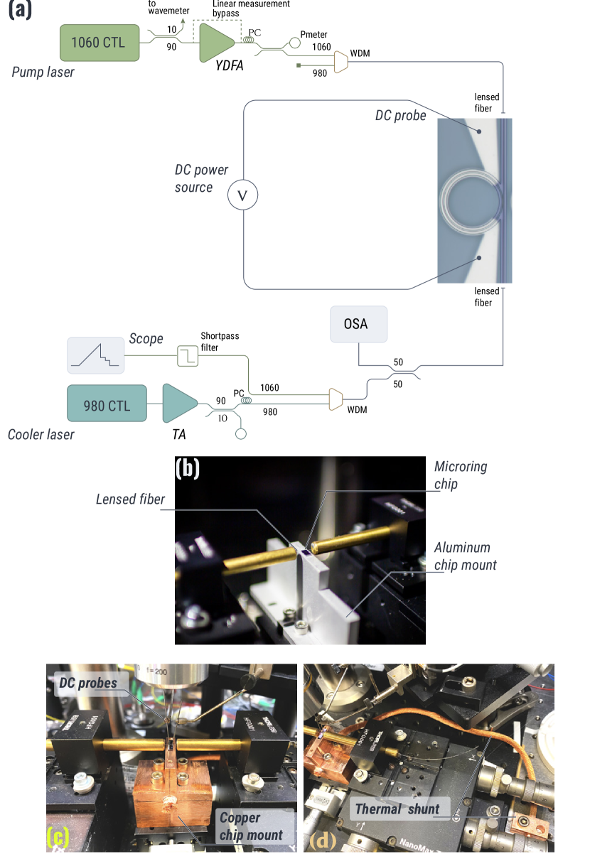
The setup used in this work is presented schematically in Fig. S1(a). The continuously tunable laser (CTL) provides tuning of the wavelength from 1010 nm to 1070 nm to perform spectroscopy, and we adjust the input light polarization such that we excite the the fundamental transverse electric (TE) modes (i.e., TE0) of the resonator, by measuring the transmission as a function of wavelength. In this linear case, the sample mount is made of aluminum (Fig. S1(b)), through which we noticed experimentally a limited heat diffusion and an overal increase of the chip temperature, resulting in coupling instability for creation of DKS. In contrast, we use a copper sample mount linked to the optical table(Fig. S1(c)-(d)) to perform nonlinear measurements, where an ytterbium-doped fiber amplifier (YDFA) is used to produce adequate optical power around 1060 nm, while a (counterpropagating and orthogonally polarized) 980 nm laser is used to actively cool the resonator to reach states adiabatically. With its improved thermal conductivity and heat sinking to the optical table so that the impact of the buried heaters is more local and the overall chip temperature is not increased as much as in the case of the Al sample mount. Importantly, the overall frequency tuning range achieved by the buried heater is nearly the same regardless of the mount (i.e., comparing Fig. 3(a) and Fig. 4(d)). Interestingly, we believe that use of the copper mount also helps mitigate convective air flows, making the setup much more stable. This has allowed us to measure the DKS states at different electrical powers in Fig. 4 without the need to adjust the fiber position for optical coupling.
Thermal Simulations
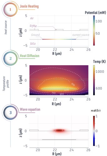
In order to accurately account for the integrated buried heater impact on the optical mode of the ring resonator, we performed so called fully-coupled simulations, where the Joule heating, heat diffusion and wave equations are solved as a coupled equations system [Fig. S2]. First, we leverage the symmetry of the system, where in a cylindrical coordinate system , periodic boundary conditions are assumed in , simplifying the system to an effective two-dimensional one along . The optical field is given as , with the azimuthal mode number of the ring resonance. Although the implemented heater design breaks this symmetry because it was not fully wrapped around the ring to avoid heating of the resonator-waveguide coupling region, we will assume the heat diffusion is strong enough to allow for uniform temperature in . Here, we describe the essential steps taken by the solver, although these equations are effectively solved simultaneously. We start by simulating Joule heating, where a current density is injected in the heater assuming the measured resistance of 260 [Fig. S2(a)], which we use as a heat power source for the heat diffusion equation [Fig. S2(b)], allowing us to retrieve the temperature profile along . The boundary conditions are crucial for accurate simulation, and following the improvement of the setup described in the previous section, we assume the bottom of the substrate to be at room temperature and the others as open boundaries. Simulations where the substrate thickness has been increased did not significantly change the simulations results. Although the bottom of the substrate may present a higher temperature than the one assumed here, our assumption of room temperature best reproduces the experimental data presented in Fig. 4. Finally, using a Seillmeier model to determine the refractive index of the silicon nitride and silicon dioxide layers according to ellipsometry measurements previously performed Moille et al. (2021b), and accounting for the thermo-refractive index coefficient of each material, we use the simulated profile to determine the refractive index shift due to the heating. This allows to model the frequency shift of a given resonator mode along with complete dispersion of the resonator modes with electrical power.