Mapping quantum Hall edge states in graphene by scanning tunneling microscopy
Abstract
Quantum Hall edge states are the paradigmatic example of the bulk-boundary correspondence. They are prone to intricate reconstructions calling for their detailed investigation at high spatial resolution. Here, we map quantum Hall edge states of monolayer graphene at a magnetic field of 7 T with scanning tunneling microscopy. Our graphene sample features a gate-tunable lateral interface between areas of different filling factor. We compare the results with detailed tight-binding calculations quantitatively accounting for the perturbation by the tip induced quantum dot. We find that an adequate choice of gate voltage allows for mapping the edge state pattern with little perturbation. We observe extended compressible regions, the antinodal structure of edge states and their meandering along the lateral interface.
I Introduction
The quantum Hall (QH) effect v. Klitzing et al. (1980) initiated the topological description of electron systems in solids Thouless et al. (1982); Kohmoto (1985); Niu et al. (1985). The principle of bulk-boundary correspondence attributes the bulk related Chern number to edge states carrying the dissipationless Hall current.Halperin (1982); Hatsugai (1993); Graf and Porta (2013) This revolutionary insight triggered more detailed investigations of the spatial structure of the edge states in the presence of Coulomb interactions, starting with calculations of the widths of compressible and incompressible stripes.Chklovskii et al. (1992); Lier and Gerhardts (1994) Later, complex reconstructions including charged and neutral upstream modes have been predicted at filling factor Khanna et al. (2021); Venkatachalam et al. (2012); Bhattacharyya et al. (2019) and in the fractional QH regime.MacDonald (1990); Kane et al. (1994); Wan et al. (2003); Wang et al. (2013) The neutral upstream modes have partially been evidenced indirectly via their shot noise properties.Bid et al. (2010); Sabo et al. (2017) For graphene, upstream modes can also appear due to the bare gate electrostatics at the rim of the graphene flake.Marguerite et al. (2019); Moreau et al. (2021) Moreover, a fragmentation of integer QH edge states by exchange interactions has been predicted.Oswald (2021); Oswald and Römer (2017a, b) These intriguing predictions and indirect experimental results call for a more detailed spatial investigation of QH edge states in real space.
Initial studies used a scanning single electron transistor Yacoby et al. (1999) as well as electrostatic force microscopy McCormick et al. (1999); Weitz et al. (2000); Weis and von Klitzing (2011) to evidence the presence of edge states. Later, scanning gate microscopy,Aoki et al. (2005); Paradiso et al. (2012); Pascher et al. (2014) scanning capacitance microscopy,Suddards et al. (2012), microwave impedance microscopy,Lai et al. (2011) and scanning SQUID microscopy Uri et al. (2019) have been employed. However, all of these methods provide a spatial resolution well above the magnetic length, such that the internal structure of the edge states remained elusive. Indirectly, macroscopic tunneling experiments probed the internal structure via the in-plane field dependence, but only for rather steep potential profiles without signatures of reconstruction and, naturally, without any information on the edge state pattern along the edge.Patlatiuk et al. (2020) Hence, higher resolution scanning probes are mandatory for this purpose. They can be favorably applied to graphene with its exposed surface.Andrei et al. (2012); Morgenstern (2011) Indeed, imaging of quantum Hall edge states by scanning tunneling microscopy (STM) has been attempted at a graphene boundary, but on a strongly screening graphite substrate that naturally suppresses any edge state evolution.Li et al. (2013) More recently, a gated lateral interface of graphene on h-BN has been employed to realize more soft confinement,Kim et al. (2021) enabling the visualization of symmetry broken edge states by Kelvin probe force microscopy. Nevertheless, the internal internal edge state structure has remained elusive.
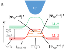
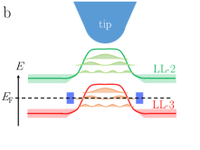
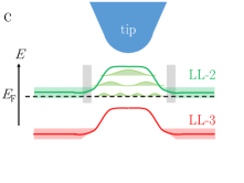
Here, we apply scanning tunneling microscopy (STM) in a perpendicular magnetic field T Mashoff et al. (2009) probing an interface between different filling factors. The well-known Landau level (LL) pinning at the Fermi level as function of gate voltage Jung et al. (2011); J. Chae, S. Jung, A. F. Young, C. R. Dean, L. Wang, Y. Gao, K. Watanabe, T. Taniguchi, J. Hone, K. L. Shepard, P. Kim, N. B. Zhitenev, and J. A. Stroscio (2012); Walkup et al. (2020) causes LL plateaus across the interface indicating the appearance of compressible stripes.Chklovskii et al. (1992); Lier and Gerhardts (1994) As a major challenge, the electrostatic potential of the tip itself induces a quantum dot immediately below the tip.Dombrowski et al. (1999); Freitag et al. (2016) This tip-induced quantum dot (TIQD) can significantly affect the measurement, locally disturbing the edge-state structure one hopes to measure. Here, we use experimentally observed charging lines to deduce the parameters determining width and depth of the TIQD in detail.Freitag et al. (2016, 2018) We thereby set up a tight-binding (TB) model that quantitatively accounts for the local electrostatics around the tip, and hence include effects of the TIQD. Comparing the measured signal as function of , sample voltage and position to our simulations allows us to identify parameter regimes where the perturbation due to the TIQD is minimal, enabling the spatial mapping of the edge states with unprecedented resolution.
In detail, we calculate the local density of states (LDOS) below the tip center as we virtually move the TIQD across the interface at T. Our model reproduces all features found in the experiment and, hence, enables a direct comparison with the spatial LDOS distribution for each tip position . We find that the dominant lines of are caused by states of the TIQD. However, weaker branching-type features at the interface represent the barely perturbed edge states with inner anti-nodal structure.Ando (1984); Joynt and Prange (1984); Bindel et al. (2017) Using this novel insight, we measure the spatial distribution of the edge states for various LLs. They show the antinodal structure of LL wave functions that is slightly modified by the potential gradient at the interface and likely also by the electron-electron repulsion. Moreover, the first hole-type LL edge state is mapped along the interface revealing the expected meandering and a spatial variation of its internal structure.
II Experimental Setup
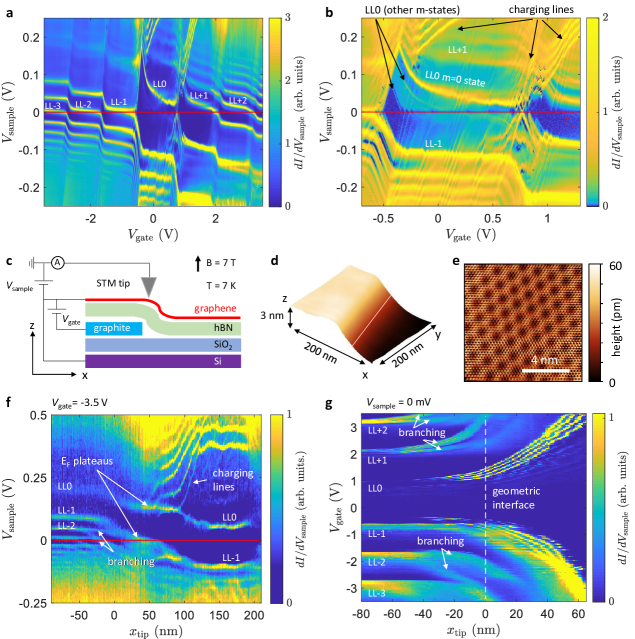
We prepare the graphene sample by the dry stacking method depositing a sequence of 3 nm thick graphite, 23 nm thick hBN and a monolayer graphene exfoliated from graphite on top of Si/SiO2 (Fig. 1c). The graphene is placed partially above the graphite flake to create a tunable potential step (Fig. 1c). Graphite and graphene are contacted by Au electrodes via shadow mask evaporation (Appendix Section VI.1). An STM operating at 7 K in ultrahigh vacuum up to T probes the LDOS at varying applied to the graphite, i.e. potential drop across the interface.Mashoff et al. (2009) An additional voltage is applied to the graphene with respect to the grounded tip that records the tunneling current (Fig. 1c). The recorded by lock-in technique is (to first order) proportional to the LDOS at energy .Morgenstern et al. (2000a) An additional numerical derivative improves the visibility of the charging lines.
III Computational Details
For the TB calculations, we use a nearest-neighbour hopping model Schattauer et al. (2020) for a rectangular single layer graphene flake (220 nm400 nm) reading
| (1) |
where is the on-site energy at site , are hopping parameters between site and site , ( ) are creation (annihilation) operators at site , and the field is included via a Peierls phase
| (2) |
with the magnetic flux , positions , of sites , , and the vector potential in Landau gauge . To simulate the large dimensions of the experimental flake, we employ a rescaled graphene Hamiltonian.Liu et al. (2015) It increases the interatomic distances by a factor of ten and accordingly reduces the dimension of the Hamiltonian without qualitatively altering the energy spectra. This approximation holds since we do not expect the lattice scale of graphene to be relevant at the large scale of the TIQD ( nm) and the magnetic length ( nm).Liu et al. (2015)
IV Results
IV.1 Spectroscopy at a Single Location
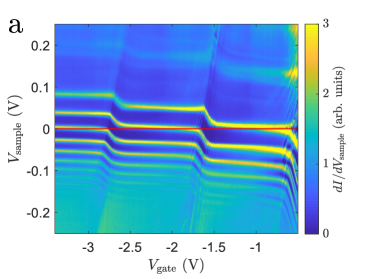
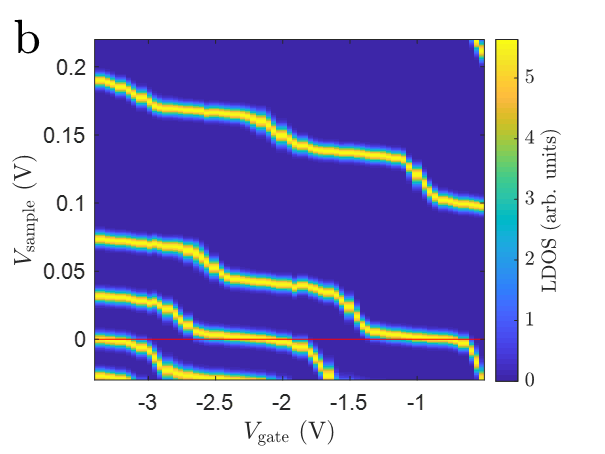
Figure 1a–b shows recorded at a tip location above the graphite gate far away from the interface ( T). States belonging to the Landau levels LL () are visible as bright LDOS lines that feature steps in the plane caused by the pinning of LLs to .Jung et al. (2011); Luican et al. (2011); J. Chae, S. Jung, A. F. Young, C. R. Dean, L. Wang, Y. Gao, K. Watanabe, T. Taniguchi, J. Hone, K. L. Shepard, P. Kim, N. B. Zhitenev, and J. A. Stroscio (2012) The LL indices are identified by the mutual energy distance of the lines and are accordingly marked. Plateaus appear close to at hole doping ( V), but show up at an energy distinct from at electron doping and for LL0.Jung et al. (2011) This implies that the measured LDOS lines are not caused by the intrinsic LLs of the unperturbed graphene bulk, but rather by states of the TIQD.Dombrowski et al. (1999) The confined states of a quantum dot in field are roughly classified for each LL by their different azimuthal quantum numbers (Appendix Section VI.5).Schnez et al. (2008); Freitag et al. (2016) The most prominent LDOS line belongs to the ()-state Morgenstern et al. (2000b); Freitag et al. (2016) as the only one with an antinode in the TIQD center,Schnez et al. (2008) where the tip is probing (Appendix Section VI.5). Additional weaker lines in run in parallel to the ()-state of LL0 at lower (Fig. 1b, zoom-in at larger contrast in Fig. 20). They correspond to ()-states with higher confinement energy.Schnez et al. (2008) The fact that the ()-states are below the ()-state classifies the TIQD as hole-type (Appendix Sections VI.3-VI.5). The apparent plateaus of the -states are eventually caused by the pinning of the bulk LLs of graphene at . The pinning prohibits a strong change of the TIQD depth by . Hence, the plateaus at for V imply that the ()-state of the TIQD is barely displaced energetically from the corresponding bulk LL, i.e. the depth of the TIQD is shallow.
Besides the LDOS lines belonging to -states of different LL, the measured curves (Fig. 1a–b) feature additional lines that are tilted oppositely to the LDOS lines (lines marked ”charging lines” in Fig. 1b) . They are charging lines Jung et al. (2011); Freitag et al. (2016); J. Chae, S. Jung, A. F. Young, C. R. Dean, L. Wang, Y. Gao, K. Watanabe, T. Taniguchi, J. Hone, K. L. Shepard, P. Kim, N. B. Zhitenev, and J. A. Stroscio (2012); Walkup et al. (2020) with a slope caused by the positive gate voltage compensating a negative tip voltage (hence a positive ) to keep the charge in the TIQD constant. Such charging lines are known to be caused by the Coulomb staircase effect,Freitag et al. (2016, 2018) i.e., each additional electron added to the TIQD changes the LDOS and thus the measured current abruptly by Coulomb repulsion. The jumps in the LDOS associated with these charging events thus appear prominently in scanning tunneling spectroscopy (Fig. 1b), e.g., the ()-states of LL0 and LL-1 exhibit kinks wherever a charging line crosses (see also Fig. 20, appendix). Some charging lines exhibit quadruplets with regular distances as expected from the fourfold degeneracy of graphene (Appendix Section VI.9).Freitag et al. (2016)
The most prominent charging lines cross the LDOS features marked LL at the right end of their plateaus at (Fig. 1a, b, Fig. 21, appendix). Weaker charging lines follow towards the left (i.e., for smaller . This again classifies the TIQD as hole-type,Jung et al. (2011) since the ()-state is charged firstly with highest impact on the probed LDOS due to its antinode directly below the tip (Appendix Section VI.3). A more negative removes further electrons, i.e. charges holes into higher -states of the TIQD, that feature a larger average lateral distance to the tip center and, hence, induce less changes of the LDOS below the tip. We use the charging lines to determine energetic depth and lateral width of the TIQD below.
IV.2 Spectroscopy across the Interface
The sample geometry (Fig. 1c) enables a lateral interface of different filling factors via a partial graphite gate that changes the carrier density in the graphene area on the left. The position of the interface is determined by STM as a visible step of the graphite height within the graphene layer (Fig. 1d). The graphene is strongly rotated () with respect to the underlying hBN (Fig. 1e) minimizing the influence of the moiré structure on the TIQD states.Freitag et al. (2016, 2018)
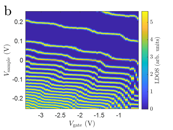
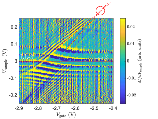
Moving the STM tip across the interface while varying or reveals the evolution of the Landau level energies across the interface (Fig. 1f and g) . On the left (right) in Fig. 1f, is between LL-4 and LL-3 (LL-1 and LL0). Hence, filling factors are different as intended. The LL-1 state exhibits a plateau at close to the interface ( nm). This demonstrates a lateral pinning of the bulk LL-1 to typically dubbed a compressible stripe Chklovskii et al. (1992) and a rather shallow TIQD. For the unoccupied LL0 state, we observe a similar plateau, but slightly shifted to the right (arrows labeled ” plateaus” in Fig. 1f). This confirms the flat potential area caused by the compressible stripe and demonstrates a change of the compressible stripe position by the TIQD, respectively. Almost horizontal charging lines appear in the upper right of Fig. 1f highlighting the charging of LL-1 states that are pulled across by positive .Hashimoto et al. (2008) The evolution of these charging lines along directly probes the potential Hashimoto et al. (2008) and hence again confirms the rather flat potential areas in the interface region ( nm) as expected for compressible stripes as well as surrounding steeper potentials featuring the separating incompressible stripes.Chklovskii et al. (1992); Lier and Gerhardts (1994) The three charging lines that subsequently propagate along the LDOS plateau of LL0 (label ”charging lines” in Fig. 1f) showcase, moreover, the charge carrier density gradient at constant potential as expected for compressible stripes.Chklovskii et al. (1992) Finally, we find an unexpected branching of the LL-2 and LL-1 line around nm that we analyze in detail below. Notice that a branching of LLs has also been observed for topological insulator states within a remote Coulomb potential, where could not be applied.Fu et al. (2014) It has been attributed to a similar origin as in our analysis, i.e. to the antinodal structure of the LL wave functions.Fu et al. (2014)
We next consider the evolution of at (V) across the interface for varying height of the potential step by tuning (Fig. 1g). The strongest influence is observed on the left side () as expected, where many LL cross . However, the gate continues to influence LL features, at least, up to nm, to the right of the graphite gate, albeit to a weaker extent. Quadruplets of lines are partially observed, e.g. in the upper right, implying a strong influence of the charging of the TIQD at the corresponding voltages. More interestingly, a pronounced branching of the LL states across the interface appears again for LL+2, LL+1, and LL-2 (labels ”branching” in Fig. 1g). The branching is barely visible for LL-1 exhibiting only a shoulder at the left of the main intensity. This is due to the interference of charging lines. But the branching of LL-1 is clearly apparent in two-dimensional maps of this LL at , where a double line is meandering along the interface (Fig. 4c).
IV.3 Tight Binding Simulations Including the Tip Induced Quantum Dot
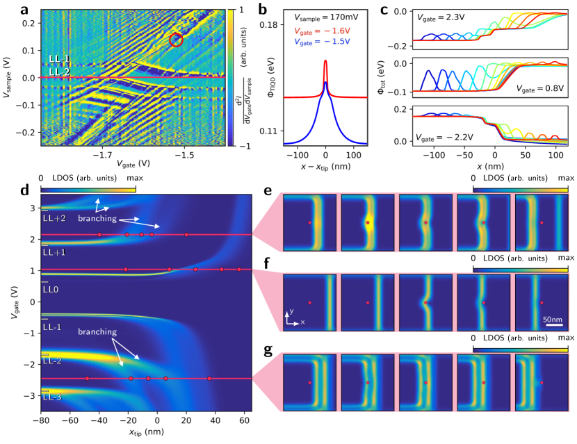
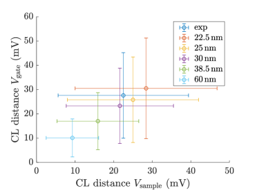
In order to explain the observed branching of various LL at the interface, we perform TB simulations employing a realistic potential. The potential is deduced from Poisson simulations with parameters extracted from the experimental charging lines. We consider the work function mismatch between graphene and the tip as well as between graphene and the graphite gate and (assuming an approximately spherical tip) the radius of the tip apex (Appendix Section VI.2). The work function mismatches are quantified as voltages and required for charge neutrality of the graphene and flat band conditions below the tip, respectively. These parameters can be deduced from the first crossing points of charging lines originating from adjacent LL (Fig. 2a). Such a crossing implies a potential depth of the TIQD identical to the energy difference between the two LL (Fig. 9d, appendix). Using two such crossing points at two pairs of (, ), we straightforwardly determine mV and mV by comparison with Poisson simulations (Appendix Section VI.3). The parameter nm is deduced from the average distance of charging lines again by comparison with the Poisson simulations (Appendix Section VI.3).
Two resulting TIQD potentials (far away from the lateral interface) are shown in Fig. 2b. The complete lateral potential including TIQD and interface potential results from a Poisson simulation using the geometry of Fig. 1c as well as the known , , , , , and (Appendix Section VI.4). The potential features multiple steps across the interface due to alternating compressible and incompressible stripes (Fig. 2c, lower and upper frame).Chklovskii et al. (1992); Lier and Gerhardts (1994)
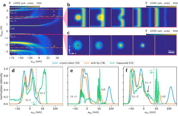
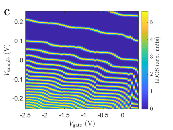
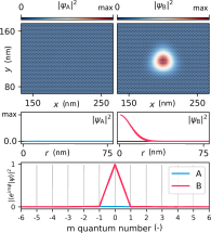
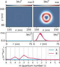
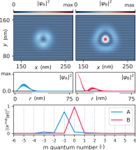
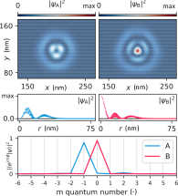
These potentials, adequately transformed into 2D potentials (Appendix Section VI.6), are the input for the TB simulations. We construct the LDOS from the resulting single particle states: we sum all states around the energy selected by in an energy window of meV in order to capture the temperature broadening in the experiment.Morgenstern et al. (2000a) Spatially, we average across a circular region (radius nm) around the 2D tip center position to account for a possible mismatch between the tunneling position and the capacitive center of the tip. Morgenstern et al. (2000b) Figure 2d shows the resulting LDOS for a direct comparison to Fig. 1g. Crucially, the branching features of the various LL states are correctly reproduced, while LL0 does not exhibit any branching. The favorable agreement calls for a detailed study of the complete LDOS map at various as naturally provided by the TB simulations. The calculations reveal that the branching is a consequence of the internal structure of the edge state wave functions at the interface (Fig. 2e–g). For example, the edge state belonging to LL-2 (Fig. 2g) exhibits two antinodes that are probed by the tip as two arms of a branching of the LL-2 state (Fig. 2d). By contrast, the edge state of LL0 with a single antinode (Fig. 2f) does not show branching in the probed LDOS of Fig. 2d. A local displacement of the edge state by the TIQD potential (apparent in Fig. 2e–g) only shifts the lateral position of the edge state center with minor influence on its internal structure (see below).
Figure 3b–c reveals instead that the intense horizontal LDOS lines observed to the far left of the lateral interface (Fig. 3a) are caused by states of the TIQD. These states are shifted in energy across the interface and, hence, can disappear from the probed energy window. Thus, only the weaker LDOS features across the interface contain the desired edge state information.
IV.4 Direct Comparison of Experimental and Simulated Data
To elucidate the remaining influence of the TIQD, we now directly compare the calculated cross-section of the LDOS related to the edge states (blue lines in Fig. 3) to the measured (green lines) and to the simulated including the TIQD (orange lines). Favorably, the twofold antinodal structure of LL-2 (Fig. 3d) and LL+2 (Fig. 3f) appears very similarly in all three curves, i.e. peak distances and relative intensities are alike. This good agreement for LL-2 can be traced back to the fact that the TIQD is absent at the interface region (Fig. 2c, lower frame,nmnm). Analyzing the distance of antinodes in more detail reveals nm in the experiment largely independent of . In the TB calculations with TIQD, we find nm slightly decreasing with increasing . A 1D TB calculation representing the overlapped unperturbed LL wave functions of the two sublattices finds nm (Appendix Section VI.8), i.e. the experimental distance of antinodes is larger by %. Slightly larger distances in the experiment are also observed for LL+1 (Fig. 3e), with values largely independent from in experiment ( nm) and simulations ( nm) (Appendix Section VI.8), and for LL+2 (Fig. 3f). The larger distances in the experiment could be due to the neglected electron-electron repulsion in the TB calculation. In a perturbation theory approach, Coulomb repulsion would mix the states at with higher LLs, compensating the energy cost for partial occupation of higher LLs by the gain in Coulomb energy due to the increased lateral extension of the states at . Finally, we note the slight variation in peak heights of the LL edge states in Fig. 3d-f. For example, the first of the two peaks of the LL-2 feature in Fig. 3d is slightly lower in intensity than the second in both experiment and theory. This variation is caused by, both, the presence of the TIQD (compare relative peak heights of the orange and blue lines), and by the finite slope of the potential at the interface (Appendix Section VI.8).
Discrepancies in relative intensities of antinodal peaks get, however, significant, if charging lines interfere (LL0 in Fig. 3e–f). The peak distances in Fig. 3e still match reasonably between green and orange lines, but not the relative peak intensities. More severely, the distances between the edge state peaks of LL+1 (LL+2) and LL0 (Fig. 3e (f)) are considerably reduced by the presence of the TIQD (blue vs. orange lines). This relates to a shift of the most right incompressible stripe towards the left by the superposed TIQD potential (Fig. 2c, upper frame). Nevertheless, the simulated shift of LL0 by the TIQD (orange) is in quantitative agreement with the experiment (green). The fact that the LL-1 feature in Fig. 3d strongly deviates from the simulated peak in terms of position and intensity is likely related to the interfering charging lines (Fig. 1g) of a relatively shallow TIQD (Fig. 2c, lower frame, nm). In such a shallow TIQD, individual charging events can strongly change the TIQD potential, an effect not captured by the simulations. Thus, imaging of the edge states works best if no charging lines are observed in the corresponding parameter regime and the TIQD is absent in the region of the lateral interface.
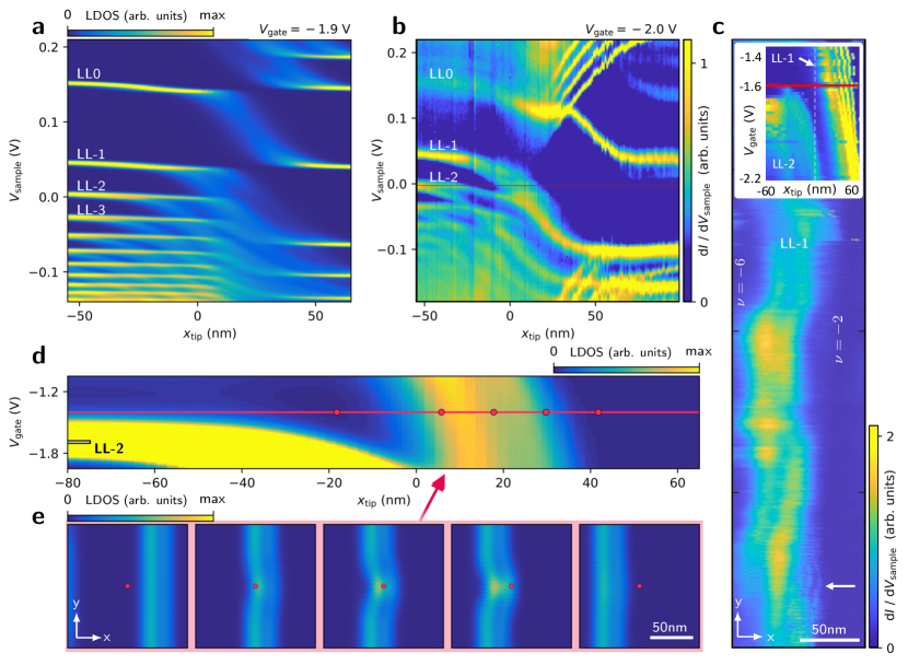
IV.5 Mapping the Edge State
To corroborate the generally good agreement between measured and simulated LDOS, we compare their dependence on and in Fig. 4a–b (see also Fig. 19). Again, one observes semi-quantitative agreement including the branching features of LL-1 to LL-3. At a slightly smaller , only LL-1 crosses at the interface (red line in inset of Fig. 4c). At this , we map two-dimensionally at (Fig. 4c). A bright line about 40 nm in width with some internal structure meanders along the lateral interface. Mostly, the bright line is a double line structure as expected for LL-1 (compare TB simulation of Fig. 3e showing LL+1) Width and internal structure of this stripe are rather similar to the simulated LDOS() of the LL-1 edge state (Fig. 4d, along red line). An analysis of the correspondingly mapped LDOS (Fig. 4e) reveals that the observed double line is due to the intrinsic double line of the LL-1 edge state, itself caused by the antinodal structure of the LL-1 wave function that is barely perturbed by the shallow TIQD. In some areas, as marked by the white arrow in Fig. 3c, we observe additional charging lines (see also inset) due to the local potential that changes the occupation of the TIQD, but these areas are small at the chosen .
Hence, an imaging of an edge state with resolution well below the magnetic length nm and only minor perturbations by the TIQD is achieved for the first time.
V Conclusions
We conclude that quantum Hall edge states can be mapped without significant perturbations if one selects favorable parameter regimes. One attractive option to identify such regions is a direct comparison of across a gated lateral interface with TB simulations accounting for the TIQD. Crucially, reliable parameters for simulating the TIQD can be straightforwardly deduced from the measured charging lines in . Current limitations of the method include neglecting confinement effects on the shape of the TIQD, which would require more time-consuming Poisson-Schrödinger simulations and, probably more severe, the assumption of a circularly symmetric TIQD. Trial and error-type control on the TIQD shape, however, can generally be achieved by mapping the capacitive charging of a point defect.Morgenstern et al. (2000b); Teichmann et al. (2008) Even with these limitations, the antinodal structure of the edge states could be mapped in a largely quantitative fashion, even revealing the influence of the potential gradient at the interface on the relative peak heights. An additional gate that can also tune the filling factor on the other side of the interface might eventually give access to multiple nearly unperturbed edge states including some that separate symmetry broken Wang et al. (2022) or fractional QH phases.
During the final preparation of this manuscript, we became aware of measurements attempting to probe quantum Hall edge states at the physical edge of graphene on hBN/SiO2/Si. They did not find signatures of edge states, again likely due to a too strong edge potential.Coissard et al. (2022)
Author Contributions
T.J. provided the idea of the experiment and performed the experimental measurements as well as the Poisson simulations, supervised by M.M. and S.S.. A.W. and M.H prepared the sample supervised by R.G.. C.S. provided the tight-binding simulations supervised by F.L.. M.M. conceived and supervised the project. All authors discussed the results and co-wrote the manuscript.
Competing Interests
The authors declare no competing interests.
Acknowledgements
We gratefully acknowledge helpful discussions with T. Fabian, V. Falko and M. Goerbig. This project has received funding from the European Union’s Horizon 2020 research and innovation programme under grant agreement number 881603 (Graphene Flagship, Core 3) and by the German Science foundation via Mo 858/16-1 as well as Mo 858/15-1. We further acknowledge support from the FWF DACH project I3827-N36 and COST action CA18234. Christoph Schattauer acknowledges support as a recipient of a DOC fellowship of the Austrian Academy of Sciences. Numerical calculations were in part performed on the Vienna Scientific Cluster VSC4. Roman Gorbachev acknowledges support from Royal Society, ERC Consolidator grant QTWIST (101001515) and EPSRC grant number EP/V007033/1.
VI Appendix
VI.1 Sample Preparation, Locating the Lateral Interface by STM and Measuring the STS Signal
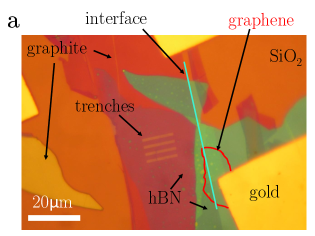
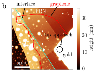
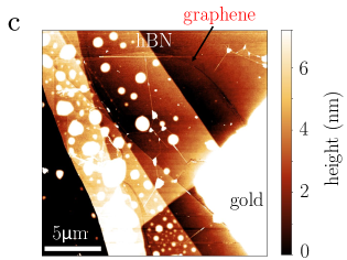
The sample is prepared by firstly exfoliating a graphite flake onto a Si/SiO2 chip. Afterwards, two hBN flakes and a graphene flake are transferred onto the graphite by dry stacking such that the graphene only partially covers the graphite.Kretinin et al. (2014) Finally, the graphene and the graphite are electrically contacted. For this purpose, a shadow mask is fixed on the chip through which 60 nm high gold contacts are evaporated by a thermal gold evaporator. An optical image of the sample is shown in Fig. 5a and atomic force microscopy (AFM) images are provided in Fig. 5b–c. The chip with the sample is then glued onto a STM sample holder. The graphene flake and the Si back gate are connected to the sample holder with silver paint. One additional contact connects the graphite flake independently via a gold wire. After loading the sample into the STM of the ultrahigh vacuum chamber, the tip is positioned onto the corner of the gold contact next to the graphene flake (Fig. 5b) using an optical long-distance microscope for monitoring. Then, the tip is approached until tunneling current is achieved. The tip is afterwards moved laterally towards the graphene flake while continuously recording the topography. It is easy to recognize the graphene, since the gold is significantly more rough. With the tip on the graphene, the lateral interface is eventually identified by a 3 nm high step resulting from the underlying graphite (Fig. 1d, main text).
For STM and scanning tunneling spectroscopy (STS), we used an etched W wire that is prepared on W(110) by voltage pulses until a reliable curve and stable were obtained. After maneuvering the tip to the graphene, additional mild voltage pulses are applied on the Au contact pads next to the graphene to get rid of possible dirt that is picked up during the path towards the graphene. We did not use other tip materials to tune the tip work function, since variations of the work function for the same material due to different facets at the tip apex can amount to up to 250 meV already.Dombrowski et al. (1999) For STS, the voltage is applied to the graphene and the tunneling current is recorded at the tip. Lock-in technique probes after opening the feedback loop at voltage and current . The modulation frequency is Hz for all images except Figs. 1f, 4b, main text, and Figs. 19b, 22, where we used Hz. The modulation amplitude is mV except for Figs. 1f, 4b, main text, and Figs. 19b, 22, where it is mV.
VI.2 Poisson Simulation
To perform tight binding (TB) calculations for comparison with STS, we need the 2D potential profile on the graphene around the interface. It consists of the potential step induced by the graphite gate and the tip induced quantum dot (TIQD) caused by the potential difference between tip and sample. The potentials are due to the applied voltages between graphite gate and graphene as well as between the tip and graphene (Fig. 1c, main text) and the corresponding work function mismatches. Moreover, the geometry of these two metallic electrodes and the density of states (DOS) of the graphene are relevant.
For estimating the resulting potential, we employ numerical Poisson calculations. The home-made Poisson solver uses either 2D Cartesian coordinates or coordinates for a 3D cylindrical symmetry. The calculations disregard confinement effects, i.e. we do not use a Poisson-Schrödinger solver. Instead, we treat the DOS as a property that is rigidly shifted by the local potential. The Landau level structure of the DOS as well as the temperature via the Fermi-Dirac distribution are taken into account.Freitag et al. (2016)
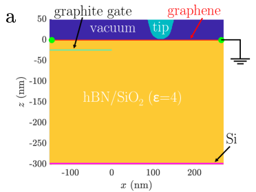
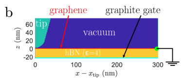
Fig. 6 shows the chosen geometries for the Poisson simulations. They are largely identical to Fig. 1c, main text, except that the graphite is two-dimensional without extension in -direction. The thickness of the hBN nm is deduced from atomic force microscopy (AFM) images. Both, hBN and SiO2 are described by their dielectric bulk constant . We choose a reasonable value nm for the distance between graphene and the tip apex since it barely influences the results.Freitag et al. (2016, 2018); Morgenstern et al. (2000a) The tip is assumed to be metallic with a shape consisting of a half sphere with radius located at the lower end of a cone with opening angle .
The graphite is set to a potential , where C. is the applied gate voltage and is the required gate voltage to achieve charge neutrality in the graphene. In the Poisson simulations, the sample is grounded and the tip is set to a variable potential . This is different from the experiment, where the tip is grounded. The reason is that the sample grounding at the graphene edge enables a more straightforward implementation of the Poisson solver.Freitag et al. (2016) The tip potential, hence, reads ) with applied graphene voltage and being the voltage required to achieve flat band conditions below the tip for eV.
The used Landau level (LL) DOS employs a Fermi velocity m/s leading to LL energies:Neto et al. (2009)
| (3) |
with the magnetic field perpendicular to the graphene and the Landau level index. A Gaussian broadening of the Landau levels with FWHM of meV is additionally applied.

We eventually plot a simulated LDOS(, ) derived from the LDOS of graphene directly below the tip center at the energy with respect to the Fermi level of the sample that matches (Fig. 7b, c). This enables a comparison with the measured (, ) (Fig. 7a) and, hence, an optimization of parameters (see below).
The agreement between Fig. 7a and c is reasonable, i.e the same LLs are crossing in the experimental range at similar . However, details are different, e.g. the lengths of the plateaus are shorter in the simulation. This can be improved by adapting as an additional fit parameter (Fig. 8) taking into account that the dipolar screening of hBN and SiO2 is modified at its surfaces. We omit such additional fit parameter in the following to keep the number of fit parameters low and, thus, the reasoning more transparent.
VI.3 Determining the Parameters for the Poisson Simulation
As decisive parameters for the Poisson simulations, we need to determine , and . For this purpose, we use the observed charging lines in at nm, i.e far away from the lateral interface (Fig. 1a-b, main text). The charging lines are directly related to the TIQD potential. The tip radius correlates with the lateral size of the TIQD, i.e. with the distance of charging lines, whereas and affect the potential depth of the TIQD, i.e. the onset of charging lines for each LL.
These crucial parameters are determined as follows. The sign of is given by the experimentally observed ()-states of LL0 that appear at lower energy than the ()-state, itself identified as the line with strongest intensity (Fig. 1b, main text). This is only possible, if the ()-state is confined in a QD potential maximum implying a hole-type QD (Fig. 9a). Additionally, the observation that the strongest lines of the -states are pinned above , for LL0, LL+1 and LL+2, is consistent with a hole-type TIQD where the ()-states are separated upwards in energy from the bulk LL pinned at (Fig. 9c).
A more detailed consideration of the negative area of Fig. 1a, main text, reveals crossings of charging lines originating from different LL (Fig. 2a, main text, and Fig. 10). The attribution of a charging line to LL uses its intersection with a LL LDOS feature at ( V). Hence, the charging lines on the left in Fig. 10 originate from LL-3. They represent the first few holes of LL-3 that are added to the TIQD. The very first LL-3 hole is marked by a dashed line. Close to the crossing of this charging line with , LL-3 of the surrounding graphene must be completely occupied with electrons (Fig. 9b), since the filling factor of the surrounding graphene must always be larger than the filling factor of a hole-type TIQD. Either, of the surrounding graphene is in the gap between LL-3 and LL-2 (Fig. 9b) or it is at states of the rim of LL-3 that are known to be localized.Joynt and Prange (1984); Ando (1984) Both situations provide an insulating barrier for the confined charge carriers in the TIQD, such that screening of the added charge is strongly suppressed. Consequently, a strong change of the DOS by charging the TIQD results in a bright charging line.
The charging lines appearing on the right of Fig. 10 belong to the last holes from LL-2 that are charged into the TIQD. They exhibit a steeper slope since these states are, on average, located further away from the capacitive center of the tip (Fig. 9). In the surrounding bulk, must be located within LL-2, again since the filling factor of the bulk must be larger than the local filling factor of a hole-type TIQD (Fig. 9c).
The crossing point of two charging lines from LL-3 and LL-2 implies that QD states from both LLs are at simultaneously. This is naturally realized by a ring like charge distribution with occupied hole states including the first state from LL-3 in a central disk and occupied hole states only from LL-2 in an annulus around the disk (Fig. 9d). Such configuration is quite usual for QDs in field and sometimes called a wedding cake.Gutiérrez et al. (2018) The wedding cake scenario is also found in our Poisson simulations (not shown).
The situation of Fig. 9d can be used to estimate the TIQD depth. Since LL-2 is at in the surrounding bulk, the QD depth approximately equals the known energy gap between LL-2 and LL-3 of 30.5 meV (eq. 3). Here, we ignore the finite energetic width of the bulk Landau levels since not being a dominant error. For the transition from LL-1 to LL-2, a crossing of charging lines is also observed (Fig. 2a, main text) implying a TIQD depth at this point of 38.9 meV. From these two crossing points at two distinct pairs of and , we eventually determine and .
Practically, we firstly measure the experimental voltage differences between the two crossing points, V in direction and V in direction. Then, we determine the depth of the TIQD potential from the Poisson simulations at varying and (Fig. 11a) using circular symmetric coordinates (Fig. 6a). Afterwards, we select all (, ) that exhibit the potential depths as present during the crossing points in the experiment (color code in Fig. 11b). Subsequently, we find pairs of (, ) that feature the two TIQD depths at the two crossing points (38.9 meV, 30.5 meV) and, at the same time, the energetic distances in and that are identical to the voltage distances between the two crossing points ( V, V). The found pairs are marked as symbols of the same color in Fig. 11.
This still leaves us with two possibilities. To select the correct one, we compare the two pairs of two () with the respective two (, ) of the two crossing points to determine their offsets, and . Then, we compare the resulting calculated LDOS(, ) for both cases with the measured (Fig. 7). This leads to a straightforward selection of the the red pair within Fig. 11 corresponding to mV and mV. The relatively large error of these values results from the selected step size of 100 meV in and within the Poisson simulations.
The remaining fit parameter is deduced from the distance of the charging lines in the experiment by comparison with the Poisson simulations. In the Poisson simulations, we determine the additional charge within the TIQD, , that is caused by a potential change in direction or in direction. Note that is directly the capacitance of the TIQD with respect to the gate as often used for analyzing quantum dots in transport experiments.Thomas Ihn (2010) The total charge within the TIQD is calculated by spatially integrating the confined charge carrier density up to the edge of the TIQD. The edge separates the TIQD from the surrounding bulk with constant filling factor and, hence, can include an outer insulating (incompressible) ring of the TIQD where the potential is still changing (blue areas in Fig. 9b). Eventually, we compare and for various with the experimental number of charging lines per voltage (Fig. 12). For this purpose, we select groups of charging lines with regular voltage distances implying only minor contributions from orbital energy, i.e., from the confinement energy neglected in the Poisson simulations. We determine their average distance and use the average of all such groups for V and V. This voltage area is selected since the simulated LDOS data at V matches the experiment favorably (Fig. 7) and since each charging line should only contribute once. The preselection of groups of regular charging lines also deals with the fact that some of the charging lines might not be visible due to imperfect confinement at or strong screening from the surrounding graphene.
Practically, we firstly estimate by adapting the ratio of to the corresponding ratio of the experiment (slope of the charging lines) and latter refine via the agreement of absolute values of and with the experimental ones. The parameter is varied until the absolute values fit favorably resulting in nm (Fig. 12). We finally check for consistency by repeating the determination of and with the found (Fig. 11). However, we find that these two values barely depend on .
In principle, the Poisson simulations also reveal the charge in the TIQD for each . Hence, one could add lines to Fig. 7b–c at integer multiples of in the TIQD in order to also reproduce the charging lines. We crosschecked that this partially matches the experiments, but generally would overemphasize the accuracy of our model.
VI.4 Poisson Simulation Including the Lateral Interface
For determining the full potential profile across the interface in presence of the TIQD, we employ 2D Cartesian coordinates that neglect the direction along the interface (Fig. 6a). We crosschecked that this 2D restriction gives the same result as the 3D calculation of the TIQD using cylindrical symmetry far away from the interface. The potential profile is determined using the geometry as depicted in Fig. 6a and employs the determined , , and . We perform simulations for multiple positions of the tip while varying and (e.g. Fig. 2c, main text).
VI.5 Tight Binding Model of the Tip Induced Quantum Dot
Before discussing the TB simulations of the lateral interface with TIQD, we describe the TB results for the TIQD without interface. Fig. 13a sketches the investigated large graphene flake with chosen zigzag and armchair edges. A center position of the TIQD is marked at in horizontal direction. In vertical direction, the TIQD is always centered in the middle of the flake. Fig. 13b shows the resulting energy spectrum with 2500 states for the graphene rectangle without TIQD at T. The corresponding density of states (DOS) (inset of Fig. 13b) reveals pronounced Landau quantization with peak energies according to eq. (3). We adapted the energy scale to account for the slightly different deduced from the LL energy distance in experiment ( m/s) and resulting from our -nearest-neighbour TB parameters ( m/s).
Next, we add the potential of the TIQD with center at the marked position . We use a fit function found previously Freitag et al. (2018); Schattauer et al. (2020); Schnez et al. (2008) reading
| (4) | |||
| (5) |
with being the 2D position on the flake with respect to . The parameter is taken in Å, while is taken in eV. For demonstration in Fig. 5c, we use a potential depth eV, but later and are fit parameters that are optimized to reproduce the potential profiles from the Poisson simulations.
The resulting energy spectrum of the flake with TIQD consists of eigenstates where the localized quantum dot states are energetically separated from the LL energies (eq. 3). Fig. 14 displays some of these states. They showcase the typical sublattice-dependent structure that appears for graphene LLs at each valley or .Neto et al. (2009) The index describes the conventional LL wave functions and, hence, differs by one between the two sublattice components reading
| (6) |
with being the classical LL wave functions. For , the other component vanishes.
To analyze the calculated confined states within the TIQD, we energetically separate these sublattice structures by numerically breaking valley degeneracy with a potential in sublattice space reading .Freitag et al. (2018, 2016).
For quantum dots with a spherical infinite mass boundary or with zig-zag boundaries of the continuum Dirac-Weyl Hamiltonian, one gets well-defined radial and azimuthal quantum numbers and , respectively, that are related to the LL index via Schnez et al. (2008)
| (7) |
for infinte mass boundary conditions or via
| (8) |
for zig-zag boundary conditions with Heavyside function . Note that each state that belongs to a particular LL is uniquely defined by the index .
Albeit this model is not entirely applicable to our boundary conditions, we analyze the TIQD states accordingly (Fig. 14). The number of radial nodes is easily determined by inspecting the radial density distribution (middle row of Fig. 14a–d). The angular quantum number is more tricky. We first have to account for the Bloch phase depending on the valley index (, ). Since our confinement potential is smooth, valley is still a good quantum number as verified by inspecting the localization of Husimi distributions in reciprocal space (not shown). After removing the Bloch phase, we select a slim annular region around the global, radial maximum of each state. After renormalizing within this area, we calculate the overlap integrals with test functions of the form , , where is the azimuthal angle calculated with respect to the TIQD center. A large overlap as in Figs. 14a, c, d, bottom rows, indicates a well-defined quantum number of the corresponding TIQD states. This is, however, not always the case as, e.g., in Fig. 14b, bottom row, exhibiting two relevant overlaps. The discrepancy is likely due to effects of trigonal warping that are additionally enhanced by the applied artificial enlargement of the unit cell. Moreover, we find that the conditions of eqs. 7 and 8 do partially not hold. Nevertheless, for the sake of simplicity, we dub the states found in the experimental data as states of a particular LL in order to stress the central antinode of the state that is most strongly visible in the STM data and is also found consistently for different LL in the TB simulations (e.g. Figs. 14a, c, d, right column, top and bottom row).
VI.6 Transferring the 1D Poisson Simulation to the 2D Potential of the Tight Binding Model
Next we use the results from the 1D Poisson simulations to obtain a 2D potential as base for the TB model. For ease of implementation, we use analytic fit functions.
We parameterize the total potential as
| (9) |
The argument of the quench function is a superposition of the TIQD potential and the lateral interface potential. The TIQD potential reads (eq. 4)
| (10) | |||
| (11) |
with Fermi function . The tip position is given in units of Å and the resulting in units of eV.
The one-dimensional potential across the lateral interface is modelled by
also with energies in eV and position parameters in Å.
To incorporate the flattened regions of the interface potential (compressible stripes) resulting from the Poisson solver (Fig. 15a), we adapt a quench function within eq. (9) that locally modifies the potential values by subtracting Gaussians from the unperturbed weight factor of one,
| (13) |
with Gaussians along the direction. The Gaussians are centered at , with a standard deviation and a height . Here, represents the unquenched potential. The , , with [LL, …, LL+4 ] are fit parameters describing the flat potential areas (compressible regions) for each LL. To compare with the experimental data, we account for and by adequate energy shifts.
The resulting potential reproduces all of the relevant features generated by the Poisson solution (Figs. 15a,b). This includes the variations of depth and lateral size of the TIQD across the lateral interface as well as the flat potential regions appearing when LL energies cross . Even complex features such as a pronounced shift of the interface potential step by the TIQD are rather well reproduced (brackets in Fig. 15, left row). A quantitative comparison is shown for three examples in Fig. 16 revealing deviations in the few meV regime that we regard as irrelevant considering the uncertainties of the Poisson simulations (section VI.2–VI.4) such as the neglected confinement energies within the TIQD and the assumption of a circular symmetric tip.
Since is two-dimensional by construction, the 2D shape of the TIQD is apparent while traversing the lateral interface (not shown). It develops from a circular symmetric TIQD on the left of the interface with shape depending on via an elongated, somewhat skewed TIQD at the interface into an again circular TIQD to the right of the interface, here with depth and shape largely independent of , but depending on .
The simulated LDOS() without TIQD (blue lines in Fig. 3d–f, main text) results from a single TB simulation of LDOS(, ) with (eq. 9) and setting .
VI.7 Interpolations within the Tight Binding Simulations
Poisson simulations are performed for a grid of 22 different and 14 different . In the TB simulations we obtain densely sampled plots of the LDOS(, ) by employing an interpolation scheme shifting the calculated LDOS below the tip rigidly via a local potential shift. While we use a linear interpolation for each (eq. 9) between adjacent , we employ a capacitively motivated interpolation along relying on with describing the inverted capacitance between tip and TIQD. It is used as a fit parameter accounting for the slightly different between experiment and TB model.
For calculations of LDOS(, ) (Fig. 4a, main text, Fig. 19a), we employ a rigid energy shift of the LDOS in the center of the TIQD after calculating it for V by . The lever arm is estimated from the Poisson simulations.
The linear shift is justified by the relatively shallow TIQD with meV. This shallow potential does not enable screening effects originating from different bulk Landau levels at .
VI.8 Additional Comparison between Measured and Simulated Data
Figure 17 shows evaluated lateral distances between the two peaks in the branching features as observed in of Fig. 1g, main text, and LDOS of Fig. 2d, main text. The insets show the relevant areas of the images from the main text. We evaluate the two maxima of and LDOS at various and determine their mutual distances. We concentrate on the edge state features that are not (LL-2) or only weakly (LL+1) perturbed by charging lines in the experiment. Obviously, the experimental distances barely change with as expected for an edge state that originates from the Landau level wave functions within the Landau gauge.Joynt and Prange (1984) The distance is larger for LL-2 as for LL+1 as also expected from the antinodal structure of the corresponding wave functions (Fig. 18a–b). However, the distances found within the tight binding model are smaller by up to 30 % and exhibit a weak trend with . The latter indicates that Landau level wave functions are mixed by the (variation in) slope of the potential as the dot moves across the lateral interface. The origin of the former is unclear, but might be related to electron-electron repulsion that aims to separate electron density maxima and is not included in the tight binding model.
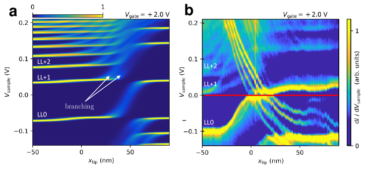
Figure 18a–b shows simplified Landau level wave functions of graphene within a linear potential as calculated by a one-dimensional tight binding model. The slope of the potential ( meV/nm) is chosen in between the slopes observed on the plateaus at the interface within the Poisson simulations ( meV/nm) and the average slope found across the lateral interface ( meV/nm) (Fig. 2c, main text). The additionally displayed two sublattice contributions reveal the well-known one- and two-fold antinodal structure for LL+1 as well as the two- and three-fold antinodal structure for LL-2, representing the chiral symmetry of graphene in analogy to the quantum dot solutions of eqs. (6). However, remarkably, the resulting peaks are different in height showing that the wave functions are not pure Landau gauge solutions, but the solutions are mixed LL wave functions due to the influence of the potential slope. The simplified model nicely reproduces peak distances and relative peak heights of the more complex tight binding simulations that include the detailed potential of the Poisson solver (blue lines in Fig. 18c–d) as well as the ones that additionally consider the TIQD (orange lines in Fig. 18c–d). They also reproduce the trend of different peak heights as found in the experiment, but underestimate the experimental peak distances.
We conclude that the observed edge states are largely given by the Landau gauge wave functions of the two sublattices. However, the interface potential gradient leads to a small LL wave function mixing, that implies a slightly larger (smaller) wave function peak located at the more attractive (repulsive) potential side of the interface. Moreover, it is likely that electron-electron repulsion increases the inter-peak distance again via Landau level mixing. We checked with the 1D tight binding model that potential slopes up to meV/nm do not change the inter-peak distance by more than 1.5 nm and, thus, cannot explain the observed larger distances in the experiment.
Finally, we provide additional data corroborating the good, semi-quantitative agreement between our experiment and the TB simulations including the TIQD. Besides the comparison between experimental data and TB simulations in the main text (Fig. 1g, 2d, 4a–d), a comparison of measured and calculated LDOS(, ) at positive is shown in Fig. 19. As always, the parameters determined in section S2–S3 are used as base providing the potentials for the TB simulations. The positive results in a p-n interface with on the left and on the right of the interface. Again, the general agreement between experimental data and simulations is very good with the exception of the additional charging lines in the experimental data. Most importantly, the branching of LL features is again observed in the experiment and in the simulation, here very pronounced for the LLs.
VI.9 Analysis of (, ) at a Fixed Lateral Position
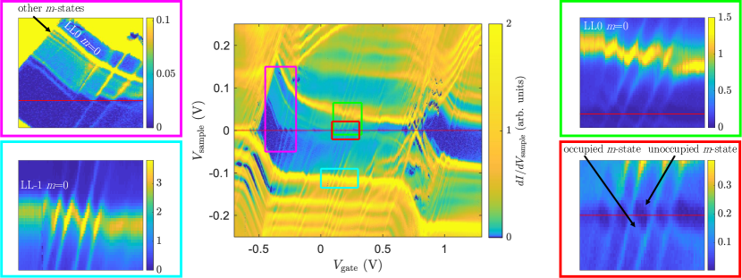
Figure 20 shows several zooms into the map of (, ) as displayed in Fig. 1b, main text, that is recorded at a position far away from the lateral interface. In the upper left corner, the zoom showcases the appearance of several states of LL0 that are confined at different energies within the TIQD. Obviously, these lines largely run in parallel along stressing a similar energy change by the back gate voltage for all of these TIQD states. As discussed in the main text, the brightest line belongs to . It is found at largest rendering the TIQD hole-type. i. e. higher states are at lower energy. Coulomb diamonds appear when the different states cross (red line). The zooms in the lower left and the upper right of Fig. 20 feature the kinks in the LDOS lines of states away from ( V) that appear whenever a charging line is crossing. As described in the main text, this showcases the Coulomb staircase effect, i.e. the LDOS is shifted by the Coulomb repulsion of the additional charge within the TIQD.Freitag et al. (2016) The upper right zoom, moreover, features a quadruplet of rather equidistant charging lines. The four rightmost ones have a similar mutual distance, while the fifth one exhibits a larger distance to the fourth one. This fourfold bunching is caused by the fourfold spin and valley degeneracy of each state in graphene. By following the charging lines down to (red line) and comparison with the central image, it is also apparent that these charging lines mark the charging of a higher state of LL0.
A zoom into the crossing area of these charging lines with (lower right zoom) reveals the so-called Coulomb diamonds rather clearly. They result from the simultaneous crossing of the LDOS features of the -states and the charging lines across . Naturally, the subsequent charging of a single -state must imply the simultaneous presence of unoccupied and occupied versions of the -state, except after filling of the fourth degeneracy level. This is nicely visible as LDOS lines propagating in parallel above and below (arrows). The pair of LDOS lines is separated by the charging voltage that must be provided by the tip to place one more electron into the TIQD. The two state energies increase in parallel for more negative and jump back down if an additional hole is charged into the TIQD, i.e., if a charging line crosses. After four such jumps, the -state is completely empty and the next -state moves towards for charging. Hence, again the four visible Coulomb diamonds in the lower right zoom of Fig. 20 indicate the fourfold degeneracy of the corresponding state in graphene.
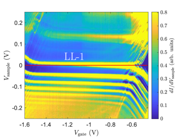
Figure 21 features the plateau at of the LDOS line belonging to LL-1. The most bright charging lines appear on the right end of the plateau followed by weaker charging lines towards the left. As explained in the main text, this supports our classification of the TIQD as a hole-type dot. The ()-state is the one with the highest probability density in the center of the quantum dot and, hence, leads to the strongest charging line by its strongest Coulomb repulsion acting on the states that are probed by the tip. The fact that this ()-state is charged at the largest further corroborates the assignment of the TIQD to a hole-type band bending.
Notice that additional bright charging lines appear in the upper left corner of Fig. 21. They are likely caused by the charging of the ()-state of LL-2.
VI.10 Branching of Landau Levels at Different
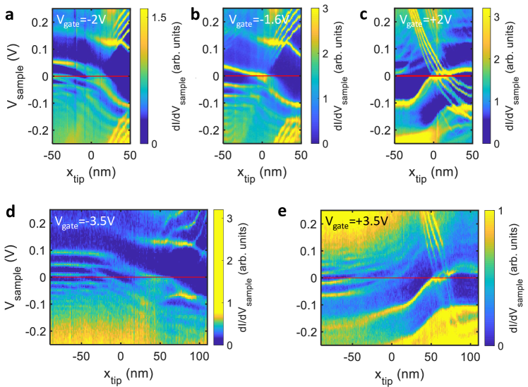
Figure 22 shows the maps across the lateral interface for various applied to the left side of the map areas. The changing filling factor on the left is visible by the number of Landau levels below (red line). The filling factor on the very left changes from at V, i.e. the LL-3 is not occupied with electrons, but LL-4 is occupied, to at V, i.e. LL2 is occupied, but LL3 is not. Moreover, the branching of the LL features appears at all . At negative , the branching looks very similar for different except that the lateral onset of branching is shifted. In contrast, at V, the branching appears to be stronger leading to intersections of different branching lines as in the TB calculations (Fig. 19). In that case, charging lines directly cross the branching areas indicating a strong influence of the TIQD. In turn, in case of weak interference from the TIQD, the branching is rather stable supporting the interpretation that it is caused by the antinodal structure of the edge states at the interface. A more detailed investigation of the strengths of the various branching strengths of occupied and unoccupied LLs as a function of is beyond the scope of this study.
VI.11 Influence of Strain on Branching
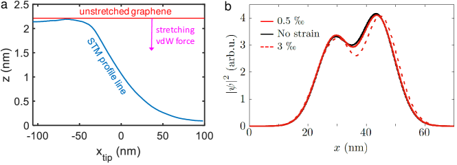
One might wonder, if the presence of the step edge visible in Fig. 1d leads to strain that eventually causes the branching of the LL features in . To exclude such a scenario, we estimate the strain in the following. The step edge visible in Fig. 1d has a height of 2.1 nm and a width of nm according to its line profile (Fig. 23a). The line profile exhibits a continuous curvature with nearly Gaussian shape across the edge. The smooth shape suggests a direct contact of the graphene to the underlying hBN. The graphene is deposited in a separate step after the hBN, such that the hBN already covers the graphite edge prior to graphene transfer. Hence, there is no obvious reason that the graphene should be particularly stretched at the step edge. During transfer, the graphene just sees a minimally bended hBN below. But even if one assumes that the graphene profile develops from a relaxed, initially flat graphene exactly parallel to the SiO2 substrate (red line in Fig. 23a), the resulting strain from stretching it to the measured profile line would be below 0.05 % only. This is roughly the same magnitude as the typical strain fluctuations for graphene samples on flat hBN that exhibit a rms value of 0.05 % as well.Couto et al. (2014); Neumann et al. (2015) Hence, if strain of this small magnitude would cause a peak splitting, such a splitting would appear everywhere, not only at the step edge, in clear contrast to the experiment.
To quantitatively assess the influence of strain on the LL wave functions we consider a strain of 0.05 % as a maximum of a Gaussian profile with full width at half maximum (FWHM) of 60 nm. We modify the hopping parameters accordingly in the TB simulation. We find only minimal changes in the two component Landau level wave function (see Fig. 23b, black vs. red line). The double peak structure barely changes due to this strain. To asses the effect of even larger strain, we increased the strain in the calculation by a factor of six and still found only minor qualitative changes (dashed line, Fig. 23b). For the 1D step edge, we only expect a strain gradient perpendicular to the edge, and thus no pseudomagnetic field that requires a two-dimensional strain distribution.Guinea et al. (2009) However, even if one assumes a circular symmetric Gaussian bump of the same profile as the step, the pseudomagnetic field would be 200 mT only,Guinea et al. (2009); Georgi et al. (2017) much smaller than the externally applied magnetic field (7 T). The difference in Landau quantization due to such a small pseudomagnetic field would result in an energy splitting between the two Dirac cones of meV.Guinea et al. (2009) This unrealistic strain scenario, thus, would still be significantly too small to explain the observed splittings during branching of about 25 meV.
Consequently, we can safely exclude that strain is a major factor for the observed branching of LDOS features at the lateral interface.
References
- v. Klitzing et al. (1980) K. v. Klitzing, G. Dorda, and M. Pepper, “New method for high-accuracy determination of the fine-structure constant based on quantized hall resistance,” Phys. Rev. Lett. 45, 494–497 (1980).
- Thouless et al. (1982) D. J. Thouless, M. Kohmoto, M. P. Nightingale, and M. den Nijs, “Quantized hall conductance in a two-dimensional periodic potential,” Phys. Rev. Lett. 49, 405–408 (1982).
- Kohmoto (1985) Mahito Kohmoto, “Topological invariant and the quantization of the hall conductance,” Ann. Phys. 160, 343–354 (1985).
- Niu et al. (1985) Qian Niu, D. J. Thouless, and Yong-Shi Wu, “Quantized hall conductance as a topological invariant,” Phys. Rev. B 31, 3372–3377 (1985).
- Halperin (1982) B. I. Halperin, “Quantized hall conductance, current-carrying edge states, and the existence of extended states in a two-dimensional disordered potential,” Phy. Rev. B 25, 2185–2190 (1982).
- Hatsugai (1993) Yasuhiro Hatsugai, “Chern number and edge states in the integer quantum hall effect,” Phys. Rev. Lett. 71, 3697–3700 (1993).
- Graf and Porta (2013) Gian Michele Graf and Marcello Porta, “Bulk-edge correspondence for two-dimensional topological insulators,” Comm. Math. Phys. 324, 851–895 (2013).
- Chklovskii et al. (1992) D. B. Chklovskii, B. I. Shklovskii, and L. I. Glazman, “Electrostatics of edge channels,” Phys. Rev. B 46, 4026–4034 (1992).
- Lier and Gerhardts (1994) Karlheinz Lier and Rolf R. Gerhardts, “Self-consistent calculations of edge channels in laterally confined two-dimensional electron systems,” Phys. Rev. B 50, 7757–7767 (1994).
- Khanna et al. (2021) Udit Khanna, Moshe Goldstein, and Yuval Gefen, “Fractional edge reconstruction in integer quantum hall phases,” Phys. Rev. B 103, L121302 (2021).
- Venkatachalam et al. (2012) Vivek Venkatachalam, Sean Hart, Loren Pfeiffer, Ken West, and Amir Yacoby, “Local thermometry of neutral modes on the quantum hall edge,” Nat. Phys. 8, 676–681 (2012).
- Bhattacharyya et al. (2019) Rajarshi Bhattacharyya, Mitali Banerjee, Moty Heiblum, Diana Mahalu, and Vladimir Umansky, “Melting of interference in the fractional quantum hall effect: Appearance of neutral modes,” Phys. Rev. Lett. 122, 246801 (2019).
- MacDonald (1990) A. H. MacDonald, “Edge states in the fractional-quantum-hall-effect regime,” Phys. Rev. Lett. 64, 220–223 (1990).
- Kane et al. (1994) C. L. Kane, Matthew P. A. Fisher, and J. Polchinski, “Randomness at the edge: Theory of quantum hall transport at filling =2/3,” Phys. Rev. Lett. 72, 4129–4132 (1994).
- Wan et al. (2003) Xin Wan, E. H. Rezayi, and Kun Yang, “Edge reconstruction in the fractional quantum hall regime,” Phys. Rev. B 68, 125307 (2003).
- Wang et al. (2013) Jianhui Wang, Yigal Meir, and Yuval Gefen, “Edge reconstruction in the =2/3 fractional quantum hall state,” Phys. Rev.Lett. 111, 246803 (2013).
- Bid et al. (2010) Aveek Bid, N. Ofek, H. Inoue, M. Heiblum, C. L. Kane, V. Umansky, and D. Mahalu, “Observation of neutral modes in the fractional quantum hall regime,” Nature 466, 585–590 (2010).
- Sabo et al. (2017) Ron Sabo, Itamar Gurman, Amir Rosenblatt, Fabien Lafont, Daniel Banitt, Jinhong Park, Moty Heiblum, Yuval Gefen, Vladimir Umansky, and Diana Mahalu, “Edge reconstruction in fractional quantum hall states,” Nat. Phys. 13, 491–496 (2017).
- Marguerite et al. (2019) A. Marguerite, J. Birkbeck, A. Aharon-Steinberg, D. Halbertal, K. Bagani, I. Marcus, Y. Myasoedov, A. K. Geim, D. J. Perello, and E. Zeldov, “Imaging work and dissipation in the quantum hall state in graphene,” Nature 575, 628–633 (2019).
- Moreau et al. (2021) N. Moreau, B. Brun, S. Somanchi, K. Watanabe, T. Taniguchi, C. Stampfer, and B. Hackens, “Upstream modes and antidots poison graphene quantum hall effect,” Nat. Commun. 12, 4265 (2021).
- Oswald (2021) Josef Oswald, “Hybridization of wide compressible edge stripes and narrow quantum channels driven by many body interactions in the quantum hall effect regime,” Results in Physics47, 106381 (2023).
- Oswald and Römer (2017a) Josef Oswald and Rudolf A. Römer, “Manifestation of many-body interactions in the integer quantum hall effect regime,” Phys. Rev. B 96, 125128 (2017a).
- Oswald and Römer (2017b) Josef Oswald and Rudolf A. Römer, “Exchange-mediated dynamic screening in the integer quantum hall effect regime,” Europhys. Lett. 117, 57009 (2017b).
- Yacoby et al. (1999) A Yacoby, H.F Hess, T.A Fulton, L.N Pfeiffer, and K.W West, “Electrical imaging of the quantum hall state,” Sol. St. Comm. 111, 1–13 (1999).
- McCormick et al. (1999) Kent L. McCormick, Michael T. Woodside, Mike Huang, Mingshaw Wu, Paul L. McEuen, Cem Duruoz, and J. S. Harris, “Scanned potential microscopy of edge and bulk currents in the quantum hall regime,” Phys. Rev. B 59, 4654–4657 (1999).
- Weitz et al. (2000) P Weitz, E Ahlswede, J Weis, K.Von Klitzing, and K Eberl, “Hall-potential investigations under quantum hall conditions using scanning force microscopy,” Physica E: Low-dimensional Systems and Nanostructures 6, 247–250 (2000).
- Weis and von Klitzing (2011) J. Weis and K. von Klitzing, “Metrology and microscopic picture of the integer quantum hall effect,” Phil. Trans. Royal Soc. A: Math., Phys. Eng. Sci. 369, 3954–3974 (2011).
- Aoki et al. (2005) N. Aoki, C. R. da Cunha, R. Akis, D. K. Ferry, and Y. Ochiai, “Imaging of integer quantum hall edge state in a quantum point contact via scanning gate microscopy,” Phys. Rev. B 72, 155327 (2005).
- Paradiso et al. (2012) Nicola Paradiso, Stefan Heun, Stefano Roddaro, Lucia Sorba, Fabio Beltram, Giorgio Biasiol, L. N. Pfeiffer, and K. W. West, “Imaging fractional incompressible stripes in integer quantum hall systems,” Phys. Rev. Lett. 108, 246801 (2012).
- Pascher et al. (2014) Nikola Pascher, Clemens Rössler, Thomas Ihn, Klaus Ensslin, Christian Reichl, and Werner Wegscheider, “Imaging the conductance of integer and fractional quantum hall edge states,” Phys. Rev. X 4, 011014 (2014).
- Suddards et al. (2012) M E Suddards, A Baumgartner, M Henini, and C J Mellor, “Scanning capacitance imaging of compressible and incompressible quantum hall effect edge strips,” New J. Phys. 14, 083015 (2012).
- Lai et al. (2011) Keji Lai, Worasom Kundhikanjana, Michael A. Kelly, Zhi-Xun Shen, Javad Shabani, and Mansour Shayegan, “Imaging of coulomb-driven quantum hall edge states,” Phys. Rev. Lett. 107, 176809 (2011).
- Uri et al. (2019) Aviram Uri, Youngwook Kim, Kousik Bagani, Cyprian K. Lewandowski, Sameer Grover, Nadav Auerbach, Ella O. Lachman, Yuri Myasoedov, Takashi Taniguchi, Kenji Watanabe, Jurgen Smet, and Eli Zeldov, “Nanoscale imaging of equilibrium quantum hall edge currents and of the magnetic monopole response in graphene,” Nat. Phys. 16, 164–170 (2019).
- Patlatiuk et al. (2020) T. Patlatiuk, C. P. Scheller, D. Hill, Y. Tserkovnyak, J. C. Egues, G. Barak, A. Yacoby, L. N. Pfeiffer, K. W. West, and D. M. Zumbühl, “Edge-state wave functions from momentum-conserving tunneling spectroscopy,” Phys. Rev. Lett. 125, 087701 (2020).
- Andrei et al. (2012) Eva Y Andrei, Guohong Li, and Xu Du, “Electronic properties of graphene: a perspective from scanning tunneling microscopy and magnetotransport,” Rep. Prog. Phys. 75, 056501 (2012).
- Morgenstern (2011) Markus Morgenstern, “Scanning tunneling microscopy and spectroscopy of graphene on insulating substrates,” phys. stat. sol. B 248, 2423–2434 (2011).
- Li et al. (2013) Guohong Li, Adina Luican-Mayer, Dmitry Abanin, Leonid Levitov, and Eva Y. Andrei, “Evolution of landau levels into edge states in graphene,” Nat. Commun. 4, 1744 (2013), 10.1038/ncomms2767.
- Kim et al. (2021) Sungmin Kim, Johannes Schwenk, Daniel Walkup, Yihang Zeng, Fereshte Ghahari, Son T. Le, Marlou R. Slot, Julian Berwanger, Steven R. Blankenship, Kenji Watanabe, Takashi Taniguchi, Franz J. Giessibl, Nikolai B. Zhitenev, Cory R. Dean, and Joseph A. Stroscio, “Edge channels of broken-symmetry quantum hall states in graphene visualized by atomic force microscopy,” Nat. Commun. 12, 2852 (2021).
- Mashoff et al. (2009) T. Mashoff, M. Pratzer, and M. Morgenstern, “A low-temperature high resolution scanning tunneling microscope with a three-dimensional magnetic vector field operating in ultrahigh vacuum,” Rev. Sci. Instr. 80, 053702 (2009).
- Jung et al. (2011) Suyong Jung, Gregory M. Rutter, Nikolai N. Klimov, David B. Newell, Irene Calizo, Angela R. Hight-Walker, Nikolai B. Zhitenev, and Joseph A. Stroscio, “Evolution of microscopic localization in graphene in a magnetic field from scattering resonances to quantum dots,” Nat. Phys. 7, 245–251 (2011).
- J. Chae, S. Jung, A. F. Young, C. R. Dean, L. Wang, Y. Gao, K. Watanabe, T. Taniguchi, J. Hone, K. L. Shepard, P. Kim, N. B. Zhitenev, and J. A. Stroscio (2012) J. Chae, S. Jung, A. F. Young, C. R. Dean, L. Wang, Y. Gao, K. Watanabe, T. Taniguchi, J. Hone, K. L. Shepard, P. Kim, N. B. Zhitenev, and J. A. Stroscio, “Renormalization of the graphene dispersion velocity,” Phys. Rev. Lett. 109, 116802 (2012).
- Walkup et al. (2020) Daniel Walkup, Fereshte Ghahari, Christopher Gutiérrez, Kenji Watanabe, Takashi Taniguchi, Nikolai B. Zhitenev, and Joseph A. Stroscio, “Tuning single-electron charging and interactions between compressible landau level islands in graphene,” Phys. Rev. B 101, 035428 (2020).
- Dombrowski et al. (1999) R. Dombrowski, Chr. Steinebach, Chr. Wittneven, M. Morgenstern, and R. Wiesendanger, “Tip-induced band bending by scanning tunneling spectroscopy of the states of the tip-induced quantum dot on InAs(110),” Phys. Rev. B 59, 8043–8048 (1999).
- Freitag et al. (2016) Nils M. Freitag, Larisa A. Chizhova, Peter Nemes-Incze, Colin R. Woods, Roman V. Gorbachev, Yang Cao, Andre K. Geim, Kostya S. Novoselov, Joachim Burgdörfer, Florian Libisch, and Markus Morgenstern, “Electrostatically confined monolayer graphene quantum dots with orbital and valley splittings,” Nano Lett. 16, 5798–5805 (2016).
- Freitag et al. (2018) Nils M. Freitag, Tobias Reisch, Larisa A. Chizhova, Péter Nemes-Incze, Christian Holl, Colin R. Woods, Roman V. Gorbachev, Yang Cao, Andre K. Geim, Kostya S. Novoselov, Joachim Burgdörfer, Florian Libisch, and Markus Morgenstern, “Large tunable valley splitting in edge-free graphene quantum dots on boron nitride,” Nat. Nanotechnol. 13, 392–397 (2018).
- Ando (1984) Tsuneya Ando, “Electron localization in a two-dimensional system in strong magnetic fields. II. long-range scatterers and response functions,” J. .Phys. Soc. Jp. 53, 3101–3111 (1984).
- Joynt and Prange (1984) Robert Joynt and R. E. Prange, “Conditions for the quantum hall effect,” Phys. Rev. B 29, 3303–3317 (1984).
- Bindel et al. (2017) J. R. Bindel, J. Ulrich, M. Liebmann, and M. Morgenstern, “Probing the nodal structure of landau level wave functions in real space,” Phys. Rev. Lett. 118, 016803 (2017).
- Morgenstern et al. (2000a) M. Morgenstern, D. Haude, V. Gudmundsson, Chr. Wittneven, R. Dombrowski, Chr. Steinebach, and R. Wiesendanger, “Low temperature scanning tunneling spectroscopy on InAs(110),” J. Electr. Spectr. Rel. Phen. 109, 127–145 (2000a).
- Schattauer et al. (2020) C. Schattauer, L. Linhart, T. Fabian, T. Jawecki, W. Auzinger, and F. Libisch, “Graphene quantum dot states near defects,” Phys. Rev. B 102, 155430 (2020).
- Liu et al. (2015) Ming-Hao Liu, Peter Rickhaus, Péter Makk, Endre Tóvári, Romain Maurand, Fedor Tkatschenko, Markus Weiss, Christian Schönenberger, and Klaus Richter, “Scalable tight-binding model for graphene,” Phys. Rev. Lett. 114, 036601 (2015).
- Luican et al. (2011) Adina Luican, Guohong Li, and Eva Y. Andrei, “Quantized landau level spectrum and its density dependence in graphene,” Phys. Rev. B 83, 041405 (2011).
- Schnez et al. (2008) S. Schnez, K. Ensslin, M. Sigrist, and T. Ihn, “Analytic model of the energy spectrum of a graphene quantum dot in a perpendicular magnetic field,” Phys. Rev. B 78, 195427 (2008).
- Morgenstern et al. (2000b) M. Morgenstern, D. Haude, V. Gudmundsson, Chr. Wittneven, R. Dombrowski, and R. Wiesendanger, “Origin of landau oscillations observed in scanning tunneling spectroscopy onn-InAs(110),” Phys. Rev. B 62, 7257–7263 (2000b).
- Hashimoto et al. (2008) K. Hashimoto, C. Sohrmann, J. Wiebe, T. Inaoka, F. Meier, Y. Hirayama, R. A. Römer, R. Wiesendanger, and M. Morgenstern, “Quantum hall transition in real space: From localized to extended states,” Phys. Rev. Lett. 101, 256802 (2008).
- Fu et al. (2014) Ying-Shuang Fu, M. Kawamura, K. Igarashi, H. Takagi, T. Hanaguri, and T. Sasagawa, “Imaging the two-component nature of dirac–landau levels in the topological surface state of bi2se3,” Nat. Phys. 10, 815–819 (2014).
- Teichmann et al. (2008) K. Teichmann, M. Wenderoth, S. Loth, R. G. Ulbrich, J. K. Garleff, A. P. Wijnheijmer, and P. M. Koenraad, “Controlled charge switching on a single donor with a scanning tunneling microscope,” Phys. Rev. Lett. 101, 076103 (2008).
- Wang et al. (2022) Zhenjiu Wang, David J. Luitz, and Inti Sodemann Villadiego, “Quantum monte carlo at the graphene quantum hall edge,” Phys. Rev. B 106, 125150 (2022).
- Coissard et al. (2022) Alexis Coissard, Adolfo G. Grushin, Cecile Repellin, Louis Veyrat, Kenji Watanabe, Takashi Taniguchi, Frederic Gay, Herve Courtois, Hermann Sellier, and Benjamin Sacepe, “Absence of edge reconstruction for quantum hall edge channels in graphene devices,” arXiv , 2210.08152 (2022).
- Kretinin et al. (2014) A. V. Kretinin, Y. Cao, J. S. Tu, G. L. Yu, R. Jalil, K. S. Novoselov, S. J. Haigh, A. Gholinia, A. Mishchenko, M. Lozada, T. Georgiou, C. R. Woods, F. Withers, P. Blake, G. Eda, A. Wirsig, C. Hucho, K. Watanabe, T. Taniguchi, A. K. Geim, and R. V. Gorbachev, “Electronic properties of graphene encapsulated with different two-dimensional atomic crystals,” Nano Lett. 14, 3270–3276 (2014).
- Neto et al. (2009) A. H. Castro Neto, F. Guinea, N. M. R. Peres, K. S. Novoselov, and A. K. Geim, “The electronic properties of graphene,” Rev. Mod. Phys. 81, 109–162 (2009).
- Gutiérrez et al. (2018) Christopher Gutiérrez, Daniel Walkup, Fereshte Ghahari, Cyprian Lewandowski, Joaquin F. Rodriguez-Nieva, Kenji Watanabe, Takashi Taniguchi, Leonid S. Levitov, Nikolai B. Zhitenev, and Joseph A. Stroscio, “Interaction-driven quantum hall wedding cake–like structures in graphene quantum dots,” Science 361, 789–794 (2018).
- Thomas Ihn (2010) Thomas Ihn, Semiconductor Nanostructures (Oxford University Press, 2010).
- Couto et al. (2014) Nuno J. G. Couto, Davide Costanzo, Stephan Engels, Dong-Keun Ki, Kenji Watanabe, Takashi Taniguchi, Christoph Stampfer, Francisco Guinea, and Alberto F. Morpurgo, “Random strain fluctuations as dominant disorder source for high-quality on-substrate graphene devices,” Phys. Rev. X 4, 041019 (2014).
- Neumann et al. (2015) C. Neumann, S. Reichardt, P. Venezuela, M. Drögeler, L. Banszerus, M. Schmitz, K. Watanabe, T. Taniguchi, F. Mauri, B. Beschoten, S. V. Rotkin, and C. Stampfer, “Raman spectroscopy as probe of nanometre-scale strain variations in graphene,” Nat. Commun. 6, 8429 (2015).
- Guinea et al. (2009) F. Guinea, M. I. Katsnelson, and A. K. Geim, “Energy gaps and a zero-field quantum hall effect in graphene by strain engineering,” Nat. Phys. 6, 30–33 (2009).
- Georgi et al. (2017) Alexander Georgi, Peter Nemes-Incze, Ramon Carrillo-Bastos, Daiara Faria, Silvia Viola Kusminskiy, Dawei Zhai, Martin Schneider, Dinesh Subramaniam, Torge Mashoff, Nils M. Freitag, Marcus Liebmann, Marco Pratzer, Ludger Wirtz, Colin R. Woods, Roman V. Gorbachev, Yang Cao, Kostya S. Novoselov, Nancy Sandler, and Markus Morgenstern, “Tuning the pseudospin polarization of graphene by a pseudomagnetic field,” Nano Lett. 17, 2240–2245 (2017).