Voltage control of frequency, effective damping and threshold current in nano-constriction-based spin Hall nano-oscillators
Abstract
Using micromagnetic simulations, we study the interplay between strongly voltage-controlled magnetic anisotropy (VCMA), 200 kJ/m3, and gate width, 10–400 nm, in voltage-gated W/CoFeB/MgO based nano-constriction spin Hall nano-oscillators. The VCMA modifies the local magnetic properties such that the magnetodynamics transitions between regimes of i) confinement, ii) tuning, and iii) separation, with qualitatively different behavior. We find that the strongest tuning is achieved for gate widths of the same size as the the constriction width, for which the effective damping can be increased an order of magnitude compared to its intrinsic value. As a consequence, voltage control remains efficient over a very large frequency range, and subsequent manufacturing advances could allow SHNOs to be easily integrated into next-generation electronics for further fundamental studies and industrial applications.
Spin Hall nano-oscillators (SHNOs) Liu et al. (2012); Demidov et al. (2012); Liu, Lim, and Urazhdin (2013); Demidov et al. (2014a, b); Duan et al. (2014); Sato et al. (2019) are miniaturized ultra-broadband microwave signal generators, typically based on bilayer stacks of nonmagnetic heavy-metal (HM) and ferromagnetic (FM) thin films, where the spin Hall effect Hirsch (1999); Hoffmann (2013); Sinova et al. (2015) converts a direct longitudinal current in the HM into a pure transverse spin current injected into the FM, where the associated spin transfer torque Slonczewski (1996); Berger (1996); Ralph and Stiles (2008) can drive auto-oscillations of the local magnetization. Nanoconstriction-based SHNOs Demidov et al. (2014b); Awad et al. (2017); Dürrenfeld et al. (2017); Mazraati et al. (2016); Zahedinejad et al. (2018); Mazraati et al. (2018); Awad et al. (2020) have a variety of desirable properties, such as robust RF response Awad et al. (2020), ease of injection locking Hache et al. (2019) and mutual synchronization Awad et al. (2017); Zahedinejad et al. (2020), making them ideal candidates for broadband signal processing and unconventional oscillator computing, where multi-signal injection locking has shown potential for neuromorphic computing Yogendra et al. (2016); Romera et al. (2018); Zahedinejad et al. (2020); McGoldrick, Sun, and Liu (2022). SHNOs are also potentially appealing for oscillator network-based Ising machines to solve combinatorial optimization problems.Albertsson et al. (2021); Houshang et al. (2022)
To unlock their potential for computing, effective control of the functional properties of each individual SHNO must be implemented. While optothermal SHNO control was very recently experimentally demonstrated Muralidhar et al. (2022), a more established approach has been to use gates and voltage controlled magnetic anisotropy (VCMA) to tune the material properties of the active region of the SHNO, and, through this, its microwave signal properties. Back-gating a nanogap SHNOs achieved about 4.6 MHz/V of frequency tuning Liu et al. (2017). In nanoconstriction SHNOs, a frequency tuning of similar order of magnitude was recently demonstrated for CoFeB sandwiched between W and MgO Fulara et al. (2020), which, thanks to the interplay between the device geometry and the VCMA, also resulted in a giant change in the effective damping and the SHNO threshold current. By adding a memristive behavior to the gate dielectric, the tuning could also be made non-volatile.Zahedinejad et al. (2022)
So far, only a relatively limited tuning range has been explored. Very recently, Choi et al, presented giant SHNO frequency tuning of up to 2.1 GHz using VCMA tuning in Co/Ni multilayers, with a reported a change of the perpendicular magnetic anisotropy (PMA) as large as 28.2 kJ/m3V. Choi et al. (2022) This hence raises the question of how the damping, threshold current, and overall auto-oscillation behavior would behave if such strong tuning could be achieved with narrow gates, where geometrical effects should further amplify the effect.
Here, we use micromagnetic simulations to study voltage-gated SHNOs over a very wide range of PMA tuning (200 kJ/m3) and probe its effect on the damping, the resonant frequency, and the excited modes for a wide range of gate widths ( 10–400 nm). We find a broad range of tunability for both frequency and damping due to changes in mode localization both depending on voltage and gate width. Our results demonstrate the versatility of VCMA in SHNOs and suggest new phenomena, not yet seen in experiments, which could be employed in the efficient design of purpose-built devices for low-power electronics and unconventional computing applications.
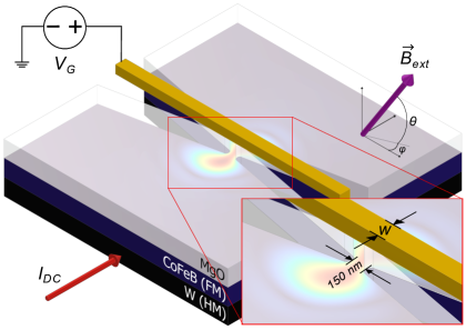
We simulated a W(5 nm)/CoFeB(1.7 nm)/MgO(2 nm) bow tie shaped bilayer with a nanoconstriction (NC) of 150 nm width, curvature radius of 50 nm, and opening angle of 22∘, as shown in Fig. 1. The geometry of the sample is taken from experiments in earlier work.Fulara et al. (2020) The in-plane current density and the Oersted field were sampled using the COMSOL multiphysics software COMSOL . The spin-polarized current density acting on the CoFeB layer due to the spin Hall effect was calculated by multiplying the in-plane current density at the W layer by a spin-Hall angle and the injected spin current polarized perpendicular to the local calculated current density.
The geometry of the SHNO, with a total volume of 409640961.7 nm3, was discretized into 102410241 cells and loaded into the GPU-accelerated micromagnetic simulator Mumax3 Vansteenkiste et al. (2014). The properties of the CoFeB layer were chosen as: exchange stiffness pJ/m, saturation magnetization kA/m, Gilbert damping constant , and gyromagnetic ratio GHz/T. An oblique magnetic field of 0.4T was applied at polar 60.5∘ and azimuthal 22.0∘ angles consistent with previous experiments.Fulara et al. (2020) To reduce artifacts due to spin wave reflections from the edge, periodic boundary conditions were used with absorbing borders, in the form of quadratically interpolated increased damping.
The VCMA was applied to a rectangular gated region by a voltage-dependent uniaxial perpendicular magnetic anisotropy (PMA) of the form,
| (1) |
where both the intrinsic and its linear gate voltage dependence were taken from experiments.Fulara et al. (2020) was swept from –80 V to +80 V to investigate a much wider range than studied previously. Although such high voltages are unlikely to be used, the corresponding change in can be realized at lower voltages using materials with higher VCMA coefficients.Choi et al. (2022)
For extraction of the linear response of the system, such as the dominant resonances and their damping, the FM layer was first relaxed, then excited with a short Gaussian pulse ( 10 ps) and allowed to decay back to equilibrium for 5 ns with a sampling rate of 10 ps. Then, the average magnetization in the center of the gate was converted to the frequency domain via a fast Fourier transform (FFT) and then fitted with a Lorentz distribution centered on the FMR frequency and with linewidth . From this fitting, the effective damping constant was calculated as
| (2) |
for all .Fulara et al. (2020) The average power was also estimated using the relation , where is the Fourier transform of the magnetization, to study all magnetodynamic modes.
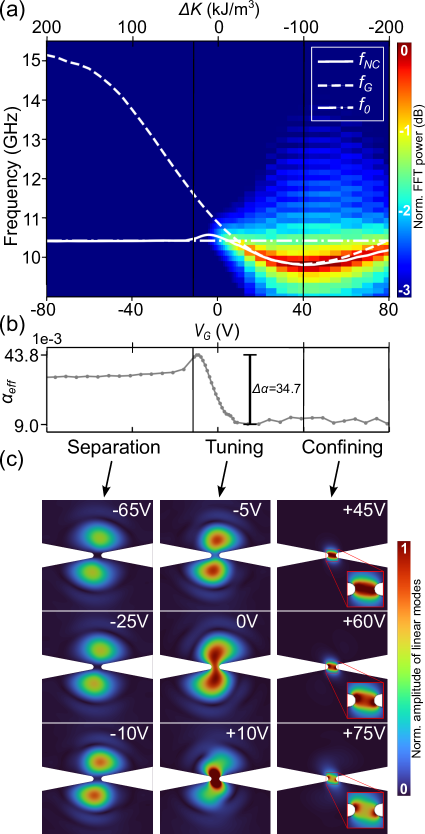
The power spectral density (PSD) map shown in Fig. 2(a) was constructed as a function of applied voltage and a gate of 96 nm. The nanoconstriction frequency, , and (Fig. 2(b)) were extracted for each case. Both quantities show a non-monotonic behavior and wide ranges of tunability, with a five-fold increase in damping within the -10 V to +10 V range and an accessible band of frequencies of approximately 800 MHz within the -5 V to +40 V range.
To investigate the origin of the nonmonotonic frequency behavior of the constriction mode, we simulated a FM layer with a geometry restricted to the gated region. The extracted frequency of this gate is plotted in Fig. 2(a), along with the intrinsic frequency of an ungated NC. From comparing the three frequency curves, we can conclude that the shape of emerges from the interplay of an intrinsic mode and a gated non-linear mode . In principle, we can switch between these two modes with voltage alone.
To gain more insight into the VCMA-mediated modulation of the effective damping and dynamics of the SHNO, we compared the spatially resolved mode profile amplitudes at for all . The mode profiles were constructed through a point-wise FFT, performed on magnetization snapshots sampled at 10 ps intervals, producing both the amplitude and phase maps of the oscillation modes. The mode amplitudes are shown in Fig. 2(c) where three voltage gating regimes can be identified based on the effect VCMA has on their features: a separation regime, a tuning regime, and a confining regime.
For strong negative voltages, the effective PMA under the gate becomes large and suppresses the excitation of localized modes in the gate region. Thus, the modes delocalize and separate into two coupled in-phase regions, as shown in the left column of Fig. 2(c). This separation regime spans from approximately –80 V to –10 V (or 200 kJ/m3 to 12.5 kJ/m3) and presents mostly flat and curves. Because the oscillations are driven out, the NC is driven mostly by the evanescent modes outside of it, which implies that the excited spin-wave volume increases, promoting radiative damping Slavin and Tiberkevich (2005); Demidov et al. (2012). The volume of this mode remains approximately the same and thus the damping is constant with voltage.
The tuning regime, with gate voltage around roughly –10 V to +40 V ( 12.5 kJ/m3 to –100 kJ/m3), is where we observe the largest tunabilities. From the middle column of Fig. 2(c), this regime shows the biggest change in excited mode volumes, which explains the 800 MHz tunability of frequency and five-fold increase in effective damping. These are due to the volume delocalization of the excited mode, which pushes emitted magnons into the non-gated region while preserving the mode’s core. The flattening of above +15V comes from the fact that the oscillations are limited to the gated region and we recover the intrinsic . Also, in this regime, the non-linear gated mode is close with the intrinsic mode of the system and thus drives the overall dynamics, reshaping . Such a range lends the device a lot of versatility as a microwave component, with the advantage of the low-power consumption a voltage source permits.
For high positive voltages between +40 V to +80 V ( –100 kJ/m3 to –200 kJ/m3), the local out-of-plane effective field angle is smoothly lowered with larger voltage (and smaller PMA). In this interval, the excited modes localized within the constriction, this regime also shows a minimum and a change in the sign of the derivative of . In this confining regime, the localized mode shifts between the bulk (where the oscillations occur mainly in the middle of the constriction) and the edge (where they occur mainly at the edges) Dvornik, Awad, and Åkerman (2018), as shown in the right column of Fig. 2(c).
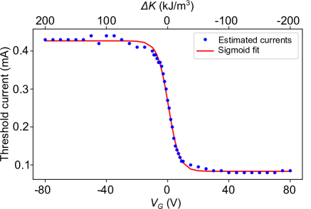
To determine the auto-oscillation threshold current, direct currents between 10 and 400 A were applied and analyzed for all . The auto-oscillation threshold is defined as the smallest current producing an exponentially growing amplitude. Fig. 3 shows the auto-oscillation threshold currents as a function of . The shape of the curve resembles a sigmoid logistic function, as shown in the fit, and it follows the behavior of the damping shown in Fig. 2(b), as expected. The sigmoid behavior draws similarities with an activation function in an artificial neural network, which invites exploration of possible technological avenues for arrays of SHNOs based on voltage-based synaptic activation. Very recent work seems to suggest a voltage-enabled synaptic potentiation and depression that could permit SHNO based neurons without external memory circuitry Choi et al. (2022).
Finally, to investigate the effect of the gate size on the modes, simulations and calculations of the frequency, damping, and power were repeated for a wide range of gate widths between 10 nm and 400 nm. In Fig. 4(a), where we show PSDs for six widths, a wider gate improves the tunability of the frequency by affecting (either by localization or delocalization) a larger area, thus increasing the concavity of the gated mode. For the three widest gates at the bottom, we can lower the voltages at which the gated mode is observable before the system switches back to its intrinsic mode. Furthermore, at w = 160 nm, we can see mode coexistence in the 0 V to –25 V interval.
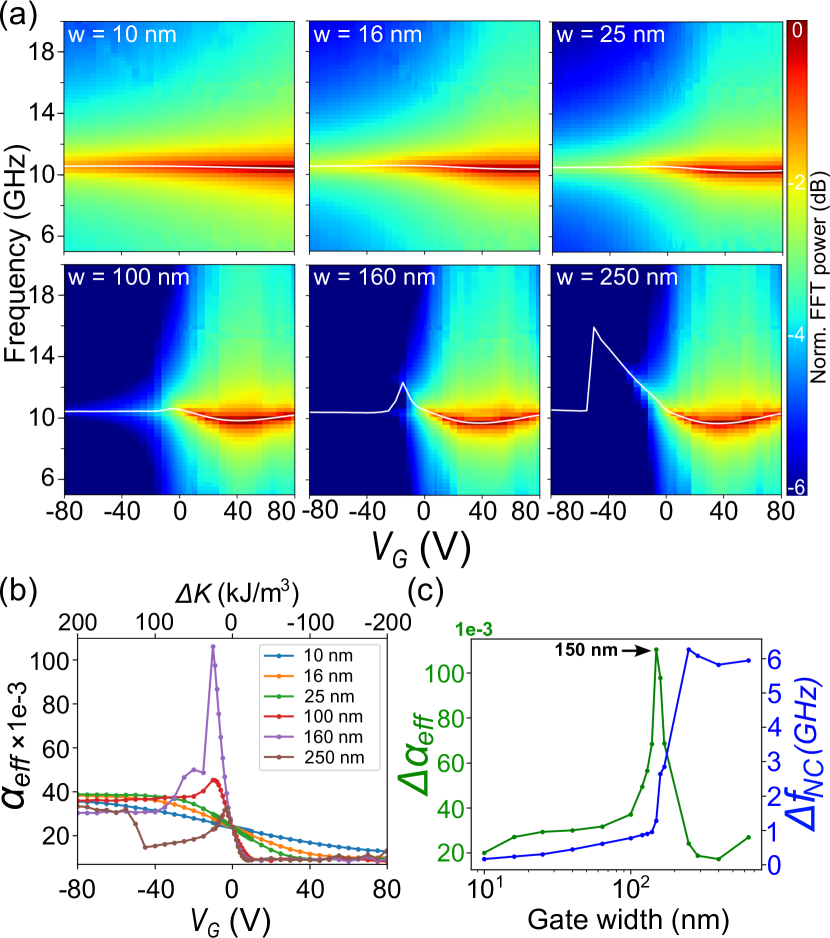
Fig. 4(b), shows that the width of the gate plays an important role in the radiative damping process. As the width of the gate increases, there is a gradual change in the shape of , with a sudden order of magnitude increase at 160 nm and a subsequent reduction at higher values. For this width value, increases with PMA up to a point, where PMA compensates the local demagnetization (at V), i.e. the sharp maximum is observed at the transition from in-plane to out-of-plane type of anisotropy.
The damping () and frequency () tunabilities are plotted in Fig. 4(c) as functions of the gate width. grows monotonically as the PMA is compensated in a bigger gated area. However, around 150 nm, there is a large increase in the slope of the curve before it saturates for wider gates. 150 nm corresponds to the constriction size and it is the width at which full compensation of the demagnetization field is achieved; wider gates lead to saturation of the compensation as the extending the area further does not affect compensation. There is also a sharp maximum in with a maximum at 150 nm gate width, where a matching between the width of the gate and the size of the mode’s core at the center of the nanoconstriction enhances the power transfer between the gated and non-gated regions and allows for a higher voltage-driven manipulation of the damping. For wider gates, the modes are driven out completely, and we have two uncoupled regions, with minimal damping tunability. The curves in Fig.4(c) could serve as a guide to design tailored devices for applications where a trade off between damping and frequency tunabilities might be important.
In conclusion, we find that the VCMA separates the local magnetodynamic properties of nanoconstriction-based SHNOs into three major regimes of mode confinement, tuning, and separation, with qualitatively different behavior. We find that the strongest tuning happens when the gate and nano-constriction have similar sizes, for which the damping can be varied by one order of magnitude and the frequency by several GHz. VCMA-oriented design paired with further developments in heterostructure fabrication techniques can hence pave the way towards more complex SHNO architectures for next generation unconventional spintronic computation platforms.
Acknowledgment
This work was supported by the Swedish Research Council (VR) and the Horizon 2020 research and innovation programme (ERC Advanced Grant No. 835068 ”TOPSPIN”).
Data Availability Statement
The code and output data that support the findings of this study are available from the corresponding author upon reasonable request.
References
- Liu et al. (2012) L. Liu, C.-F. Pai, D. C. Ralph, and R. A. Buhrman, “Magnetic oscillations driven by the spin hall effect in 3-terminal magnetic tunnel junction devices,” Phys. Rev. Lett. 109, 186602 (2012).
- Demidov et al. (2012) V. E. Demidov, S. Urazhdin, H. Ulrichs, V. Tiberkevich, A. Slavin, D. Baither, G. Schmitz, and S. O. Demokritov, “Magnetic nano-oscillator driven by pure spin current,” Nature Mater. 11, 1028–1031 (2012).
- Liu, Lim, and Urazhdin (2013) R. H. Liu, W. L. Lim, and S. Urazhdin, “Spectral Characteristics of the Microwave Emission by the Spin Hall Nano-Oscillator,” Phys. Rev. Lett. 110, 147601 (2013).
- Demidov et al. (2014a) V. E. Demidov, H. Ulrichs, S. V. Gurevich, S. O. Demokritov, V. S. Tiberkevich, A. N. Slavin, A. Zholud, and S. Urazhdin, “Synchronization of spin Hall nano-oscillators to external microwave signals,” Nat. Commun. 5, 3179 (2014a).
- Demidov et al. (2014b) V. E. Demidov, S. Urazhdin, A. Zholud, A. V. Sadovnikov, and S. O. Demokritov, “Nanoconstriction-based spin-Hall nano-oscillator,” Appl. Phys. Lett. 105, 172410 (2014b).
- Duan et al. (2014) Z. Duan, A. Smith, L. Yang, B. Youngblood, J. Lindner, V. E. Demidov, S. O. Demokritov, and I. N. Krivorotov, “Nanowire spin torque oscillator driven by spin orbit torques,” Nat. Commun. 5, 5616 (2014).
- Sato et al. (2019) N. Sato, K. Schultheiss, L. Körber, N. Puwenberg, T. Mühl, A. A. Awad, S. S. Arekapudi, O. Hellwig, J. Fassbender, and H. Schultheiss, “Domain Wall Based Spin-Hall Nano-Oscillators,” Physical Review Letters 123, 57204 (2019).
- Hirsch (1999) J. E. Hirsch, “Spin Hall Effect,” Phys. Rev. Lett. 83, 1834–1837 (1999).
- Hoffmann (2013) A. Hoffmann, “Spin Hall Effects in Metals,” IEEE Trans. Magn. 49, 5172–5193 (2013).
- Sinova et al. (2015) J. Sinova, S. O. Valenzuela, J. Wunderlich, C. H. Back, and T. Jungwirth, “Spin Hall effects,” Rev. Mod. Phys. 87, 1213–1260 (2015).
- Slonczewski (1996) J. C. Slonczewski, “Current-driven excitation of magnetic multilayers,” J. Magn. Magn. Mater. 159, L1–L7 (1996).
- Berger (1996) L. Berger, “Emission of spin waves by a magnetic multilayer traversed by a current,” Phys. Rev. B 54, 9353–9358 (1996).
- Ralph and Stiles (2008) D. C. Ralph and M. D. Stiles, “Spin transfer torques,” J. Magn. Magn. Mater. 320, 1190–1216 (2008).
- Awad et al. (2017) A. A. Awad, P. Dürrenfeld, A. Houshang, M. Dvornik, E. Iacocca, R. K. Dumas, and J. Åkerman, “Long-range mutual synchronization of spin Hall nano-oscillators,” Nature Physics 13, 292–299 (2017).
- Dürrenfeld et al. (2017) P. Dürrenfeld, A. a. Awad, A. Houshang, R. K. Dumas, and J. Åkerman, “A 20 nm spin Hall nano-oscillator,” Nanoscale 9, 1285–1291 (2017).
- Mazraati et al. (2016) H. Mazraati, S. Chung, A. Houshang, M. Dvornik, L. Piazza, F. Qejvanaj, S. Jiang, T. Q. Le, J. Weissenrieder, and J. Åkerman, “Low operational current spin hall nano-oscillators based on nife/w bilayers,” Applied Physics Letters 109, 242402 (2016).
- Zahedinejad et al. (2018) M. Zahedinejad, H. Mazraati, H. Fulara, J. Yue, S. Jiang, A. A. Awad, and J. Åkerman, “CMOS compatible W/CoFeB/MgO spin Hall nano-oscillators with wide frequency tunability,” Applied Physics Letters 112, 1–5 (2018).
- Mazraati et al. (2018) H. Mazraati, S. R. Etesami, S. A. H. Banuazizi, S. Chung, A. Houshang, A. A. Awad, M. Dvornik, and J. Åkerman, “Auto-oscillating spin-wave modes of constriction-based spin hall nano-oscillators in weak in-plane fields,” Physical Review Applied 10, 054017 (2018).
- Awad et al. (2020) A. A. Awad, A. Houshang, M. Zahedinejad, R. Khymyn, and J. Åkerman, “Width dependent auto-oscillating properties of constriction based spin Hall nano-oscillators,” Applied Physics Letters 116, 232401 (2020), arXiv:2003.07178 .
- Hache et al. (2019) T. Hache, T. Weinhold, K. Schultheiss, J. Stigloher, F. Vilsmeier, C. Back, S. S. Arekapudi, O. Hellwig, J. Fassbender, and H. Schultheiss, “Combined frequency and time domain measurements on injection-locked, constriction-based spin Hall nano-oscillators,” Applied Physics Letters 114 (2019).
- Zahedinejad et al. (2020) M. Zahedinejad, A. A. Awad, S. Muralidhar, R. Khymyn, H. Fulara, H. Mazraati, M. Dvornik, and J. Åkerman, “Two-dimensional mutually synchronized spin Hall nano-oscillator arrays for neuromorphic computing,” Nature Nanotechnology 15, 47 (2020).
- Yogendra et al. (2016) K. Yogendra, D. Fan, B. Jung, and K. Roy, “Magnetic pattern recognition using injection-locked spin-torque nano-oscillators,” IEEE Transactions on Electron Devices 63, 1674–1680 (2016).
- Romera et al. (2018) M. Romera, P. Talatchian, S. Tsunegi, F. A. Araujo, V. Cros, P. Bortolotti, J. Trastoy, K. Yakushiji, A. Fukushima, H. Kubota, S. Yuasa, M. Ernoult, D. Vodenicarevic, T. Hirtzlin, N. Locatelli, D. Querlioz, and J. Grollier, “Vowel recognition with four coupled spin-torque nano-oscillators,” Nature 563, 230 (2018).
- McGoldrick, Sun, and Liu (2022) B. C. McGoldrick, J. Z. Sun, and L. Liu, “Ising machine based on electrically coupled spin hall nano-oscillators,” Physical Review Applied 17, 014006 (2022).
- Albertsson et al. (2021) D. I. Albertsson, M. Zahedinejad, A. Houshang, R. Khymyn, J. Åkerman, and A. Rusu, “Ultrafast ising machines using spin torque nano-oscillators,” Applied Physics Letters 118, 112404 (2021).
- Houshang et al. (2022) A. Houshang, M. Zahedinejad, S. Muralidhar, J. Chȩciński, R. Khymyn, M. Rajabali, H. Fulara, A. A. Awad, M. Dvornik, and J. Åkerman, “Phase-binarized spin hall nano-oscillator arrays: Towards spin hall ising machines,” Phys. Rev. Applied 17, 014003 (2022).
- Muralidhar et al. (2022) S. Muralidhar, A. Houshang, A. Alemán, R. Khymyn, A. A. Awad, and J. Åkerman, “Optothermal control of spin hall nano-oscillators,” Applied Physics Letters 120, 262401 (2022), https://doi.org/10.1063/5.0086758 .
- Liu et al. (2017) R. H. Liu, L. Chen, S. Urazhdin, and Y. W. Du, “Controlling the spectral characteristics of a spin-current auto-oscillator with an electric field,” Phys. Rev. Applied 8, 021001 (2017).
- Fulara et al. (2020) H. Fulara, M. Zahedinejad, R. Khymyn, M. Dvornik, S. Fukami, S. Kanai, H. Ohno, and J. Åkerman, “Giant voltage-controlled modulation of spin hall nano-oscillator damping,” Nature Communications 11, 4006 (2020).
- Zahedinejad et al. (2022) M. Zahedinejad, H. Fulara, R. Khymyn, A. Houshang, M. Dvornik, S. Fukami, S. Kanai, H. Ohno, and J. Åkerman, “Memristive control of mutual spin hall nano-oscillator synchronization for neuromorphic computing,” Nat Mater. 21, 81–87 (2022), https://doi.org/10.1038/s41563-021-01153-6 .
- Choi et al. (2022) J.-G. Choi, J. Park, M.-G. Kang, D. Kim, J.-S. Rieh, K.-J. Lee, K.-J. Kim, and B.-G. Park, “Voltage-driven gigahertz frequency tuning of spin hall nano-oscillators,” Nature Communications 13, 3783 (2022).
- (32) COMSOL, “Comsol multiphysics software,” .
- Vansteenkiste et al. (2014) A. Vansteenkiste, J. Leliaert, M. Dvornik, M. Helsen, F. Garcia Sanchez, and B. Van Waeyenberge, “The design and verification of MuMax3,” AIP Adv. 4, 107133 (2014).
- Slavin and Tiberkevich (2005) A. Slavin and V. Tiberkevich, “Spin Wave Mode Excited by Spin-Polarized Current in a Magnetic Nanocontact is a Standing Self-Localized Wave Bullet,” Phys. Rev. Lett. 95, 237201 (2005).
- Dvornik, Awad, and Åkerman (2018) M. Dvornik, A. A. Awad, and J. Åkerman, “Origin of magnetization auto-oscillations in constriction-based spin hall nano-oscillators,” Phys. Rev. Applied 9, 014017 (2018).