High-field and high-temperature magnetoresistance reveals the superconducting behaviour of the stacking faults in multilayer graphene
Abstract
In spite of 40 years of experimental studies and several theoretical proposals, an overall interpretation of the complex behavior of the magnetoresistance (MR) of multilayer graphene, i.e. graphite, at high fields (T) and in a broad temperature range is still lacking. Part of the complexity is due to the contribution of stacking faults (SFs), which most of thick enough multilayer graphene samples have. We propose a procedure that allows us to extract the SF contribution to the MR we have measured at 0.48 K 250 K and 0 T 65 T. We found that the MR behavior of part of the SFs is similar to that of granular superconductors with a superconducting critical temperature 350 K, in agreement with recent publications. The measurements were done on a multilayer graphene TEM lamella, contacting the edges of the two-dimensional SFs.
I Introduction
The recent discovery of superconductivity in twisted bilayer graphene cao18 ; yan19 , a stacking fault in itself, in trilayer graphene moiré superlattice che19 as well as in rhombohedral stacking order zho21 at K supports the assumption that the origin of the “hidden superconductivity” reported in several bulk and mesoscopic graphite samples in the last 50 years ant74 ; ant75 ; yakovjltp00 ; esq08 ; esqpip , is related to the existence of two-dimensional stacking faults (SFs). Because these SFs are embedded in a multilayer-graphene matrix with a Bernal (2H) or rhombohedral (3R) stacking order, they can play a main role in the measured transport properties. Previous studies demonstrated that SFs, like twisted graphene layers, are common in well-ordered graphite samples kuw90 ; mil10 ; flo13 . Therefore, flat bands regions are expected to be found in bulk and mesoscopic graphite samples at certain SFs, where superconductivity at low and high temperatures is predicted kop13 ; mun13 ; hei16 ; vol18 ; cea19 .
The tuning of superconductivity in mesoscopic bi- and trilayers graphene samples through the fabrication of regions with well-defined twist angle, added to the possibility of contacting directly the superconducting region, are clear advantages with respect to experimental studies in bulk or mesoscopic graphite samples. Although the existence of a large number of SFs can be recognized by Scanning Transmission Electron Microscopy (STEM) and X-rays Diffraction (XRD) analysis Esquinazi2017 , the twist angle distribution remains largely unknown in thick multilayer graphene samples. However, there are some advantages in the study of the behavior of the SFs in well-ordered multilayer graphene or graphite samples. One of them is that SFs of very large areas (several 100’s of m2) with high degree of lattice order can be found well shielded from environmental influence. Another advantage is that thick enough samples can have up to of the 3R stacking, in addition to the main 2H-type stacking kelly ; wu22 . The SFs between untwisted 2H and 3R crystalline regions are expected to have high superconducting temperatures kop13 ; mun13 ; hei16 ; vol18 . This kind of SF has not yet been produced in a controllable way. On the other hand, if superconductivity is located at certain regions of such large SF areas, we expect to have granular and not homogeneous superconductivity, i.e. Josephson coupled superconducting regions of several tens of m2 each. Our research covers the study of the low and very high field behavior of the magnetoresistance (MR) of the SFs in multilayer graphene extracted from the measured MR with the help of a procedure we developed. The results clarify several open questions on the interpretation of the MR of graphite and indicate the existence of superconducting regions with an upper critical temperature of K.
II Methods and sample
We have prepared a multilayer graphene TEM lamella of dimensions m m m, with the width in the -axis direction, obtained from a highly oriented pyrolytic graphite (HOPG) bulk sample using a similar procedure as in bal13 , and investigated the transport properties at low- and high-fields (applied parallel to the -axis) in a broad temperature range. The lamella was fixed on a substrate combining electron beam lithography with SiNx deposition covering part of the sample surface. Afterwards, the lamella was inductively etched with a plasma reactive ion etching system (ICP-RIE) to take out the disordered graphite layer formed during the milling process. Four electrodes were prepared with electron beam lithography and depositing Cr/Au, see the sample optical image in the inset of Fig.2(b). The sample electrical resistance at 300 K was 7.44 . As we show below, such a TEM lamella with the graphite axis parallel to the substrate provides the best way to get the SFs contribution to the total electrical resistance by contacting their edges. Considering the width (in the axis direction) of the sample and the corresponding STEM images in samples from the same batch, see Refs. bal13 ; Esquinazi2017 , the number of SFs is significant. Therefore, our electrical voltage contacts pick up the response of several of them; the current input is distributed through all SFs. In this way, we expect to get the superconducting response of the SFs with the highest critical temperature.
For measurements at 2 K 300 K and DC magnetic fields T we used a 4He cryostat, prior to the high field pulsed measurements. These last measurements were performed at the National High Magnetic Field Laboratory’s Pulsed Field Facility (NHMFL-PFF) at Los Alamos National Laboratory (LANL) Jaime2006 . The measurements were done in a cryostat with a temperature range = 0.45 K to 250 K, equipped with a 65 T multi-shot magnet, powered by a 32 mF, 4 MJ capacitor bank with a pulse duration of ms Swenson2004 ; Nguyen2016 . Most of the experiments were performed with pulses of 60 T. An alternating current of 12 A amplitude was applied to the sample at a frequency of 50.5 kHz. The voltage was measured with a 20 MHz sampling rate. The field was always normal to the graphene planes and the SFs.
III Results and discussion
Electrical transport measurements under high magnetic fields (T) performed in bulk and millimeter long multilayer graphene samples were reported in the last 40 years Tanuma1981 ; Yaguchi1998 ; Fauque2013 ; Akiba2015 . The observed behavior of the MR of those samples is complex and non-monotonous in field. Several interpretations were proposed, namely: fluctuations of charge density waves Yoshioka1981 ; Timp1983 , magnetic freeze-out of carriers Brandt1974 , 3D quantum Hall effect through the appearance of chiral surface states Fauque2013 ; Bernevig2007 , the emergence of an excitonic BCS-like state Akiba2015 , the appearance of an insulating surface states that carry no charge or spin within the planes Arnold2017 , magnetic catalysis scenario GORBAR-02 ; KHV-01 ; DETAR-16 , to cite a few of them. However, none of those studies considered the parallel contributions of at least two subsystems in graphite gar12 ; zor17 , i.e., the MR of the SFs and the one from the graphite matrix with mostly Bernal stacking order.
The incorrect interpretations of the transport, as well as the magnetization properties of graphite found in several early reports, relied on the assumption of electrically homogeneous samples. The lack of TEM or STEM characterization with the electron beam parallel to the graphene planes necessary to get an evidence of the existence of SFs, impeded in the past a timely development of the physics of graphite and of its SFs. One prominent example is the common, incorrect assumption that graphite is a semimetal with a finite Fermi surface at low temperatures. Systematic transport studies as a function of the thickness of graphite samples proved, however, that the SFs substantially contribute to the electrical transport and are at the origin of Shubnikov-de Haas (SdH) (or de Haas-van Alphen in the magnetization) quantum oscillations zor18 . The vanishing of the SdH oscillations amplitude the smaller the thickness of the graphite samples, maintaining their high structural ordering, was recognized already at the beginning of 2000 without providing a clear interpretation of this behavior oha00 ; oha01 . The change in the temperature and field dependence of the electrical transport as a function of the graphite sample thickness already indicated that the metalliclike behavior vanishes when the thickness of the sample is smaller than the average distance between the SFs bar08 , which for the HOPG sample we used in this study means a length in the axis direction of less than nm. From different characterizations gar12 ; esq14 ; zor17 ; Barzola2019 ; reg21 we know nowadays that the intrinsic properties of ideal graphite, i.e. without SFs, are compatible with those of a narrow band semiconductor, not a semimetal and a finite Fermi surface does not exist at low temperatures. Stacking faults with superconducting behavior can be also found in mesoscopic and bulk samples, see Esquinazi2017 and Refs. therein.
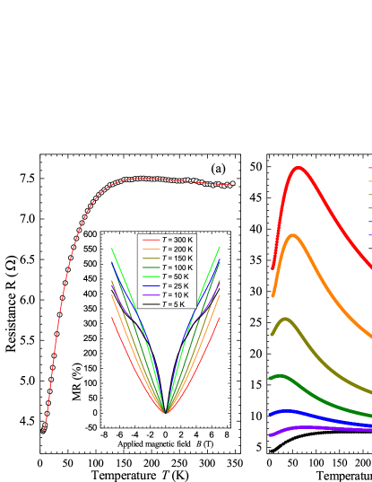
The temperature dependence of the resistance at is shown in Fig.1(a). The resistance increases with temperature to K, decreasing at higher . This is one possible behavior of for bulk and thick flakes of graphite reported in the literature gar12 ; zor17 . The red line in Fig.1 (a) is a fit to a parallel resistance model given by the contribution of the SFs and of the main ideal graphite matrix gar12 :
| (1) |
where is the total sample resistance (see Refs. gar12 ; zor17 for the full expression). has an increasing with temperature contribution given by an exponential function of the form . The thermal activation energy meV is obtained from the fit. We note that this temperature dependent behavior is expected for granular superconductors according to Refs. sha83 ; lan67 ; mcc70 ; str07 .
The narrow-gap semiconducting contribution of the 2H matrix can be approximated as with an energy gap meV obtained from the fit. All fit parameters are similar to those reported in the literature zor17 ; gar12 , emphasizing that the measured sample is representative. Due to its small amount, we neglect the semiconducting parallel contribution of the 3R matrix to the total . We note that the excellent fits of obtained for graphite samples of different thickness using the parallel resistance model and those exponential terms is not obtained by replacing them with or other dependencies found in the literature zor17 .
The inset in Fig.1(a) shows the magnetoresistance defined as MR measured at different constant temperatures with magnetic fields between T. At K, SdH oscillations are detected with the main period in of 0.21 T-1 in agreement with the literature. From this period we estimate a 2D carrier density cm-2 at certain SFs that originate the SdH oscillations zor18 . Fig.1(b) shows the dependence of the electrical resistance of the lamella at different magnetic fields. The sample shows the typical re-entrant metallic behavior at T and K reported for bulk graphite samples yakovprl03 .
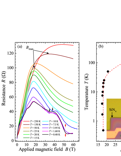
Fig.2(a) shows the absolute value of the electrical resistance of the lamella vs. magnetic field at different temperatures. The electronic transitions () and () are clearly recognized at K in the field range 30 T 55 T. Fig.2(b) shows the dependence of the field at which the MR shows a maximum, see Fig.2(a). We found that remains independent at K. Above this temperature increases. This behavior is in very good agreement with that reported several times in the last 40 years Tanuma1981 ; Yaguchi1998 ; Iye1982 ; Ochimizu1992 ; Akiba2015 ; Arnold2017 . In particular, the behavior of was explained on the basis of the magnetic catalysis model KHV-01 . From all the measured data we conclude that this TEM lamella shows all the characteristics of the electrical resistance and magnetoresistance of bulk graphite samples. We provide below an interpretation of the observed behavior.
We will extract first the SF resistance from the measured data. For that we rewrite Eq.(1) at a constant temperature as:
| (2) |
The MR of the 2H contribution can be described by the two-band model (TBM) appropriate for semiconductors and derived under the Boltzmann-Drude quasi-classical diffusive approach kelly . As emphasized above, the transport properties of ideal graphite (without SFs) match the ones of a narrow-band gap semiconductor. Therefore, we approximate the field-dependent resistance related to the semiconducting 2H-contribution as:
| (3) |
where we have assumed equal mobility for both electrons and holes (), and is the relative charge imbalance between electron and hole carrier densities.
The simplified expression of Eq.(3) has only two adjustable fitting parameters: the average mobility and the relative charge imbalance ; is a fixed parameter obtained from the fit in Fig.1(a). Eq.(3) provides two key features of the MR of the semiconducting contribution, namely, the field dependence at low fields and its saturation at high enough fields.
Replacing Eq.(3) in Eq.(2), we obtain plotted in Fig.3(a). The results indicate that at K, because the semiconducting contribution becomes negligible, i.e. . We further note that shows a maximum at T, which does not depend significantly on within error, see Fig.3(b). These results indicate that the temperature shift of in the MR, see Fig.2(b), is an artifact caused by the growing influence at K of the semiconducting contribution in parallel to the SFs one. Regarding the parameters used, the charge imbalance between electrons and holes was considered constant , and the obtained mobility decreases with temperature (see inset in Fig.3(b)), in qualitative agreement with the behavior found in the literature Pendrys1980 ; esq12 .
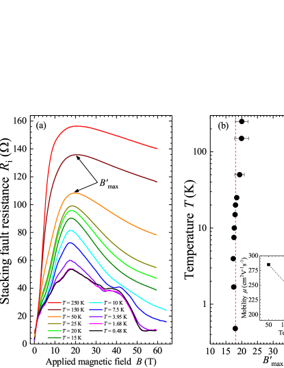
The MR of the SF () plotted in Fig.3(a), resembles the one observed in granular superconductors, like granular Al in a Ge matrix or InO films Shapira1983 ; Gerber1997 ; Gantmakher1996 . In particular, it shows a linear increase with field at low fields and decreases at fields above a certain field. The explanation for the linear increase with field discussed in the literature is based on the influence of the field in the Josephson coupling between superconducting regions or in our case 2D regions (or ‘grains”) at some SFs. The higher the field, the larger is the number of uncoupled superconducting regions and the resistance increases linearly. After a maximum number of independent regions is reached at , a higher field increases the density of states inside those regions, increasing the probability of having Cooper pairs and the resistance starts to decrease with field. In this field range, the intragrain superconducting fluctuations affect the intergrain conductivity reducing the total resistance. This appears to be a general behavior in granular superconductors, see Fig. 7 in Ref. Barzola2019 and Refs. therein. We expect therefore that the field at which starts to saturate can be considered as a critical field . This appears to be the case at a field T at K, see Fig.3(a). However, we expect that decreases with temperature, which is not clearly observed in of Fig.3(a) at K. The absence of a clear saturation at high temperatures and fields could be due to superconducting fluctuations, which in granular superconductors are expected to persist up to very high fields and temperatures Gantmakher1996 .
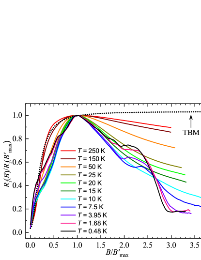
Fig.4 shows the normalized vs the normalized magnetic field at different temperatures. We note that the higher the temperature the smaller is the decrease of the resistance with field at . This is expected because the number and/or size of the superconducting regions inside the SFs should in this case decrease. Therefore, at the highest critical temperature of the superconducting grains, there should not be a decrease with field of . At we expect a MR behavior similar to the semiconducting matrix, approximately given by the TBM, see Fig.4.
Together with the similarities of our results to those of granular superconductors, let us emphasize here why we expect to have granular superconductivity at certain SFs and not a homogeneous state. Granular superconductivity occurs because the flat bands formed at the 2D SFs are not homogeneous in areas more than a few tens of micrometer square. This is obvious if we take into account the STEM evidence about the order or disorder that usual graphite samples have. Not only the perfection of a 2D SFs in the corresponding plane is an issue but also, e.g., the flat bands can be affected by the number of ideal graphene layers on both side of the interface. In addition, the graphene layers are not ideal over the sample, but have boundaries that restrict the homogeneous regions. This is a fact that is simple to recognize from STEM images taken at energies keV. The granular nature was already shown to be highly likely in several reports, as for example bal13 ; schcar ; bal15 . At low enough temperatures and currents in the nA region, curves indicate indeed a Josephson behavior and zero resistance within error bal13 . Even the reported transition in twisted bilayer graphene mesoscopic samples does not appear to behave as a homogeneous but as a granular superconductor, as a direct, quantitative comparison between those results and the ones obtained in graphite TEM lamellae indicates esq19 .
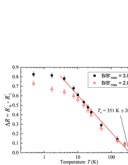
The proposed interpretation of the MR of the SFs in terms of Josephson-coupled superconducting regions at certain interfaces or SFs, implies that at a fixed field the temperature dependence of the resistance should be compatible with the one expected for 2D granular superconductors. An analytical expression for the resistance of this 2D system within the effective medium approximation has been obtained in str07 . In particular, at fields near the critical field or at high enough temperatures the resistance between superconducting grains reaches a critical resistance , which self-consistent solution (see Fig.3 in str07 ) follows nearly a at , independently of the value of the assumed charging energy. We compare qualitatively this prediction with the difference between the normalized resistance in the normal state and the normalized SF resistance () from Fig.4, at and 3. The difference follows a at high enough temperatures and a critical temperature K is obtained by extrapolation to , see Fig.5. Interestingly, this agrees with the one suggested by different transport, magnetization Precker2016 ; lay22 ; rou22 and magnetic force microscopy sti18 ; ari22 measurements in different, well ordered natural graphite samples. At lower , the behavior of is affected by the transition to the normal state or by the electronic transitions, see Fig.4, preventing a comparison with the predicted in the whole temperature range.
IV Conclusion
The MR of a multilayer graphene TEM lamella shows a temperature-dependent maximum at , which increases with temperature in agreement with earlier measurements of large graphite samples. Assuming that the MR is given by the parallel contribution of a semiconducting graphite matrix and of the stacking faults, we were able to extract the MR of this last in a broad temperature and magnetic field ranges. Our results indicate that the observed temperature dependence of is an artifact due to the increasing contribution of the semiconducting graphite matrix with temperature. The extracted stacking fault MR shows several features compatible with those found in granular superconductors. The extrapolated maximum superconducting critical temperature of K for the superconducting regions at the stacking faults is in agreement with recent reports.
Acknowledgments: The authors thanks Zhipeng Zhang for the deposition of SiNx, and Marius Grundmann for giving access the to ICP-RIE. C.E.P. gratefully acknowledges the support provided by the Brazilian National Council for the Improvement of Higher Education (CAPES) under 99999.013188/2013-05. MJ and MKC acknowledge support by the US DOE Basic Energy Science project “Science at 100T”. The studies were partially supported by the DAAD Nr. 57207627, by the DFG under ES 86/29-1 and 31047526 (SFB 762) and the European Regional Development Fund Grant Nr.: 231301388. A portion of this work was performed at the National High Magnetic Field Laboratory, which is supported by the NSF Cooperative Agreement No. DMR-1644779, the US DOE and the State of Florida.
Data Archival: All the data included in the figures will be available at https://speicherwolke.uni-leipzig.de/index.php/s/X3TPRBwHYKrJM54 and on request from the corresponding author (PDE).
1ceprecker@gmail.com; Current address: AIMEN Technology Centre, Smart Systems and Smart Manufacturing-Artificial Intelligence and Data Analytics Laboratory, PI. Cataboi, 36418 Pontevedra, Spain
2Current address: Goldschmidtstrasse 21, 04103 Leipzig, Germany
References
- (1) Y. Cao, V. Fatemi, S. Fang, K. Watanabe, T. Taniguchi, E. Kaxiras, P. Jarillo-Herrero, Unconventional superconductivity in magic-angle graphene superlattices, Nature 556 (7699) (2018) 43–50. doi:10.1038/nature26160.
- (2) M. Yankowitz, S. Chen, H. Polshyn, Y. Zhang, K. Watanabe, T. Taniguchi, D. Graf, A. F. Young, C. R. Dean, Tuning superconductivity in twisted bilayer graphene, Science 363 (6431) (2019) 1059–1064. doi:10.1126/science.aav1910.
- (3) G. Chen, A. L. Sharpe, P. Gallagher, I. T. Rosen, E. J. Fox, L. Jiang, B. Lyu, H. Li, K. Watanabe, T. Taniguchi, J. Jung, Z. Shi, D. Goldhaber-Gordon, Y. Zhang, F. Wang, Signatures of tunable superconductivity in a trilayer graphene moiré superlattice, Nature 572 (2019) 215–219. doi:10.1038/s41586-019-1393-y.
- (4) H. Zhou, T. Xie, T. Taniguchi, K. Watanabe, A. F. Young, Superconductivity in rhombohedral trilayer graphene, Nature 598 (2021) 434–438. doi:10.1038/s41586-021-03926-0.
- (5) K. Antonowicz, Possible superconductivity at room temperature, Nature 247 (1974) 358–360. doi:https://doi.org/10.1038/247358a0.
- (6) K. Antonowicz, The effect of microwaves on dc current in an Al-Carbon-Al sandwich, phys. stat. sol. (a) 28 (1975) 497–502. doi:https://doi.org/10.1002/pssa.2210280214.
- (7) Y. Kopelevich, P. Esquinazi, J. Torres, S. Moehlecke, Ferromagnetic- and superconducting-like behavior of graphite, J. Low Temp. Phys. 119 (2000) 691–702. doi:https://doi.org/10.1023/A:1004637814008.
- (8) P. Esquinazi, N. García, J. Barzola-Quiquia, P. Rödiger, K. Schindler, J.-L. Yao, M. Ziese, Indications for intrinsic superconductivity in highly oriented pyrolytic graphite, Phys. Rev. B 78 (2008) 134516. doi:https://doi.org/10.1103/PhysRevB.78.134516.
- (9) P. Esquinazi, Graphite and its hidden superconductivity, Papers in Physics 5 (2013) 050007. doi:https://doi.org/10.4279/pip.050007.
- (10) M. Kuwabara, D. R. Clarke, A. A. Smith, Anomalous superperiodicity in scanning tunnelling microscope images in graphite, Appl. Phys. Lett. 56 (1990) 2396. doi:https://doi.org/10.1063/1.102906.
- (11) D. L. Miller, K. D. Kubista, G. M. Rutter, M. Ruan, W. A. de Heer, P. N. First, J. A. Stroscio, Structural analysis of multilayer graphene via atomic moiré interferometry, Phys. Rev. B 81 (2010) 125427. doi:https://doi.org/10.1103/PhysRevB.81.125427.
- (12) M. Flores, E. Cisternas, J. Correa, P. Vargas, Moiré patterns on stm images of graphite induced by rotations of surface and subsurface layer, Chemical Physics 423 (2013) 49–54. doi:https://doi.org/10.1016/j.chemphys.2013.06.022.
- (13) N. B. Kopnin, M. Ijäs, A. Harju, T. T. Heikkilä, High-temperature surface superconductivity in rhombohedral graphite, Phys. Rev. B 87 (2013) 140503. doi:10.1103/PhysRevB.87.140503.
- (14) W. A. Muñoz, L. Covaci, F. Peeters, Tight-binding description of intrinsic superconducting correlations in multilayer graphene, Phys. Rev. B 87 (2013) 134509. doi:10.1103/PhysRevB.87.134509.
- (15) T. Heikkilä, G. E. Volovik, Flat bands as a route to high-temperature superconductivity in graphite, P. Esquinazi (ed.), Springer International Publishing AG Switzerland, 2016, pp. 123–144. doi:https://doi.org/10.1007/978-3-319-39355-1-6.
- (16) G. E. Volovik, Graphite, graphene, and the flat band superconductivity, JETP Letters 107 (2018) 516–517. doi:https://doi.org/10.1134/S0021364018080052.
- (17) T. Cea, N. R. Walet, F. Guinea, Twists and the electronic structure of graphitic materials, Nano Letters 19 (12) (2019) 8683–8689. doi:10.1021/acs.nanolett.9b03335.
- (18) P. D. Esquinazi, C. E. Precker, M. Stiller, T. R. S. Cordeiro, J. Barzola-Quiquia, A. Setzer, W. Böhlmann, Evidence for room temperature superconductivity at graphite interfaces, Quantum Studies: Mathematics and Foundations 5 (1) (2017) 41–53. arXiv:1709.00259, doi:10.1007/s40509-017-0131-0.
- (19) B. T. Kelly, Physics of Graphite, London: Applied Science Publishers, 1981.
- (20) H. Wu, J. Song, S. Wang, J. Wen, A. Gu, Y. Dai, W. Li, H. Zhang, F. S. Boi, Coexistence of crystalline rhombohedral stacking and hexagonal moiré superlattices in exfoliated highly oriented pyrolytic graphite, Materials Today Communications (2022) 104152. doi:https://doi.org/10.1016/j.mtcomm.2022.104152.
- (21) A. Ballestar, J. Barzola-Quiquia, T. Scheike, P. Esquinazi, Evidence of Josephson-coupled superconducting regions at the interfaces of highly oriented pyrolytic graphite, New J. Phys. 15 (2013) 023024. doi:https://doi.org/10.1088/1367-2630/15/2/023024.
- (22) M. Jaime, A. Lacerda, Y. Takano, G. S. Boebinger, The national high magnetic field laboratory, Journal of Physics: Conference Series 51 (1) (2006) 643–646. doi:10.1088/1742-6596/51/1/148.
- (23) C. Swenson, W. Marshall, E. Miller, K. Pickard, A. Gavrilin, K. Han, H. Schneider-Muntau, Pulse Magnet Development Program at NHMFL, IEEE Transactions on Appiled Superconductivity 14 (2) (2004) 1233–1236. doi:10.1109/TASC.2004.830538.
- (24) D. N. Nguyen, J. Michel, C. H. Mielke, Status and Development of Pulsed Magnets at the NHMFL Pulsed Field Facility, IEEE Transactions on Applied Superconductivity 26 (4) (2016) 1–5. doi:10.1109/TASC.2016.2515982.
- (25) S. Tanuma, R. Inada, A. Furukawa, O. Takahashi, Y. Iye, Y. Onuki, Electrical Properties of Layered Materials at High Magnetic Fields, in: S. Chikazumi, N. Miura (Eds.), Physics in High Magnetic Fields, 1st Edition, Vol. 24 of Springer Series in Solid-State Sciences, Springer, Berlin, 1981, pp. 316–319. doi:10.1007/978-3-642-81595-9.
- (26) H. Yaguchi, J. Singleton, Destruction of the Field-Induced Density-Wave State in Graphite by Large Magnetic Fields, Physical Review Letters 81 (23) (1998) 5193–5196. doi:10.1103/PhysRevLett.81.5193.
- (27) B. Fauqué, D. LeBoeuf, B. Vignolle, M. Nardone, C. Proust, K. Behnia, Two Phase Transitions Induced by a Magnetic Field in Graphite, Physical Review Letters 110 (26) (2013) 266601. arXiv:1303.4074, doi:10.1103/PhysRevLett.110.266601.
- (28) K. Akiba, A. Miyake, H. Yaguchi, A. Matsuo, K. Kindo, M. Tokunaga, Possible Excitonic Phase of Graphite in the Quantum Limit State, Journal of the Physical Society of Japan 84 (5) (2015) 054709. arXiv:1503.04414, doi:10.7566/JPSJ.84.054709.
- (29) D. Yoshioka, H. Fukuyama, Electronic Phase Transition of Graphite in a Strong Magnetic Field, Journal of the Physical Society of Japan 50 (3) (1981) 725–726. doi:10.1143/JPSJ.50.725.
- (30) G. Timp, P. D. Dresselhaus, T. C. Chieu, G. Dresselhaus, Y. Iye, Anomalous magnetoresistance of graphite at high magnetic fields, Physical Review B 28 (12) (1983) 7393–7396. doi:10.1103/PhysRevB.28.7393.
- (31) N. B. Brandt, G. A. Kapustin, V. G. Karavaev, A. S. Kotosonov, E. A. Svistova, Investigation of the galvanomagnetic properties of graphite in magnetic fields up to 500~kOe at low temperatures, Sov. Phys.-JETP 40 (3) (1974) 564–569. doi:http://jetp.ac.ru/cgi-bin/dn/e-040-03-0564.pdf.
- (32) B. A. Bernevig, T. L. Hughes, S. Raghu, D. P. Arovas, Theory of the three-dimensional quantum Hall effect in graphite, Physical Review Letters 99 (14) (2007) 5–8. arXiv:0701436, doi:10.1103/PhysRevLett.99.146804.
- (33) F. Arnold, A. Isidori, E. Kampert, B. Yager, M. Eschrig, J. Saunders, Charge Density Waves in Graphite: Towards the Magnetic Ultraquantum Limit, Physical Review Letters 119 (13) (2017) 136601. doi:10.1103/PhysRevLett.119.136601.
- (34) E. Gorbar, V. Gusynin, V. Miransky, I. Shovkovy, Magnetic field driven metal-insulator phase transition in planar systems, Phys. Rev. B 66 (2002) 045108. doi:10.1103/PhysRevB.66.045108.
- (35) D. Khveshchenko, Magnetic-field-induced insulating behavior in highly oriented pyrolitic graphite, Phys. Rev. Lett. 87 (2001) 206401. doi:10.1103/PhysRevLett.87.206401.
- (36) C. DeTar, C. Winterowd, S. Zafeiropoulos, Magnetic catalysis in graphene effective field theory, Phys. Rev. Lett. 117 (2016) 266802. doi:10.1103/PhysRevLett.117.266802.
- (37) N. García, P. Esquinazi, J. Barzola-Quiquia, S. Dusari, Evidence for semiconducting behavior with a narrow band gap of Bernal graphite, New Journal of Physics 14 (5) (2012) 053015. doi:https://doi.org/10.1088/1367-2630/14/5/053015.
- (38) M. Zoraghi, J. Barzola-Quiquia, M. Stiller, A. Setzer, P. Esquinazi, G. Kloess, T. Muenster, T. Lühmann, I. Estrela-Lopis, Influence of rhombohedral stacking order in the electrical resistance of bulk and mesoscopic graphite, Phys. Rev. B 95 (2017) 045308. doi:10.1103/PhysRevB.95.045308.
- (39) M. Zoraghi, J. Barzola-Quiquia, M. Stiller, P. D. Esquinazi, I. Estrela-Lopis, Influence of interfaces on the transport properties of graphite revealed by nanometer thickness reduction, Carbon 139 (2018) 1074 – 1084. doi:https://doi.org/10.1016/j.carbon.2018.07.070.
- (40) Y. Ohashi, T. Hironaka, T. Kubo, K. Shiiki, Magnetoresistance effect of thin films made of single graphite crystals, TANSO 195 (2000) 410–413.
- (41) Y. Ohashi, K. Yamamoto, T. Kubo, Shubnikov - de Haas effect of very thin graphite crystals, Carbon’01, An International Conference on Carbon, Lexington, KY, United States, July 14-19, Publisher: The American Carbon Society, available at www.acs.omnibooksonline.com (2001) 568–570.
- (42) J. Barzola-Quiquia, J.-L. Yao, P. Rödiger, K. Schindler, P. Esquinazi, Sample size effects on the transport properties of mesoscopic graphite samples, phys. stat. sol. (a) 205 (2008) 2924–2933.
- (43) P. Esquinazi, J. Krüger, J. Barzola-Quiquia, R. Schönemann, T. Hermannsdörfer, N. García, On the low-field Hall coefficient of graphite, AIP Advances 4 (2014) 117121.
- (44) J. Barzola-Quiquia, P. D. Esquinazi, C. E. Precker, M. Stiller, M. Zoraghi, T. Förster, T. Herrmannsdörfer, W. A. Coniglio, High-field magnetoresistance of graphite revised, Physical Review Materials 3 (5) (2019) 054603. doi:10.1103/PhysRevMaterials.3.054603.
- (45) R. Ariskina, M. Schnedler, P. D. Esquinazi, A. Champi, M. Stiller, W. Hergert, R. E. Dunin-Borkowski, P. Ebert, T. Venus, I. Estrela-Lopis, Influence of surface band bending on a narrow band gap semiconductor: Tunneling atomic force studies of graphite with bernal and rhombohedral stacking orders, Phys. Rev. Materials 5 (2021) 044601. doi:10.1103/PhysRevMaterials.5.044601.
- (46) Y. Shapira, G. Deutscher, Semiconductor-superconductor transition in granular al-ge, Phys. Rev. B 27 (1983) 4463–4466. doi:10.1103/PhysRevB.27.4463.
- (47) J. S. Langer, V. Ambegaokar, Intrinsic resistive transition in narrow superconducting channels, Phys. Rev. 164 (1967) 498–510. doi:https://doi.org/10.1103/PhysRev.164.498.
- (48) D. E. McCumber, B. I. Halperin, Time scale of intrinsic resistive fluctuations in thin superconducting wires, Phys. Rev. B 1 (1970) 1054–1070. doi:https://doi.org/10.1103/PhysRevB.1.1054.
- (49) Y. M. Strelniker, A. Frydman, H. Shlomo, Percolation model for the superconductor-insulator transition in granular films, Phys. Rev. B 76 (2007) 224528. doi:10.1103/PhysRevB.76.224528.
- (50) Y. Kopelevich, J. H. S. Torres, R. R. da Silva, F. Mrowka, H. Kempa, P. Esquinazi, Reentrant metallic behavior of graphite in the quantum limit, Phys. Rev. Lett. 90 (2003) 156402. doi:https://doi.org/10.1103/PhysRevLett.90.156402.
- (51) Y. Iye, P. M. Tedrow, G. Timp, M. Shayegan, M. S. Dresselhaus, G. Dresselhaus, A. Furukawa, S. Tanuma, High-magnetic-field electronic phase transition in graphite observed by magnetoresistance anomaly, Physical Review B 25 (8) (1982) 5478–5485. doi:10.1103/PhysRevB.25.5478.
- (52) H. Ochimizu, T. Takamasu, S. Takeyama, S. Sasaki, N. Miura, High-field phase in the magnetic-field-induced electronic phase transition of graphite, Physical Review B 46 (4) (1992) 1986–1991. doi:10.1103/PhysRevB.46.1986.
- (53) L. A. Pendrys, C. Zeller, F. L. Vogel, Electrical transport properties of natural and synthetic graphite, Journal of Materials Science 15 (8) (1980) 2103–2112. doi:10.1007/BF00550638.
- (54) P. Esquinazi, J. Barzola-Quiquia, S. Dusari, N. García, Length dependence of the resistance in graphite: Influence of ballistic transport, J. Appl. Phys. 111 (2012) 033709. doi:https://doi.org/10.1063/1.3682094.
- (55) Y. Shapira, G. Deutscher, Semiconductor-superconductor transition in granular Al-Ge, Physical Review B 27 (7) (1983) 4463–4466. doi:10.1103/PhysRevB.27.4463.
- (56) A. Gerber, A. Milner, G. Deutscher, M. Karpovsky, A. Gladkikh, Insulator-superconductor transition in 3D granular Al-Ge films, Physical Review Letters 78 (22) (1997) 4277–4280. doi:10.1103/PhysRevLett.78.4277.
- (57) V. F. Gantmakher, M. V. Golubkov, Giant negative magnetoresistance of semi-insulating amorphous indium oxide films in strong magnetic fields, JETP 82 (5) (1996) 951–958. doi:http://www.jetp.ras.ru/cgi-bin/dn/{{e$\_$082$\_$05$\_$0951.pdf}}.
- (58) T. Scheike, P. Esquinazi, A. Setzer, W. Böhlmann, Granular superconductivity at room temperature in bulk highly oriented pyrolytic graphite samples, Carbon 59 (2013) 140–149.
- (59) A. Ballestar, P. Esquinazi, W. Böhlmann, Granular superconductivity below 5 K in SPI-II pyrolytic graphite, Phys. Rev. B 91 (2015) 014502.
- (60) P. D. Esquinazi, Ordered defects: A roadmap towards room temperature superconductivity and magnetic order, https://doi.org/10.48550/arXiv.1902.07489 (2019).
- (61) C. E. Precker, P. D. Esquinazi, A. Champi, J. Barzola-Quiquia, M. Zoraghi, S. Muiños-Landin, A. Setzer, W. Böhlmann, D. Spemann, J. Meijer, T. Muenster, O. Baehre, G. Kloess, H. Beth, Identification of a possible superconducting transition above room temperature in natural graphite crystals, New Journal of Physics 18 (11) (2016) 113041. arXiv:1606.09425, doi:10.1088/1367-2630/18/11/113041.
- (62) S. Layek, M. Monteverde, G. Garbarino, M.-A. Méasson, A. Sulpice, N. Bendiab, P. Rodière, R. Cazali, A. Hadj-Azzem, V. Nassif, D. Bourgault, F. Gay, D. Dufeu, S. Pairis, J.-L. Hodeau, M. Núñez-Regueiro, Possible high temperature superconducting transitions in disordered graphite obtained from room temperature de-intercalated , https://arxiv.org/abs/2205.09358 (2022).
- (63) R. Rousset-Zenou, S. Layek, M. Monteverde, F. Gay, D. Dufeu, M. Núñez-Regueiro, Hidden granular superconductivity above 500 in off-the-shelf graphite materials, https://arxiv.org/abs/2207.09149 (2022).
- (64) M. Stiller, P. D. Esquinazi, J. Barzola-Quiquia, C. E. Precker, Local magnetic measurements of trapped flux through a permanent current path in graphite, J. Low Temp. Phys. 191 (2018) 105–121. doi:10.1007/s10909-018-1859-6.
- (65) R. Ariskina, M. Stiller, C. E. Precker, W. Böhlmann, P. D. Esquinazi, On the localization of persistent currents due to trapped magnetic flux at the stacking faults of graphite at room temperature, Materials 15 (2022) 3422. doi:https://www.mdpi.com/1996-1944/15/10/3422.