Switching Rashba spin-splitting by reversing electric-field direction
Abstract
The manipulation of the Rashba spin-splitting is crucial for the development of nanospintronic technology. Here, it is proposed that the Rashba spin-splitting can be turned on and off by reversing electric-field direction. By the first-principle calculations, our proposal is illustrated by a concrete example of Janus monolayer RbKNaBi. The designed RbKNaBi possesses dynamical, thermal and mechanical stability, and is a large-gap quantum spin Hall insulator (QSHI) with Rashba spin-splitting near the Fermi level. A small built-in electric field is predicted due to very small electronegativity difference between the bottom and top atoms, which is very key to switch Rashba spin-splitting through the experimentally available electric field intensity. Due to out-of-plane structural asymmetry, the Janus monolayer has distinctive behaviors by applying external electric field with the same magnitude but different directions ( or ). Our results reveal that the Rashba energy () and Rashba constant () are increased by the positive , while a negative suppresses the Rashba splitting to disappear, and then appears again. In a certain region (0.15 to 0.25 ), switching Rashba spin-splitting can be achieved by only reversing electric-field direction. Besides, the piezoelectric strain coefficients and (5.52 pm/V and -0.41 pm/V) are predicted, which are higher than or compared with those of many 2D materials. By piezoelectric effect, the strain can also be used to tune Rashba spin-splitting of RbKNaBi. In Janus RbKNaBi monolayer, the combination of piezoelectricity and Rashba spin-splitting with topological insulating phase is pregnant to promote the integration of fantastic physical phenomenons. Moreover, a possible spintronic device is proposed to realize the function of spintronic switch. Our proposed manipulation of the Rashba spin-splitting may make a special contribution to semiconductor spintronics.
I Introduction
Spintronics has attracted considerable attention, which can transmit information using spins rather than charges by manipulating the spin degree of freedom of electronsx1 . The semiconductor spintronic devices are compatible with the integration technologies of conventional semiconductor nanoelectronic devices. Generating spin currents is necessary for semiconductor spintronic devices, which can be achieved by spin-orbit coupling (SOC)x2 . The SOC-induced spin splitting exists in noncentrosymmetric structures, mainly including two types: the Rashba effect induced by the structure inversion asymmetryx3 ; x4 and the Dresselhaus effect induced by the bulk inversion asymmetryx2 . Here, we concentrate on Rashba spin-splitting in two-dimensional (2D) materials.
When an electron moves across an electric field , it experiences an effective magnetic field / in its rest-frame. The effective magnetic field can induce a momentum-dependent Zeeman energy ()/. In crystals, the electric field is the gradient of the crystal potential. For 2D Janus materials, there is a built-in electric field along the (), and the spin degeneracy of the energy spectrum is lifted, which can be described by the Rashba Hamiltonianx3 ; x4 :
| (1) |
where is proportional to . The spin splitting of the energy spectrum is called Rashba spin-splitting. The Rashba semiconductors have been predicted in many 2D Janus materialsx5 ; x6 ; x7 ; x8 ; x9 ; x10
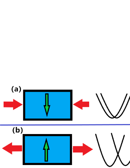
It is a natural idea to turn on and off Rashba spin-splitting through an external electric field. As shown Figure 1 (a), a 2D Janus material with a built-in electric field possesses Rashba spin-splitting. By applying an appropriate positive electric field along direction, the Rashba spin-splitting is enhanced. However, when the applied electric field is reversed (=-), the Rashba spin-splitting will disappear. In experiment, the external electric field can be as high as 0.3 ee . To accomplish our proposal practically, a 2D Janus material should meet these conditions: (1) there is a Rashba spin-splitting, and it’s better to be at the point; (2) the electronegativity difference between the bottom and top atoms is small, which will induce small built-in electric field; (3) there are heavy elements, which may produce observable Rashba spin-splitting and remedy for small built-in electric field.
The MoSSe is a representative 2D Janus material, which has been synthesized experimentallye2 ; e1 . However, the magnitude of the inherent electric field of MoSSe is 0.856 y11 , which is beyond the available experimental size of electric field (0.3 )ee . It has been proved that the Rashba spin-splitting of MoSSe still maintains by applying the external electric field of -0.5 y11-1 . Recently, the large-gap QSHIs and monolayers are predicted with -like crystal structurey11-2 , and they have sandwich structures. The Na atoms are connected with Bi atoms forming a graphene-like sheet in the ab plane, while the K/Rb atoms are above and below NaBi layer. In this work, we construct a Janus RbKNaBi material by replacing one of two K/Rb layers with Rb/K atoms in monolayer /. The artificial RbKNaBi meets the three conditions mentioned above to switch Rashba spin-splitting by reversing electric-field direction. By the first-principle calculations, our idea is illustrated in Janus monolayer RbKNaBi as a QSHI. It is found that the increasing positive external electric field can enhance Rashba energy () and Rashba constant (). However, the increasing negative external electric field firstly quenches Rashba spin-splitting, and then recover it again. In a certain electric field region, simply reversing electric-field direction can switch Rashba spin-splitting. Finally, the piezoelectric properties of RbKNaBi are studied, and the strain-induced electric field by piezoelectric effect can be used to tune Rashba spin-splitting of RbKNaBi. Our proposed manipulation of the Rashba spin-splitting can be used for future spintronic devices.
The rest of the paper is organized as follows. In the next section, we shall give our computational details and methods. In the next few sections, we shall present crystal Structure and structural Stability, electronic structures along with electric field effects and piezoelectric properties of Janus monolayer RbKNaBi. Finally, we shall give our discussion and conclusion.
II Computational detail
Within density functional theory (DFT)1 , the first-principles calculations are carried out using the projected augmented wave (PAW) method with a kinetic cutoff energy of 500 eV, as implemented in the Vienna ab initio simulation package (VASP)pv1 ; pv2 ; pv3 . The generalized gradient approximation (GGA) of Perdew, Burke and Ernzerhofpbe is adopted as the exchange-correlation potential. The total energy convergence criterion of eV and residual force of less than 0.0001 on each atom are set to obtain accurate results. A vacuum spacing of larger than 16 along the direction is included to avoid interactions between two neighboring images. The SOC is incorporated for band structure calculations.
The phonon dispersions are performed using a finite difference approach with a supercell of 551, as implemented in Phonopy codepv5 . We calculate the elastic stiffness tensor and piezoelectric stress coefficients by using strain-stress relationship (SSR) and density functional perturbation theory (DFPT) methodpv6 , respectively. The 2D elastic coefficients and piezoelectric stress coefficients have been renormalized by the the length of unit cell along direction (): = and =. A -centered 12 121 k-point meshes in the Brillouin zone (BZ) is adopted to calculate and electronic structures, and a 8121 Monkhorst-Pack k-point meshes for . The WannierTools codew1 is used to investigate topological properties of RbKNaBi, based on the tight-binding Hamiltonians constructed from maximally localized Wannier functions, as implemented in Wannier90 codew2 . The PYPROCAR code is used to obtain the constant energy contour plots of the spin texturepy .
III Crystal Structure and Structural Stability
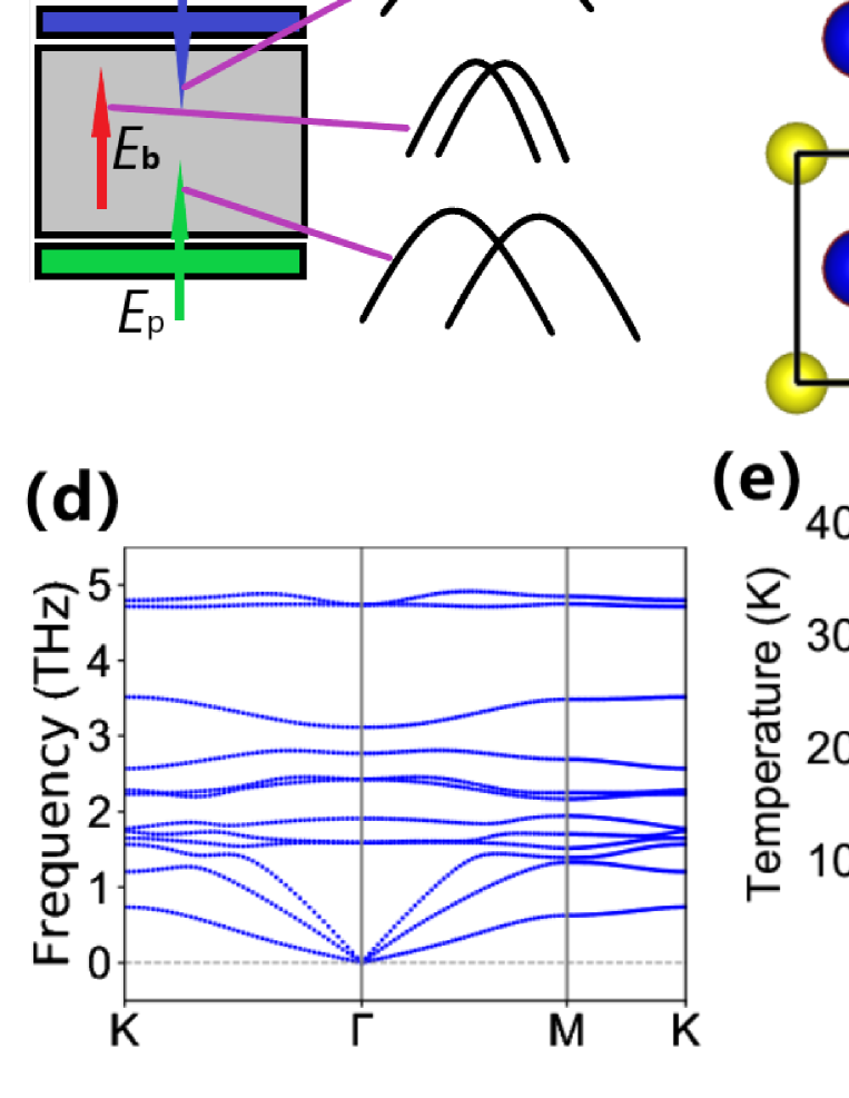
As shown in Figure 1 (b) and (c), the RbKNaBi monolayer shares the honeycomb crystal with the space group of (No.156). The Na, K and Rb atoms are all bonded to the surrounding three Bi atoms, and Na and Bi atoms form a layer, while K and Rb atoms form two more layers. The symmetry of RbKNaBi is lower than that of / with the space group of (No.187). The RbKNaBi and / all lack the spatial inversion symmetry. Besides, the RbKNaBi also lacks horizontal mirror symmetry, which will induce out-of-plane piezoelectricity and Rashba effect. The Janus monolayer RbKNaBi can be constructed by replacing one of two K/Rb layers with Rb/K atoms in monolayer /. The optimized lattice parameters of RbKNaBi is 5.587 , which is between ones of (5.548 ) and (5.629 ).
The phonon spectra, ab initio molecular dynamics (AIMD) simulations and elastic constants are calculated to confirm the stability of RbKNaBi. As shown in Figure 1 (d), no imaginary vibrational frequency can be observed, which clearly suggests that the RbKNaBi is dynamically stable. Moreover, both linear and flexural modes can be observed around the point, which shares the general features of 2D materialsr1 ; r2 . The AIMD simulation is performed by using the canonical (NVT) ensemble with a 441 supercell at 300 K for 8 ps with a time step of 1 fs. As shown in Figure 1 (e), the total energy and temperature fluctuate in the simulation time, but the average energy and temperature remain almost invariant. The final atomic configuration shows no obvious distortion of the geometric structure after 8000 steps of AIMD simulation, which can allow returning to its initiating structure by optimizing this final configuration. These results indicate its thermal stability of RbKNaBi at room temperature.
Due to symmetry, the 2D elastic tensor with using Voigt notation can be reduced into:
| (2) |
The calculated two independent elastic constants =18.40 and =5.01 , which meet the Born criteria of mechanical stability ela : and , confirming its mechanical stability. The shear modulus equals to (-)/2 (6.70 ). We calculate the direction-dependent Young’s modulus ela1 :
| (3) |
where . Calculated results show that the RbKNaBi is mechanically isotropic due to symmetry. The of RbKNaBi is 17.04 , which is between ones of ( 18.83 ) and (16.44 )y11-2 . The RbKNaBi monolayer demonstrates larger mechanical flexibility than those of other well-known 2D materials (graphene and )q5-1 ; q5-1-1 . It is found that the Poisson’s ratio is independent of direction, and can be simply expressed as:
| (4) |
The calculated is 0.272.
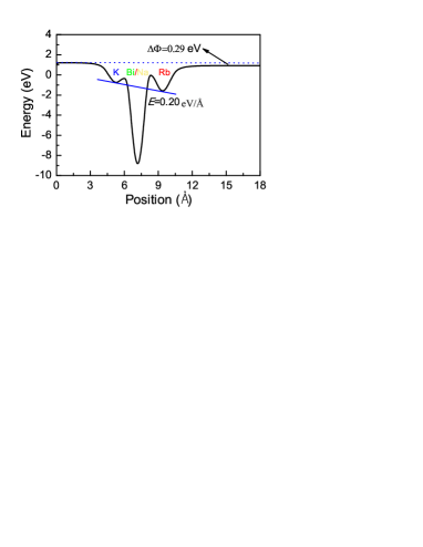
Intrinsic polar electric field is responsible for the emergence of out-of-plane piezoelectricity and Rashba effect. The difference in atomic size and electronegativity of K and Rb atoms leads to inequivalent Bi-K and Bi-Rb bond lengths (3.727 and 3.855 ), and K-Bi-K and Rb-Bi-Rb bond angles (97.12 and 92.90 ∘), giving rise to a net electric field pointing from the K layer to the Rb layer. To identify the inherent electric field further, the planar average of the electrostatic potential energy is plotted in Figure 2. The mirror asymmetry produces an electrostatic potential gradient () of about 0.29 eV, which is related to the work function change of the structure. The magnitude of the net vertical electric field is estimated to be 0.20 , which is determined by the slope of the plane-averaged electrostatic potential between K and Rb atoms’ minima. The predicted net vertical electric field is smaller than that of Janus MoSSe (0.856 )y11 , implying a weak vertical polarization. The small built-in electric field makes for switching Rashba spin-splitting by reversing electric-field direction.
| Name | ||||||||||
|---|---|---|---|---|---|---|---|---|---|---|
| 19.46 | 5.29 | 0.15 | 0.66 | 0.81 | – | – | – | 5.69 | – | |
| RbKNaBi | 18.41 | 5.02 | 0.23 | 0.51 | 0.74 | -0.071 | -0.024 | -0.095 | 5.52 | -0.41 |
| 17.08 | 4.51 | 0.293 | 0.348 | 0.641 | – | – | – | 5.10 | – |
IV electronic structures and electric field effects
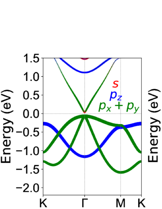
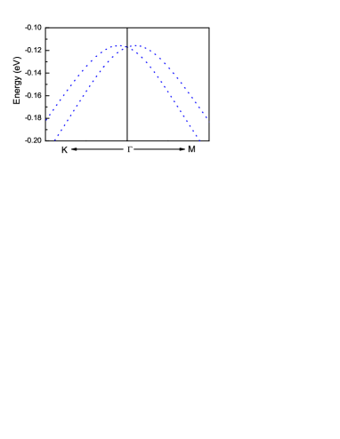
Monolayer and are predicted are large-gap QSHIsy11-2 . The nontrivial topological properties may be broken by building Janus structure from a QSHI, for example Janus and MoSSe as derivatives of QSHIs and 1-gsd4 ; gsd4-1 . Next, we investigate the electronic properties of RbKNaBi from GGA and GGA+SOC, and the Bi-, and projected band structures are plotted in Figure 3. The GGA results show that RbKNaBi has a direct band gap of 0.110 eV with valence band maximum (VBM) and conduction band minimum (CBM) at the point. However, the GGA+SOC results show an indirect band gap of 0.229 eV, and the VBM has a slight deviation from the point. The calculated gap within SOC is close to those of (0.18 eV) and (0.22 eV)y11-2 . Without considering SOC, Bi- orbitals contribute to the VBM, while the CBM is dominated by Bi- states. When including SOC, an inversion of Bi- and Bi- states can be observed in the band structures, suggesting that monolayer RbKNaBi is a QSHI. On the other hand, the SOC can lift the degenerate spins due to relativistic effects. For Janus structures, the mirror asymmetry can produce built-in electric field, leading to Rashba spin-splitting (see Figure 4). The strength of the Rashba effect can be quantized by the Rashba energy () and Rashba constant (), and the with for the Rashba momentum (see FIG.1 of electronic supplementary information (ESI)). The calculated = 1.3 meV and =0.274 .
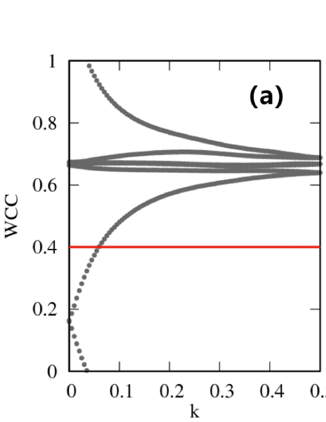
To further confirm nontrivial topological properties of RbKNaBi, we calculate the topological invariant. For a material with inversion symmetry, we can calculate topological invariant by the product of parities of all occupied states at four time-reversal-invariant-momentum points in the 2D BZ. However, for RbKNaBi with broken spatial inversion symmetry, the can be obtained by the calculation of Wannier charge center (WCC)wcc . If equals 1, a material is a topologically nontrivial, while 0 means trivial state. As plotted in Figure 5 (a), the evolution lines of WCC cross an odd number of times by an arbitrary reference line, giving rise to =1, which indicates that monolayer RbKNaBi is a QSHI. The projected edge spectra along the [100] direction is calculated, and the local density of states (LDOS) is shown in Figure 5 (b). It is clearly seen that there is a single pair of helical edge states in the bulk bandgap. Remarkably, a sizeable bulk gap (229 meV) makes for observing the room-temperature quantum spin Hall (QSH) effect, because the large gap can stabilize the helical edge states against the interference of the thermally activated carriers.
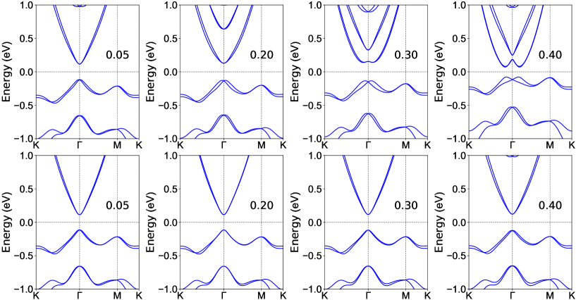
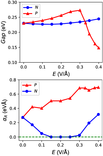
A perpendicular electric field is used to explore the manipulation of the Rashba spin splitting of RbKNaBi. There are different atomic species on its upper and lower facets for Janus RbKNaBi, implying that applying and directional electric field are not equivalent. The energy band structures as a function of electric field are calculated by using GGA+SOC. Some representative energy band structures are plotted in Figure 6, and the energy band gap vs are shown in Figure 7. In considered positive range, the gap firstly increases with increasing , and then has a sudden drop at =0.30 . However, the negative has small effects on gap. In considered both positive and negative ranges, the RbKNaBi is always a QSHI, and the calculated WCC evolutions at representative positive and negative =0.20 are plotted in FIG.2 of ESI.
Next, we mainly investigate electric field effects on Rashba spin splitting of RbKNaBi. The calculated as a function of both positive and negative are presented in FIG.3 of ESI. For positive case, the increases with increasing . However, for negative situation, the firstly decreases with increasing , and become almost zero in a certain region, and then increases. This is due to a competition between the external electric field and internal electric field. To clearly see the disappeared Rashba spin splitting, the enlarged valence bands centered at the point near the Fermi level at representative positive and negative =0.20 are plotted in FIG.4 of ESI. The calculated vs along both positive and negative directions are presented in Figure 7. The overall trend of vs is consistent with that of vs . It is clearly seen that the Rashba spin splitting of RbKNaBi is nonexistent, when is between negative 0.15 and 0.25 . In this region, the Rashba spin splitting will be opened by reversing electric field direction (from negative to positive ). This switch operation can expand the range of possible applications in future spintronic technology.
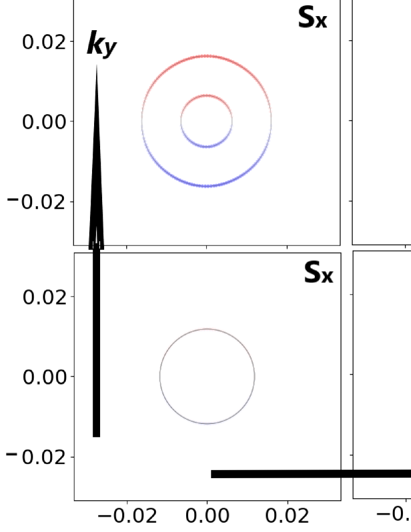
Besides , the constant energy (at an energy surface 0.16 eV below the Fermi level) spin-resolved 2D contours for the spin texture centered at the point are plotted in Figure 8 under both positive and negative 0.2 eV/. For positive case, the components have a 90∘ of rotation as compared to counterpart. The concentric spin-texture circles mean the purely 2D Rashba spin-splitting (an isotropic splitting). Only in-plane and spin components are present in the Rashba spin-splitting bands, while the out-of-plane component is non-existent, which further confirms that the spin splitting under positive 0.2 eV/ has an isotropic 2D Rashba nature. For negative situation, no Rashba spin-splitting bands can be observed. Only out-of-plane spin component is present, while in-plane and components vanish. It is clearly seen that the out-of-plane spin component has three-fold rotational symmetry.
V Piezoelectric properties
When a strain or stress is applied on a non-centrosymmetric material, the electric dipole moments can be induced and produce electricity, called piezoelectric effect. The piezoelectric response of a material can be described by third-rank piezoelectric stress tensor and strain tensor . The relaxed piezoelectric tensors ( and ) include the ionic and electronic contributions:
| (5) |
and
| (6) |
in which , and are polarization vector, strain and stress, respectively, and the superscripts and is used to denote electronic and ionic contributions. The and are also called clamped-ion piezoelectric coefficients, while and mean relax-ion cases. The is related with by elastic tensor :
| (7) |
With respect to and , for RbKNaBi, the introduction of Janus structure results in a lower degree of symmetry, and both the in-plane and out-of-plane piezoelectric effects are allowed, when a uniaxial in-plane strain is applied. By using Voigt notation, the 2D piezoelectric stress and strain tensors can be expressed asq5 ; q5-11 :
| (8) |
| (9) |
It is found that only out-of-plane piezoelectric response can exist (/=0, but /0), when applying a biaxial in-plane strain. In other words, the pure out-of-plane piezoelectric response can be realized by imposed biaxial strain. Here, the two independent and can be derived by :
| (10) |
We use the orthorhombic supercell (see Figure 1 (b)) to calculate the / of RbKNaBi. The predicted / is 0.74/-0.095 C/m with ionic part 0.51/-0.024 C/m and electronic part 0.23/-0.071 C/m. For both and , the electronic and ionic parts have superposed contributions. Based on Equation 10, the predicted / is 5.52/-0.41 pm/V. The predicted and (absolute value) are higher than or compared with those of familiar 2D materialsq5 ; q5-11 . The along direction can also be induced with a biaxial in-plane strain by piezoelectric effect, and then tune Rashba spin-splitting of RbKNaBi. When an in-plane vibration is applied to RbKNaBi, the Rashba effect will be modulated periodically. As shown in Figure 9 (a), the compressive strain induce negative electric field, which can reduce Rashba spin-splitting. However, Figure 9 (b) shows that the tensile strain induce positive electric field, which can enhance Rashba spin-splitting.
The monolayer and possess horizontal mirror symmetry, and only in-plane can exist, when a uniaxial in-plane strain is applied.For comparison, we also calculate the piezoelectric coefficients of and , and the related data are listed in Table 1. It is found that the of the three monolayers are very close, and the of RbKNaBi monolayer fall in between those of the and monolayers, as expected. The coexistence of piezoelectricity and nontrivial topological insulating phase, namely piezoelectric quantum spin Hall insulator (PQSHI), has potential advantages toward the development of high-speed and dissipationless electronic devices. Combining their nontrivial electronic structures, , and RbKNaBi all are PQSHIs.
VI Discussion and Conclusion
Some suggestions on experimental synthesis aspects of RbKNaBi are discussed. Firstly, the dynamically stable bulk compounds and are thermodynamically stable against disproportionation into the competing phasesbu . Secondly, by exfoliating these -like alkali bismide three-dimensional Dirac semimetals and , their monolayer structures are also dynamically, thermally and mechanically stabley11-2 . Finally, similar to Janus monolayer MoSSe from e1 ; e2 , the RbKNaBi can be synthesized experimentally with similar experimental techniques based on or monolayer.
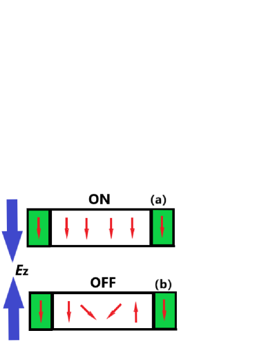
The SOC effects (Rashba spin-splitting) can be reversibly turned on and off by reversing electric-field direction, which provides a high-speed switch for the subsequent development of spin devices to control the passage of electrons (see Figure 10). For example, two ferromagnetic electrodes in the same direction are set for the component. With an appropriate negative applied electric field, the injected electrons pass through the RbKNaBi channel at a high speed and keep the spin orientation unchanged (Figure 10 (a)). When the external electric field direction is reversed, the spin of electrons in the channel will rotate under the effect of SOC, and will be blocked by the derived electrode (Figure 10 (b)). This possible spintronic device realizes the function of spintronic switch.
In summary, we have demonstrated that Rashba spin-splitting can be reversibly turned on and off by reversing electric-field direction in RbKNaBi. Calculated results show that the and are increased by the positive , while a negative suppresses the Rashba splitting to disappear, and then appears again. In a certain electric field region, simply reversing electric-field direction can achieve switching Rashba spin-splitting. Besides, it is proved that RbKNaBi is a QSHI and possesses excellent piezoelectric properties, which makes RbKNaBi become a multifunctional 2D material. Our findings can inspire more works about electric filed-tuned switch of Rashba spin-splitting.
Acknowledgements.
This work is supported by Natural Science Basis Research Plan in Shaanxi Province of China (2021JM-456). We are grateful to Shanxi Supercomputing Center of China, and the calculations were performed on TianHe-2.References
- (1) J. J. Chen, K. Wu, W. Hu and J. L. Yang, J. Phys. Chem. Lett. 12, 12256 (2021).
- (2) G. Dresselhaus, Phys. Rev. 100, 580 (1955).
- (3) Y. A. Bychkov and E. I. Rashba, JETP Lett. 39, 78 (1984).
- (4) J. Nitta, T. Akazaki, T. H. Takayanagi and T. Enoki, Phys. Rev. Lett. 78, 1335 (1997).
- (5) S. Singh and A. H. Romero, Phys. Rev. B 95, 165444 (2017).
- (6) K. Wu, J. Chen, H. Ma, L. Wan, W. Hu, and J. Yang, Nano Lett. 21, 740 (2021).
- (7) Y. Ma, Y. Dai, W. Wei, X. Li and B. Huang, Phys. Chem. Chem. Phys. 16, 17603 (2014).
- (8) H. L. Zhuang, V. R. Cooper, H. Xu, P. Ganesh, R. G. Hennig, P. Kent, Phys. Rev. B 92, 115302 (2015).
- (9) C. Liu, H. Gao, Y. Li, K. Wang, L. A. Burton and W. J. Ren, Mater. Chem. C 8, 5143 (2020).
- (10) L. Zhu, T. Zhang, G. Chen and H. Chen, Phys. Chem. Chem. Phys. 20, 30133 (2018).
- (11) D. Domaretskiy, M. Philippi, M. Gibertini, N. Ubrig, I. Gutirrez-Lezama and A. F. Morpurgo, Nat. Nanotechnol. (2022).https://doi.org/10.1038/s41565-022-01183-4
- (12) J. Zhang, S. Jia, I. Kholmanov, L. Dong, D. Er, W. Chen, H. Guo, Z. Jin, V. B. Shenoy, L. Shi and J. Lou, ACS Nano 11, 8192 (2017).
- (13) A.-Y. Lu, H. Zhu, J. Xiao, C.-P. Chuu, Y. Han, M.-H. Chiu, C.-C. Cheng, C.-W. Yang, K.-H. Wei, Y. Yang, Y. Wang, D. Sokaras, D. Nordlund, P. Yang, D. A. Muller, M.-Y. Chou, X. Zhang and L.-J. Li, Nat. Nanotechnol. 12, 744 (2017).
- (14) Y. Chen, J. Y. Liu, J. B. Yu, Y. G. Guo and Q. Sun, Phys. Chem. Chem. Phys. 21, 1207 (2019).
- (15) T. Hu, F. H. Jia, G. D. Zhao, J. Y. Wu, A. Stroppa and W. Ren, Phys. Rev. B 97, 235404 (2018).
- (16) J. W. Jiang, X. Q. Guo, Z. Ma, G. Wang, Y. G. Xu and X. W. Zhang, J. Mater. Chem. C 10, 11329 (2022).
- (17) P. Hohenberg and W. Kohn, Phys. Rev. 136, B864 (1964); W. Kohn and L. J. Sham, Phys. Rev. 140, A1133 (1965).
- (18) G. Kresse, J. Non-Cryst. Solids 193, 222 (1995).
- (19) G. Kresse and J. Furthmller, Comput. Mater. Sci. 6, 15 (1996).
- (20) G. Kresse and D. Joubert, Phys. Rev. B 59, 1758 (1999).
- (21) J. P. Perdew, K. Burke and M. Ernzerhof, Phys. Rev. Lett. 77, 3865 (1996).
- (22) A. Togo, F. Oba, and I. Tanaka, Phys. Rev. B 78, 134106 (2008).
- (23) X. Wu, D. Vanderbilt and D. R. Hamann, Phys. Rev. B 72, 035105 (2005).
- (24) Q. Wu, S. Zhang, H. F. Song, M. Troyer and A. A. Soluyanov, Comput. Phys. Commun. 224, 405 (2018).
- (25) A. A. Mostofia, J. R. Yatesb, G. Pizzif, Y.-S. Lee, I. Souzad, D. Vanderbilte and N. Marzarif, Comput. Phys. Commun. 185, 2309 (2014).
- (26) U. Herath, P. Tavadze, X. He, E. Bousquet, S. Singh, F. Munoz and A. H. Romero, Computer Physics Communications 251, 107080 (2020).
- (27) E. Mariani and F. V. Oppen, Phys. Rev. Lett. 100, 076801 (2008).
- (28) J. Carrete , W. Li, L. Lindsay, D. A. Broido, L. J. Gallego and N. Mingo, Mater. Res. Lett. 4, 204 (2016).
- (29) R. C. Andrew, R. E. Mapasha, A. M. Ukpong and N. Chetty, Phys. Rev. B 85, 125428 (2012).
- (30) E. Cadelano, P. L. Palla, S. Giordano and L. Colombo, Phys. Rev. B 82, 235414 (2010).
- (31) K. N. Duerloo, M. T. Ong and E. J. Reed, J. Phys. Chem. Lett. 3, 2871 (2012).
- (32) C. Lee, X. g Wei, J. W. Kysar and J. Hone, Science 321, 385 (2008).
- (33) S. D. Guo, Y. T. Zhu, W. Q. Mu and X. Q. Chen, J. Mater. Chem. C 9, 7465 (2021).
- (34) H. W. Xu, H. Wang, J. Zhou, Y. F. Guo, J. Kong and J. Li, npj Computational Materials 7, 31 (2021).
- (35) A. A. Soluyanov and D. Vanderbilt, Phys. Rev. B 83, 235401 (2011).
- (36) M. N. Blonsky, H. L. Zhuang, A. K. Singh and R. G. Hennig, ACS Nano, 9, 9885 (2015).
- (37) L. Dong, J. Lou and V. B. Shenoy, ACS Nano, 11, 8242 (2017).
- (38) X. Chen, W. Chen, S. Yu, S. Xu, X. Rong, P. Huang, X. Zhang and S. H. Wei, J. Mater. Chem. C 8, 1257 (2020).