Callipepla: Stream Centric Instruction Set and Mixed Precision for Accelerating Conjugate Gradient Solver
Abstract.
The continued growth in the processing power of FPGAs coupled with high bandwidth memories (HBM), makes systems like the Xilinx U280 credible platforms for linear solvers which often dominate the run time of scientific and engineering applications. In this paper, we present Callipepla, an accelerator for a preconditioned conjugate gradient linear solver (CG). FPGA acceleration of CG faces three challenges: (1) how to support an arbitrary problem and terminate acceleration processing on the fly, (2) how to coordinate long-vector data flow among processing modules, and (3) how to save off-chip memory bandwidth and maintain double (FP64) precision accuracy. To tackle the three challenges, we present (1) a stream-centric instruction set for efficient streaming processing and control, (2) vector streaming reuse (VSR) and decentralized vector flow scheduling to coordinate vector data flow among modules and further reduce off-chip memory accesses with a double memory channel design, and (3) a mixed precision scheme to save bandwidth yet still achieve effective double precision quality solutions. To the best of our knowledge, this is the first work to introduce the concept of VSR for data reusing between on-chip modules to reduce unnecessary off-chip accesses for FPGA accelerators. We prototype the accelerator on a Xilinx U280 HBM FPGA. Our evaluation shows that compared to the Xilinx HPC product, the XcgSolver, Callipepla achieves a speedup of , higher throughput, and better energy efficiency. Compared to an NVIDIA A100 GPU which has the memory bandwidth of Callipepla, we still achieve 77% of its throughput with higher energy efficiency. The code is available at https://github.com/UCLA-VAST/Callipepla.
1. Introduction
The need to solve large systems of linear equations is common in scientific and engineering fields including mathematics, physics, chemistry, and other natural sciences subjects (Ferziger and Perić, 2002; Griewank and Walther, 2008; Antoulas, 2005), and often dominates their runtime. As these linear systems are often sparse, it is not practical to invert them, and the requirements for storage and time grow superlinearly if one tries to factor them. Therefore, for well conditioned problems, practitioners are drawn to iterative algorithms whose storage requirements are minimal, yet still converge to a useful solution in a reasonable period of time.
The Conjugate Gradients method (Hestenes and Stiefel, 1952) is a well known iterative solver. Coupled with even the simplest Jacobi preconditioner (JPCG) (Saad, 2003), it is very effective for solving linear systems that are symmetric and positive definite. The acceleration of (preconditioned) conjugate gradient on general-purpose platforms CPUs and GPUs suffer from low computational efficiency (Nakano, 1997; Helfenstein and Koko, 2012). The computational efficiency is even worse for distributed and clustered computers (Dongarra et al., 2015).
The recent High Bandwidth Memory (HBM) equipped FPGAs (Xilinx, 2022a) enable us to customize accelerator architecture and optimize data flows with high memory bandwidth for the conjugate gradient solver. In this work, we present Callipepla, an accelerator prototyped on Xilinx U280 HBM FPGA for Jacobi preconditioned conjugate gradient linear solver. We resolve three challenges in FPGA CG acceleration with our innovative solutions.
Challenge 1: The support of an arbitrary problem and accelerator termination on the fly. The FPGA synthesis/place/route flow takes hours even days to complete, which prevents the frequent invocation of conjugate gradient solvers on different problems in data centers. Thus, we need to build an accelerator to support an arbitrary problem. However, the JPCG has six dimensions of freedom as illustrated in Algorithm 1, which makes it challenging for the JPCG accelerator to support an arbitrary problem. Furthermore, it is difficult to terminate the accelerator on the fly for a preset threshold (Line 6 of Algorithm 1), because we do not know when to terminate until we run the algorithm/accelerator. To resolve this challenge, we design a stream centric instruction set to control the processing modules and data flows in the accelerators. We encode vector and matrix size and data flow directions in the instruction. A global controller is responsible to issue instructions. Therefore, we are able so support an arbitrary problem for JPCG and terminate the accelerator.
Challenge 2: The coordination of long-vector data flow among processing modules. JPCG involves the processing of multiple long vectors whose size is larger than on-chip memory. The latency cost is high if we always write a produced vector to off-chip memory and read a vector from off-chip memory when a module consumes the vector. There are opportunities to save off-chip memory read and write by reusing vectors among processing modules. For this challenge, we introduce the concept of vector streaming reuse and analyze the dependencies in JPCG to decide when and which vectors we may reused by processing modules via on-chip streaming and store/load the other vectors that can not be reused to/from off-chip memory. Based on the vector reusing/loading/storing analysis, we form a decentralized vector scheduling to dissolve the global control to vector control and computation modules to coordinate vector flows among modules.
Challenge 3: Saving off-chip memory bandwidth and maintaining double (FP64) precision convergence. The sparse matrix with FP64 precision dominates memory footprint and thus memory bandwidth in the sparse matrix vector multiply (SpMV) of JPCG. Lower precision (less bits per data element) provides higher parallelism. However, lower precision leads to larger iteration count for convergence or even failure to converge. To resolve this issue, we present a mixed FP32/FP64 precision for SpMV in JPCG to save memory bandwidth and achieve effective convergence as default FP64 precision.
Our evaluation Xilinx U280 HBM FPGAs shows that compared to the Xilinx HPC product XcgSolver, Callipepla achieves a speedup of , higher throughput, and better energy efficiency. Compared to an NVIDIA A100 GPU which has the memory bandwidth of Callipepla, we still achieve 77% of its throughput with higher energy efficiency.
2. CG Solver Acceleration Challenges & Callipepla Solutions
2.1. Conjugate Gradient Solver
For non-trivial problems, it is not practical nor hardware efficient to directly inverse the matrix to solve the linear system because can be very large in real-world applications. The conjugate gradient (Hestenes and Stiefel, 1952) iteratively refines errors and reaches the solution. The Jacobi preconditioner (Saad, 2003) approximates the matrix with its diagonal, which is trivial to invert. Using even this simple Jacobi preconditioner helps reduce the iteration number and accelerate the conjugate gradient method.
Algorithm 1 illustrates the Jacobi preconditioned conjugate gradient algorithm (JPCG) for solving the linear system . JPCG takes as input the matrix , the Jacobi preconditioner , i.e., the diagonal of , a reference vector , an initial solution vector , convergence threshold , and a maximum iteration count . In the algorithm, represents the error of current solution vector , the cooperation of vector , and vector helps the solution vector refine to the correct values at each iteration, and vector is the product of matrix and vector . Line 1 to 3 compute the initial values of the vectors , , and given the initial solution vector . Lines 4, 5 initialize two scalars, rz and rr. In the main loop body, the JPCG updates the vectors and scalars. Note that for the computation of , because is a diagonal matrix, the invert and multiply operation becomes an element-wise divide. In summary, the JPCG involves the coordination of multiple kernels. The sparse matrix vector multiplication SpMV, dot product, and generalized vector addition axpy are the core computations. Note, any practical implementation of the JPCG, whether on a GPU or and FPGA, will frequently invoke memory load operations to fetch the matrix and the vectors, as well as stores on the vectors. This is because the size of the linear system dwarfs the on-chip memory capacity.
We accelerate the JPCG in this work because:
The JPCG is an important solver used in the industry. For example, the JPCG is a solver in Ansys LS-DYNA (Technology, 2022), a finite element program for engineering simulation. In Xilinx Vitis HPC Libraries (Xilinx, 2022b), the JPCG is the only linear system solver.
The JPCG is hardware efficient. There are more powerful preconditioners one could consider, which generally reduce the number of iterations required to solver the linear system. For example, incomplete Cholesky factorization (ICCG) (Kershaw, 1978) employs the lower triangular matrix from an incomplete Cholesky factorization as the preconditioner matrix . But solving incurs massive dependency issues, thus, difficult to process in parallel in hardware. We will address that in future work.
2.2. Prior CG Acceleration & Related Works
CG acceleration. (Maslennikow et al., 2005) implemented the basic CG on FPGAs while the problem dimension supported is less than 1,024, thus, not practical for real-world applications. (Lopes and Constantinides, 2008) implemented a floating-point basic CG for dense matrices. The supported matrix dimension is less than 100, and it needed to generate a new hardware accelerator for every new problem instance. (Roldao-Lopes et al., 2009) explored reducing FP mantissa bits to reduce FP computation latency and resource. (Rampalli et al., 2018) implemented CG for Laplacian systems. However, (Roldao-Lopes et al., 2009; Rampalli et al., 2018) stored vectors all on chip without off-chip memory optimization and was limited to small size problems. Even the minimum throughput achieved by Callipepla is 1.35 higher than the maximum throughput achieved by (Rampalli et al., 2018). Besides, the reduced bit method of (Roldao-Lopes et al., 2009) led to considerable iteration gaps compared with default FP64, but our mixed-precision scheme makes the gap negligible. The GMRES leverages low precision in error correction computation and the inner loop (Higham and Mary, 2022) to reduce processing time. It is unexplored how to co-optimize mixed precision with memory accessing on the modern HBM FPGAs. All the prior works (Maslennikow et al., 2005; Lopes and Constantinides, 2008; Roldao-Lopes et al., 2009; Rampalli et al., 2018) did not optimize off-chip memory accesses, did not leverage preconditioners to accelerate the convergence, were not able to terminate accelerator on the fly, and were not able to perform large scale CG (where the matrix dimension can be a few hundred thousands to several millions). XcgSolver (Xilinx, 2022b, c) by Xilinx is a state-of-the-art FPGA CG solver which can run real-world large-scale CG. So we use XcgSolver as the baseline.
Other related works. GraphR (Song et al., 2018) and GraphLily (Hu et al., 2021) are accelerators based on non-traditional (other than DDR) memories for graph processing. Sextans (Song et al., 2022b) and Serpens (Song et al., 2022a) are SpMM/SpMV accelerators on HBM memories, while Fowers et al. (Fowers et al., 2014) designed an SpMV accelerator on DDR memory. Song et al. (Song et al., 2020) explored mixed precision for conjugate gradient solvers in ReRAM. TAPA (Chi et al., 2021) provides a framework for task-parallel FPGA programing, and AutoBridge (Guo et al., 2021) optimized the floor planning for high level synthesis and thus boosted the frequency of generated accelerators (Guo et al., 2022). Cheng et al. (Cheng et al., 2020, 2021) explored the combination of static and dynamic scheduling in high-level synthesis (HLS). Coarse grain reconfigurable architecture (CGRA) accelerators (Nowatzki et al., 2018; Weng et al., 2020a, 2022; Liu et al., 2022; Weng et al., 2020b; Nowatzki et al., 2017) utilize instructions to schedule computation and memory accesses.
2.3. Acceleration Challenges & Our Solutions
2.3.1. How to support an arbitrary problem and terminate acceleration processing on the fly?
Many previous FPGA accelerators support a fixed-size problem such as deep learning accelerators (Wang et al., 2021; Cong and Wang, 2018; Zhang et al., 2015), stencil computation (Chi et al., 2018; Chi and Cong, 2020), graph convolutional network acceleration (Zeng and Prasanna, 2020), and other applications (Guo et al., 2019). FPGA accelerators that support fixed-size problems need to re-perform synthesis/place/route flow for a new problem. The synthesis/place/route flow takes hours to days to finish, which is not suitable for the frequent invocation for different problems in data centers. Thus, the accelerator needs to support an arbitrary problem once deployed. However, the JPCG has six dimensions of freedom as Algorithm 1 illustrates, which makes it challenging to support an arbitrary size problem.
Another unique challenge is designing an accelerator that is able to terminate on the fly. Because the JPCG will terminate the main loop once the residual is less than a preset threshold (Line 6 of Algorithm 1), which we do not know until we run the algorithm/accelerator. In contrast, in deep learning acceleration, we know the iteration numbers of all loops before the execution.
Callipepla Solution: Stream Centric Instruction Set. We design a stream centric instruction set to control the processing modules and data flows in the accelerators. We encode vector and matrix size and data flow directions in the instruction. A global controller is responsible to issue instructions. Therefore, we are able to support an arbitrary problem for the JPCG and terminate the accelerator. There are three principles for designing our stream centric instruction set:
(1) Stream centric. Every instruction is to process some streams. The JPCG is dealing with vectors and matrices and we transfer those in streams. This principle naturally enables task parallelism.
(2) Data streamed processing. We introduce a processing model that will either procure or consume streams in the accelerator. We use an instruction to control the behavior of a processing module.
(3) Decoupled memory and computing. We separate the memory load/store from computation. In this way, we can benefit from prefetching and overlapped computing and memory accessing.
2.3.2. How to coordinate long-vector data flow among processing modules?
The vector length in a real-world JPCG problem could be a few thousand to more than one million as shown in Table 3. Because we process floating-point values, one vector size will be up to tens of megabytes which exceeds the on-chip memory size. One straightforward way is that we always store an output vector from a processing module to the off-chip memory and load an input vector from the off-chip memory to a module. However, there are reuse opportunities to save some off-chip memory load and store in JPCG. For example, the output vector by Line 7 will be consumed by Line 8 and Line 10. But it is non-trivial to reuse for Line 10 during streaming because there is a dependence (i.e., ) of Line 10 on Line 8, and Line 8 will not produce until it consumes the whole vector . As a result, we need to store the whole on chip for reusing, which is not practical. Therefore, we have a dilemma: (1) vector exceeds the on-chip memory size so we need to store it in the off-chip memory, but (2) we need to reuse to reduce off-chip memory accesses, however, (3) the dependence issue requires us to store the whole vector on chip or there will be no reuse. Therefore, it is a challenge to coordinate vector flows among processing modules for reusing while resolving the dependence issue at the same time.
Callipepla Solution: Decentralized Vector Scheduling. In Section 5 we will introduce the concept of vector streaming reuse and analyze the dependency in the JPCG and partition the main loop in three phases so that we will reuse vectors within the same phase via on-chip streaming while store/load vectors to/from memory across phases. Based on the vector reusing/loading/storing, we will form a decentralized vector scheduling to dissolve the global control to vector control and computation modules to coordinate vector flows among modules.
2.3.3. How to save off-chip memory bandwidth and maintain double (FP64) precision?
To represent a double-precision (FP64) non-zero, we need 32 bits for the row index, 32 bits for the column index, and 64 bits for the FP64 value. So we need 128 bits to represent an FP64 non-zero. Similarly, we need 96(=32+32+32) bits to represent an FP32 non-zero. The memory port has a limited bit width. For example, the AXI bus width is up to 512 bits (Cong et al., 2018; Choi et al., 2021). Therefore, lower precision (less bits per data element) provides higher parallelism. However, the default JPCG requires the FP64 precision for convergence. There are many vectors and one sparse matrix in the JPCG. How can we configure the precision (FP32 or FP64) for the vectors and matrix in the JPCG to save memory bandwidth but also converge as effective as the default FP64 precision?
| Default FP64 | FP64 | FP64 | FP64 |
| Mixed-V1 | FP32 | FP32 | FP32 |
| Mixed-V2 | FP32 | FP32 | FP64 |
| Mixed-V3 | FP32 | FP64 | FP64 |
Callipepla Solution: Mixed-precision SpMV. Because the JPCG refines vectors in the main loop, we must maintain all vectors in FP64 at the end of each iteration. The SpMV takes as input one vector and one sparse matrix and output a vector . Among the two vectors and one matrix, the sparse matrix dominates the memory footprint. Thus, we consider using FP32 for the sparse matrix. For the SpMV input/output vectors, we have two precision options – FP32 or FP64. Thus, we have three mix-precision schemes, illustated in Table 1. Noted the mixed precision only applies to the SpMV, and we always maintain the the vectors in the main loop in FP64. We will discuss the mixed precision in Callipepla and the hardware design for supporting mixed-precision SpMV in Section 6.
3. Callipepla Architecture
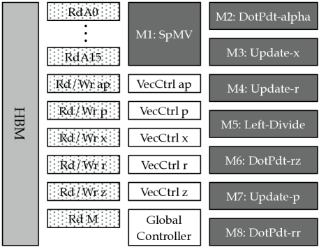
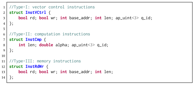
Figure 1 shows the top architecture of Callipepla accelerator which is a modular architecture. There are four categories of modules – (1) computation units, (2) read/write modules, (3) vector control modules, and (4) a global controller. All modules are connected via FIFOs.
Computation modules perform the vector/matrix computations. We have eight computation modules – (1) M1: SpMV, performing the computation of Line 7 in Algorithm 1, (2) M2: dot product alpha, performing the computation of Line 8, (3) M3: update x, performing the computation of Line 9, (4) M4: update r, performing the computation of Line 10, (5) M5: left divide, performing the computation of Line 11, (6) M6: dot product rz, performing the computation of Line 12, (7) M7: update p, performing the computation of Line 13, and (8) M8: dot product rr performing the computation of Line 15. For Line 1 to Line 5, we reuse the eight computation modules to perform the computation. We leverage the open-sourced Serpens (Song et al., 2022a) accelerator for SpMV computation and design the modules M2 to M8 for Callipepla.
Memory read/write modules move data from off-chip memory to on-chip modules or vice versa. We use the high bandwidth memory on Xilinx U280 FPGA as our off-chip memory. We have sixteen read A modules (RdA0 to RdA15) to read non-zeros to the SpMV module M1 and a Rd M to read the Jacobi matrix. There are five Rd/Wr (read-and-write) modules for vectors , , , , and , because the five vectors need both read and write operations. We connect each read/write module to one HBM channel.
Vector control modules VecCtrl ap, p, x, r, and z coordinate vector flows between one corresponding read/write modules to multiple computation units. For example, according to Algorithm 1, M1 (SpMV) produces vector and M2 (dot product alpha) and M4 (update r) consume . So the module VecCtrl ap coordinates vector flows among Rd/Wr ap and three computation modules M1, M2, and M4.
The global controller issues instructions to computation modules and vector control modules. The global controller also performs some scalar computation such as Line 14 of Algorithm 1 and compares to decide whether to terminate or not.
4. Stream Centric Instruction Set
4.1. Three Instruction Types
We define the instruction types as illustrated in Figure 2 for Callipepla. They are (1) Type-I: vector control instructions, (2) Type-II: computation instructions, (3) Type-III: memory instructions.
4.1.1. Type-I: vector control instructions
We use vector control instructions to tell a vector control module where and how to deliver a vector. Type-I instructions have five components – (1) int rd and (2) int wr encode whether to read or write or simultaneously read and write a vector, (3) int base_addr encodes the base address of a vector in the memory, (4) int len encodes the vector length, and (5) ap_uint<3> q_id encodes the index of a destination module where to send the vector.
4.1.2. Type-II: computation instructions
We use computation instructions to trigger the execution of a computation module and where to send the output vector. Type-II instructions have three components – (1) int len encodes the vector length, (2) double alpha a double-precision constant scalar involved in the computation, and (3) ap_uint<3> q_id encodes the index of a destination module where to send the vector. Note that the computation instructions do not have operation code because a computation module in the accelerator only has one function.
4.1.3. Type-III: memory instructions
We use memory instructions to read a vector from off-chip memory to a vector control module or write a vector from a vector control module to off-chip memory. Type-III instructions have three components – (1) int rd and (2) int wr encodes whether to read or write or simultaneously read and write a vector, (3) int base_addr encodes the base address of a vector in the memory, and (4) int len encodes the vector length.
4.2. Processing Model
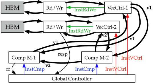
Figure 3 displays an example where we process two vectors with two computation modules. A global controller issues vector control instructions to the two vector control modules VecCtrl-1 and VecCtrl-2. v1 and v2 are two vectors, rr is a scalar, and resp is a memory response.
Vector flow. Instructions control vector flow among modules in a streaming fashion. For example, if we are reading vector v1 with a length 100 from memory to Comp M-2, the controller will issue an instruction InstVCtrl{rd=1, wr=0, base_addr=0, len=100, q_id=1} to VecCtrl-1. Here, q_id=1 indicates the destination module is M-2 rather than M-1. Then VecCtrl-1 will issue a memory instruction InstRdWr{rd=1, wr=0, base_addr=0, len=100} to the memory module. Next, vector v1 flows from the memory to Comp M-2. Another example is that the controller issues a computation instruction InstCmp{len=100, alpha=2.0, q_id=1} to Comp M-2. We assume M-2 performs . Then M-2 will consume the input v1 and v2 vectors and deliver the result vector v2(=v2 + 2.0*v1) to M-1.
Scalar and memory response. We update all scalars in the global controller. For instance, Comp M-1 delivers a scalar rr to the controller and the controller will decide whether to terminate the accelerator or not. At the memory modules, we always send out a response to the controller if we are processing a memory write operation. The response message will help the controller to maintain memory consistency when multiple modules read and write the same vectors.
Overlapped execution and prefetching. The models involved are working in parallel, i.e., task parallelism, because we never cache a whole vector on chip. One element in an input stream will be consumed by a module and sent to an output vector flow at each cycle. So the modules in Callipepla accelerators work with an II=1 pipeline111For the dot product modules, we have two phases. Phase I multiplies input and accumulates in a cyclic delay buffer with an II=1 pipeline. Phase II accumulates contents in the delay buffer with a larger II=5 pipeline because of the read after write dependency and the FP ADD latency. The Phase II cycle count is fixed, i.e., where is the delay buffer size, for any arbitrary length vector. So the Phase II cycle count is negligible compared to the Phase I cycle count.. We always prefetch vectors in the processing. We enable prefetching by issuing multiple instructions. For example, if Comp M-1 needs input vector v1 from memory and input vector v2 from Comp M-2, along with the computation instruction to M-2, we also issue the vector control instruction to the vector control module to read v1 to M-1 for prefetching.
Processing rate matching. Prior work (Cong et al., 2014) processing rate matching of modules in streaming applications. In this work, because we do not cache any vector on chip and we overlap the execution, we match the vector input and output streaming rate. Therefore, the bottleneck becomes the connections between a memory module and a memory channel. Although there are modules that use multiple channels, we can simplify the connection as one-module-one-channel because we can view a multi-channel module as multiple one-channel modules and they are connected via on-chip connections. Thus, we can derive the accelerator frequency that matches the memory bandwidth as
| (1) |
where is per channel memory bandwidth and is the maximum memory datawidth. For a Xilinx U280 HBM FPGA (Xilinx, 2022a) which has 32 HBM channels and 460 GB/s memory bandwidth and supports a 512-bit (64-byte) memory width (Cong et al., 2018; Choi et al., 2021), the matching frequency is MHz.
4.3. The Global Controller Code
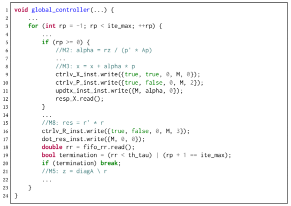
Figure 4 shows the instruction code in the global controller. We only show the main loop control code and the intrusions for vector control and computation for module M3 and M8. The code in Figure 4 is quite similar to Algorithm 1 because Callipepla’s instructions make it easy for users to control the accelerators. In the controller code, we have two optimizations – (1) We merge Line 1 to 5 of Algorithm 1 into the main for loop to reuse the modules. The if clause (Line 5 to 13) in Figure 4 skips some modules in iteration (rp=-1) so that we can perform the computation of Line 1 to 5 of Algorithm 1 using the main for loop. (2) We move the last module M8 which is the computation of residual before M5 to skip the computations of M5 to M7 once the solver converges.
5. Vector Streaming Reuse & Decentralized Vector Scheduling
5.1. Vector Streaming Reuse
The accelerator has to store long vectors to off-chip memory because of limited on-chip memory size. However, there are reusing opportunities so that we can avoid unnecessary load/store. Vector streaming reuse (VSR) means vectors are reused in a streaming fashion by processing modules via on-chip streams/FIFOs.
What is VSR? A processing module (PM) consumes an element of a vector from an input stream/FIFO and produce an element (for a processed vector) or duplicate an element (for the input vector) to an output stream/FIFO to another PM. The PMs consume/produce vector elements in pipeline and there may be multiple input/output streams/FIFOs connected to one PM.
When can VSR? (1) Multiple PMs consume the same input vector(s), (2) a PM consumes vector(s) that are produced by some other PMs, and (3) the difference of accessing indices of two input vectors is within the on-chip (or stream/FIFO) memory budget.
When can not VSR? (1) The computation of a scalar requires a whole vector and PMs has dependency on the scalar can not reuse the vector and (2) the difference of accessing indices of two input vectors is out of the on-chip (or stream/FIFO) memory budget.
5.2. Three Computation Phases
We analyze the scalar dependency and then divide the eight computation modules into three phases as shown in Figure 5. The scalar dependency is the critical issue that prevents us from reusing vectors across computation modules. For example, we can not reuse the input vector of M2 to M4 (which also takes as input) because M4 depends on alpha and alpha depends on the whole vector . So we move M4 to Phase-2. Because M5/6/8 depends on vector from M4 so we direct M5/6/8 to Phase-2. Similarly, we organize the computations in Phase-3 according to the dependency on scalar rz.
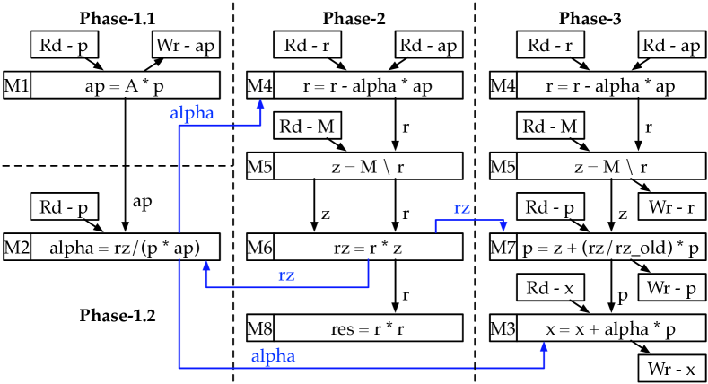
5.3. Recomputing to Save Off-Chip Memory
Among all vectors, vector is a special one because is an intermediate vector in the main loop and it is not reused between two iterations. Thus, we reduce the off-chip memory allocation for by recomputing in Phase-3. In this way, we save memory channels. Shown in Figure 5, at Phase-2 after computation module M5 produces , we do not write to memory. At Phase-3, because M7 requires as input, so we reperform both M5 and M4. M4 is the dependency of M5 to produce vector to M7.
5.4. VSR and Memory Accessing
After forming the three computation phases, we determine the VSR and the memory accessing for vectors that we have to do. Phase 1: In Phase-1.1 we perform M1 and in Phase-1.2 we perform M2. We reuse the produced by M1 to M7 to avoid reading the from off-chip memory. We cannot reuse vector from M1 for M2 because M1 outputs only after consuming the whole vector . We write vector to memory. Phase 2: We reuse vector by all the four modules M4/5/6/8. M4 consumes one entry from the input stream of vector from memory and immediately M4 sends the entry to the next module M5. M5 and M6 perform the same consume-and-send on vector so that we only need to read vector from memory once. In this phase, we also have to read vector and vector from memory once. Phase 3: Similar to Phase 2, M4 and M5 reuse vector and M7 and M3 reuse vector . We have to read vector , , , and from memory and write vector , , and to memory.
5.5. Decentralized Vector Scheduling
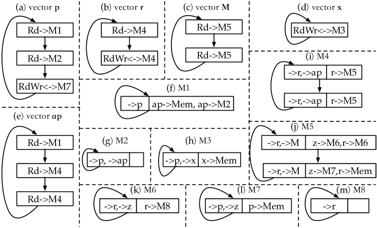
The VSR makes the control complicated because we must handle both on-chip and off-chip vector flows among all computation and vector control modules. We present decentralized vector scheduling to relieve the pressure faced by a centralized controller. Another benefit is that decentralized vector scheduling is better for the controller routing because there are 23 FIFOs for a centralized controller. We dencentralize all vector scheduling into each individual vector control module (vector , , , , and ) and into the computation modules (M1 to M8) show in Figure 6. We use a finite state machine (FSM) to control the vector flow at each module. Note that decentralized vector scheduling maintains all dependencies.
Vector scheduling in vector control modules. We use the FSM for in Figure 6 (a) to illustrate vector scheduling. According to Figure 5, there are three memory operations for : (1) Rd to M1 at Phase-1.1, (2) Rd to M2 at Phase-1.2, and (3) Rd and Wr to/from M7 at Phase-3. Thus, we have the FSM in Figure 6 (a) for scheduling.
Vector scheduling in computation modules. We use Figure 6 (j) the FSM for M5 to illustrate the scheduling. According to Figure 5, at Phase-2, M5 takes as inputs the flows of the vectors and , and outputs and to M6, resulting in the first scheduling state. At Phase-2, M5 uses the flows of vector and as inputs, but outputs to M7 and to memory, completing the second scheduling state.
Without the decentralized vector scheduling, the accelerator accesses vectors 19 times (14 reads and 5 writes). With the decentralized vector scheduling, the accelerator accesses vectors 14 times (10 reads and 4 writes).
5.6. Avoiding Deadlock
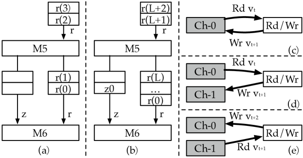
A deadlock may occur when we reuse more than one vector to a destination module. In Figure 7 (a), the default FIFO depth is 2 and the M5 (left divide) pipeline depth is . Thus, when the fast side FIFO is full but the slow FIFO is still empty, a deadlock occurs because M5 cannot write to FIFO and M6 cannot consume FIFO entries (because FIFO is empty). To resolve the deadlock, we increase the fast FIFO depth to as shown in Figure 7 (b). As a result, during cycle 0 to M5 can write FIFO despite FIFO is empty, but after cycle , M5 can write both FIFO and and M6 can read both FIFOs.
5.7. Double Channel Design
By default a memory module reads and writes to the same memory channel as shown in Figure 7 (c), which doubles the memory latency when we perform both read and write on a vector. Inspired by the widely used on-chip double buffer design in FPGA accelerators (Zhang et al., 2015; Wang et al., 2021; Sohrabizadeh et al., 2020; Zhao et al., 2017), we present a double off-chip channel design. In Figure 7 (d) and (e), we connect two channels to a memory module and at the iteration we read vector from channel 0 and write the updated to channel 1. At the iteration we read from channel 1 and write the updated to channel 0. Therefore, we reduce the memory latency by half and maintain the inter-loop vector dependency.
6. Mixed-Precision SpMV
Table 1 presents three mixed precision schemes and the default FP64 precision. Overall, a scheme with more data in FP64 is less hardware efficient because it requires larger memory capacity and higher memory bandwidth but the accuracy is higher. Mixed-V1 uses FP32 for all values in the matrix and vectors. Although Mixed-V1 is the most memory saving scheme, it is also the most inaccurate scheme. Because the JPCG is sensitive to vector precision, Mixed-V2 utilizes FP64 for the SpMV output vector. Mixed-V3 utilizes FP64 for both SpMV input and output vectors.Among the three mixed-precision schemes, Mixed-V3 does not sacrifice vector precision and at the same time saves memory for the sparse matrix. Note that in SpMV the sparse matrix dominates the memory footprint. Therefore, we use Mixed-V3 for the Callipepla accelerator for both memory efficiency and computation accuracy.
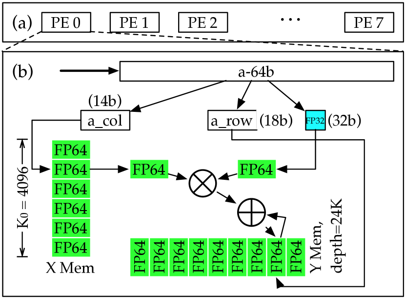
Figure 8 illustrates the mixed-precision SpMV module architecture in Callipepla. We leverage the Serpens (Song et al., 2022a) architecture. Each SpMV module is connected to one memory channel and has eight parallel processing engines. The input to a processing engine is a 64-bit element which contains a 14-bit column index, an 18-bit row index, and an FP32 value. For the mixed-precision SpMV, we (1) store the input FP64 vector in an on-chip X memory implemented by BRAMs, and (2) buffer the output FP64 vector in an on-chip Y memory implemented by URAMs. The depths of the X and Y memories are 4K and 24K respectively. In the processing pipeline, we (1) cast the FP32 sparse value into a FP64 value, (2) use the column index to fetch the corresponding input element from the X memory, (3) then multiply the two FP64 scalars, and (4) accumulate the result to the Y memory entry indexed by row.
7. Evaluation
| Process | Frequency | Memory | Bandwidth | Power | |
|---|---|---|---|---|---|
| XcgSolver | 16 nm | 250 MHz | 8 GB | 331 GB/s | 49 W |
| SerpensCG | 16 nm | 238 MHz | 8 GB | 345 GB/s | 43 W |
| Callipepla | 16 nm | 221 MHz | 8 GB | 374 GB/s | 56 W |
| NVIDIA A100 | 7 nm | 1.41 GHz | 40 GB | 1.56 TB/s | 243 W |
| ID | Matrix | #Row | NNZ | ID | Matrix | #Row | NNZ | ID | Matrix | #Row | NNZ |
|---|---|---|---|---|---|---|---|---|---|---|---|
| M1 | ex9 | 3,363 | 99,471 | M2 | bcsstk15 | 3,948 | 117,816 | M3 | bodyy4 | 17,546 | 121,550 |
| M4 | ted_B | 10,605 | 144,579 | M5 | ted_B_unscaled | 10,605 | 144,579 | M6 | bcsstk24 | 3,562 | 159,910 |
| M7 | nasa2910 | 2,910 | 174,296 | M8 | s3rmt3m3 | 5,357 | 207,123 | M9 | bcsstk28 | 4,410 | 219,024 |
| M10 | s2rmq4m1 | 5,489 | 263,351 | M11 | cbuckle | 13,681 | 676,515 | M12 | olafu | 16,146 | 1,015,156 |
| M13 | gyro_k | 17,361 | 1,021,159 | M14 | bcsstk36 | 23,052 | 1,143,140 | M15 | msc10848 | 10,848 | 1,229,776 |
| M16 | raefsky4 | 19,779 | 1,316,789 | M17 | nd3k | 9,000 | 3,279,690 | M18 | nd6k | 18,000 | 6,897,316 |
| M19 | 2cubes_sphere | 101,492 | 1,647,264 | M20 | cfd2 | 123,440 | 3,085,406 | M21 | Dubcova3 | 146,689 | 3,636,643 |
| M22 | ship_003 | 121,728 | 3,777,036 | M23 | offshore | 259,789 | 4,242,673 | M24 | shipsec5 | 179,860 | 4,598,604 |
| M25 | ecology2 | 999,999 | 4,995,991 | M26 | tmt_sym | 726,713 | 5,080,961 | M27 | boneS01 | 127,224 | 5,516,602 |
| M28 | hood | 220,542 | 9,895,422 | M29 | bmwcra_1 | 148,770 | 10,641,602 | M30 | af_shell3 | 504,855 | 17,562,051 |
| M31 | Fault_639 | 638,802 | 27,245,944 | M32 | Emilia_923 | 923,136 | 40,373,538 | M33 | Geo_1438 | 1,437,960 | 60,236,322 |
| M34 | Serena | 1,391,349 | 64,131,971 | M35 | audikw_1 | 943,695 | 77,651,847 | M36 | Flan_1565 | 1,564,794 | 114,165,372 |
| M1 | M2 | M3 | M4 | M5 | M6 | M7 | M8 | M9 | ||
| XcgSolver(s) | 8.973E-1 | 4.151E-2 | 3.634E-2 | 3.825E-3 | 3.792E-3 | 5.219E-1 | 9.691E-2 | 1.268 | 3.577E-1 | |
| SerpensCG(s) | 8.010E-1 | 2.787E-2 | 2.357E-2 | 2.656E-3 | 2.656E-3 | 4.217E-1 | 7.386E-2 | 1.245 | 2.719E-1 | |
| Speedup | 1.120 | 1.490 | 1.542 | 1.440 | 1.428 | 1.238 | 1.312 | 1.018 | 1.315 | |
| Callipepla(s) | 2.602E-1 | 9.200E-3 | 6.579E-3 | 9.261E-4 | 9.376E-4 | 1.408E-1 | 3.020E-2 | 4.213E-1 | 1.021E-1 | |
| Speedup | 3.449 | 4.512 | 5.524 | 4.131 | 4.045 | 3.705 | 3.209 | 3.009 | 3.502 | |
| A100(s) | 1.752 | 5.430E-2 | 1.510E-2 | 3.681E-3 | 2.455E-3 | 8.292E-1 | 2.076E-1 | 1.348 | 5.183E-1 | |
| Speedup | 5.120E-1 | 7.645E-1 | 2.406 | 1.039 | 1.545 | 6.294E-1 | 4.667E-1 | 9.407E-1 | 6.901E-1 | |
| M10 | M11 | M12 | M13 | M14 | M15 | M16 | M17 | M18 | GeoMean | |
| XcgSolver(s) | 1.613E-1 | 2.309E-1 | 3.336 | 3.333 | 4.540 | 1.246 | 4.883 | 3.813 | 1.018E+1 | |
| SerpensCG(s) | 1.162E-1 | 2.019E-1 | 4.103 | 2.983 | 5.333 | 1.050 | 5.076 | 3.238 | 7.970 | |
| Speedup | 1.389 | 1.143 | 8.130E-1 | 1.117 | 8.513E-1 | 1.187 | 9.621E-1 | 1.178 | 1.277 | 1.194 |
| Callipepla(s) | 4.103E-2 | 7.104E-2 | 1.488 | 1.243 | 1.872 | 4.577E-1 | 1.853 | 1.580 | 3.785 | |
| Speedup | 3.932 | 3.249 | 2.242 | 2.681 | 2.425 | 2.723 | 2.636 | 2.413 | 2.689 | 3.241 |
| A100(s) | 1.639E-1 | 1.227E-1 | 2.074 | 1.298 | 1.903 | 6.153E-1 | 2.052 | 1.284 | 1.924 | |
| Speedup | 9.844E-1 | 1.882 | 1.609 | 2.568 | 2.386 | 2.025 | 2.379 | 2.970 | 5.291 | 1.395 |
| M19 | M20 | M21 | M22 | M23 | M24 | M25 | M26 | M27 | ||
| XcgSolver(s) | 1.004E-1 | 1.225E+1 | 9.410E-1 | 1.025E+1 | FAIL | 1.187E+1 | 5.534E+1 | 3.291E+1 | 3.836 | |
| SerpensCG(s) | 2.956E-2 | 9.657 | 3.333E-1 | 7.436 | 4.984 | 9.353 | 5.055E+1 | 2.799E+1 | 3.138 | |
| Speedup | 3.396 | 1.268 | 2.823 | 1.378 | — | 1.269 | 1.095 | 1.176 | 1.223 | |
| Callipepla(s) | 9.033E-3 | 2.928 | 1.039E-1 | 2.394 | 1.463 | 2.923 | 1.334E+1 | 7.558 | 1.056 | |
| Speedup | 1.111E+1 | 4.182 | 9.053 | 4.280 | — | 4.061 | 4.150 | 4.355 | 3.632 | |
| A100(s) | 5.880E-3 | 1.175 | 5.671E-2 | 9.354E-1 | 4.183E-1 | 9.227E-1 | 1.577 | 1.081 | 4.502E-1 | |
| Speedup | 1.707E+1 | 1.043E+1 | 1.659E+1 | 1.095E+1 | — | 1.287E+1 | 3.511E+1 | 3.045E+1 | 8.522 | |
| M28 | M29 | M30 | M31 | M32 | M33 | M34 | M35 | M36 | GeoMean | |
| XcgSolver(s) | FAIL | 1.956E+1 | 1.925E+1 | FAIL | FAIL | FAIL | FAIL | FAIL | FAIL | |
| SerpensCG(s) | 1.578E+1 | 1.189E+1 | 1.968E+1 | 6.738E+1 | 1.314E+2 | 3.134E+1 | 2.025E+1 | 1.021E+2 | 2.462E+2 | |
| Speedup | — | 1.645 | 9.783E-1 | — | — | — | — | — | — | 1.490 |
| Callipepla(s) | 5.508 | 4.548 | 6.291 | 2.277E+1 | 4.380E+1 | 1.044E+1 | 7.013 | 3.976E+1 | 8.970E+1 | |
| Speedup | — | 4.300 | 3.060 | — | — | — | — | — | — | 4.787 |
| A100(s) | 1.400 | 1.266 | 1.227 | 4.040 | 7.548 | 1.710 | 1.153 | 7.043 | 1.673E+1 | |
| Speedup | — | 1.545E+1 | 1.568E+1 | — | — | — | — | — | — | 15.72 |
7.1. Evaluation Setup
7.1.1. Benchmark Matrices
We evaluate on 36 real-word sparse matrices from SuiteSparse (Davis and Hu, 2011). Table 3 lists the name, row/ column number, number of non-zeros (NNZ), and the ID used in this paper of each matrix. Matrix M1 to M18 are the benchmarking matrices that the Xilinx Vitis HPC (Xilinx, 2022b, c) XcgSolver used. Their row/column numbers rage from 3,920 to 23,052 and NNZ is up to 6.90 M. To comprehensively evaluate the accelerators, we select 18 more large-scale matrices from SuiteSparse. The row/column numbers of Matrix M19 to M36 span from 123 K to 1.56 M and the NNZ is up to 114 M. The 36 sparse matrices cover a wide range of applications including structural problems, thermal problems, model reduction problems, electromagnetics problems, 2D/3D problems, and other engineering and modeling problems.
We evaluate the Jacobi Preconditioner Conjugate Gradient (JPCG) Solver. We set the reference vector to an all-one vector and the initial to an all-zero vector. We set the stop criteria as the residual . We also set a 20K maximum iteration number no matter if the solver converges or not.
7.1.2. Accelerators/Platforms
We evaluate three FPGA JPCG accelerators – XcgSolver, SerpensCG, and Callipepla and a GPU JPCG. We prototype all three FPGA JPCG accelerators on a Xilinx Alveo U280 FPGA (Xilinx, 2022a). The GPU used is an NVIDIA A100. Table 2 shows the specifications of the four evaluated accelerators/platforms. A100 GPU used more advanced process node than that of U280 FPGA.
FPGAs. The design details of the three FPGA accelerators are:
XcgSolver: XcgSolver is a JPCG solver from Xilinx Vitis HPC (Xilinx, 2022b, c). XcgSolver utilizes Vitis BLAS and SPARSE implementations for the SpMV and vector processing. We obtain the source code from the Xilinx Vitis Libraries git repo. XcgSolver uses the FP64 precision for all floating-point values. We use XcgSolver as a baseline in the evaluation.
SerpensCG: We employ the Serpens (Song et al., 2022a) for SpMV processing and modify Serpens to support the FP64 processing. The precision of all floating-point processing in SerpensCG is FP64. Although Serpens (Song et al., 2022a) is a powerful SpMV(FP32) accelerator, it does not support the JPCG. So we build SerpensCG as a strong baseline to study the performance gap of a JPCG accelerator based on Serpens SpMV accelerator with minimum effort between Xilinx XcgSolver and a fully optimized JPCG accelerator, i.e., Callipepla. Therefore, SerpensCG only leverages the stream based instruction set (presented in Section 4) for the JPCG without mixed precision or the vector related optimizations.
Callipepla: Callipepla is a fully optimized JPCG accelerator plus mixed precision (presented in Section 6) and the vector related optimizations (introduced in Section 5. We use Mix-V3 mixed precision where only the SpMV non-zero values are in FP32 and all other processing is in FP64 for Callipepla.
All three accelerators allocate 16 HBM channels for SpMV non-zero processing. We build SerpensCG and Callipepla with TAPA framework (Chi et al., 2021; Guo et al., 2022) and leverage AutoBridge (Guo et al., 2021) for frequency boosting (Guo et al., 2020). We use Xilinx Vitis 2021.2 for back-end FPGA implementation for all three accelerators. We utilize TAPA runtime to measure the FPGA accelerator execution latency and Xilinx Board Utility xbutil to report the power information.
NVIDIA A100 GPU. We build a GPU JPCG with CUDA version 11 on an NVIDIA A100 GPU. We use cuSPARSE routine cusparseSpMV to compute SpMV and cuBLAS routines cublasDaxpy, cublasDscal, cublasDdot, and cublasDcopy for vector processing. We measure the GPU execution time with cudaEventElapsedTime and the GPU power with NVIDIA System Management Interface nvidia-smi.
The NVIDIA A100 GPU is much more powerful than the FPGA accelerators as the specifications in Table 2 show. All four accelerators/platforms use HBM2 for memory, but the A100 GPU memory is in terms of capacity and in terms of bandwidth compared with the three FPGA accelerators. Meanwhile, the A100 GPU frequency is of the FPGA accelerator frequency. However, in the following section we will show that the FPGA accelerators are able to outperform the GPU in many aspects of the JPCG.
7.2. Solver Performance
We compare the solver time of the 36 evaluated matrices on the four accelerators/platforms in Table 4. The solver time is the measured kernel time that a kernel reaches the convergence criteria or the maximum iteration number. We also report the speedup which is defined as (the execution time of an accelerator/platform) / (the execution time of XcgSolver).
7.2.1. Matrix M1 to M18, the 18 medium-scale sparse matrices used by Xilinx Vitis.
Overall, SerpensCG, Callipepla, and A100 GPU achieve , , and geomean speedup compared with XcgSolver. Callipepla is up to faster compared with XcgSolver and outperforms XcgSolver on all 18 matrices. Among the 18 matrices, Callipepla is the fastest and outperforms A100 GPU on 16 matrices (M1 to M16). SerpensCG achieves speedup compared with XcgSolver, which indicates that one can leverage the Serpens (Song et al., 2022a) to support the FP64 JPCG with minimum efforts and realize a better performance than Xilinx’s XcgSolver. If we compare Callipepla with SerpensCG, Callipepla is faster than SerpensCG. The performance gain illustrates that there is still speedup potential although SerpensCG is faster than XcgSolver, and the mixed precision and the vector related optimizations leads to an even higher performance. Meanwhile, Callipepla is compared with the A100 GPU performance.
7.2.2. Matrix M19 to M36, 18 large-scale sparse matrices.
Overall, SerpensCG, Callipepla, and A100 GPU achieve , , and geomean speedup compared with XcgSolver. For the 18 large-scale matrices, we notice that (1) XcgSolver failed on eight matrices because memory allocation exceeds available memory space while the other three accelerators/platforms support all the 18 large-scale matrices, and (2) Callipepla achieved a higher speedup than the speedup on Matrix M1 to M18 compared with XcgSolver, i.e., v.s. . The superior speedup indicates that Callipepla has better scalability and supports larger problem size than Xilinx’s XcgSolver. The highest speedup Callipepla achieves is . However, A100 GPU performs better on Matrix M19 to M36 for the following reason. The SpMV in CG is memory bound. The arithmetic intensity of an FP64 SpMV is 0.125 FP/B (in comparison, the arithmetic intensity of an FP64 dense 128-128 matrix-matrix multiplication is 10.7 FP/B). Thus, CG has low data reuse and demands high memory bandwidth for high performance. GPUs are good at high throughput processing. Thus, for smaller problems, it is difficult to utilize all computing resources and especially off-chip memory bandwidth for CG. So GPUs such as A100 which has a extremely high memory bandwidth (1.56TB/s) perform better on larger problems.
7.3. Computational & Energy Efficiency
| Throughput – GFLOP/s | ||||
|---|---|---|---|---|
| Peak | Min | Max | GeoMean | |
| A100 | 29,200 | 2.693 | 179.8 | 29.53 (4.379) |
| XcgSolver | 410 | 2.065 | 19.43 | 6.743 (1.000) |
| SerpensCG | 410 | 2.734 | 20.76 | 7.848 (1.164) |
| Callipepla | 410 | 10.36 | 43.71 | 22.69 (3.366) |
| Fraction of Peak | |||
|---|---|---|---|
| A100 | XcgSolver | SerpensCG | Callipepla |
| 0.616% | 4.74% | 5.06% | 10.7% |
| Energy Efficiency – GFLOP/J | |||
| Min | Max | GeoMean | |
| A100 | 1.108E-2 | 7.398E-1 | 1.215E-1 (0.883) |
| XcgSolver | 4.214E-2 | 3.966E-1 | 1.376E-1 (1.000) |
| SerpensCG | 6.358E-2 | 4.827E-1 | 1.825E-1 (1.326) |
| Callipepla | 1.851E-1 | 7.806E-1 | 4.052E-1 (2.945) |
Table 5 shows the throughput, fraction of peak (FoP), and energy efficiency of the three FPGA accelerators and the A100 GPU. We define throughput as (# floating-point operations) / (solver time), energy efficiency as (throughput) / (power), and FoP as (maximum throughput) / (peak throughput). For the A100 GPU, we sum up the FP64 throughput of both Cuda cores and tensor cores from the report (NVIDIA, 2021) as the peak throughput, i.e., 26,200 GFLOP/s. To estimate the peak throughput of the Xilinx U280, we synthesize an 8-way parallel FP64 axpy module and use the reported DSP number 88 to estimate the DSP FP64 efficiency as 5.5 DSP/FLOP. Then we use the U280 DSP number 9,024 from (Xilinx, 2022a) and a 250 MHz target freqeuncy to estimate the U280 peak FP64 throughput as GFLOP/s.
7.3.1. Throughput
Callipepla achieves 22.69 GFLOP/s which is compared to Xilinx’s XcgSolver. For the lower bound, Callipepla achieves 10.36 GLOP/s, the highest among all four accelerators/platforms and is compared to the A100 GPU. For the maximum throughput, Callipepla achieves 43.71 GLOP/s, higher than XcgSolver (19.43 GLOP/s) but lower than the A100 GPU (179.8 GLOP/s). Because of the stream based instructions and decentralized vector scheduling, Callipepla is efficient in controlling the processing modules. However, for GPU, the kernel launching control signal is issued from the host CPU, which leads to the inefficiency of the GPU when processing small-size problems. So Callipepla achieves a higher minimum throughput than the A100 GPU. The FoP of A100 GPU, XcgSolver, SerpensCG, and Callipepla are 0.616%, 4.74%, 5.06%, and 10.7%, respectively. In fact, the HPCG Benchmark (Dongarra et al., 2015) uses the conjugate gradient solver to benchmark computer clusters’ performance. In the June 2022 Results of HPCG Benchmark, the FoP ranges from 0.2% – 5.6%. The 10.7% FoP achieved by Callipepla is significant.
7.3.2. Energy Efficiency
The A100 GPU, XcgSolver, SerpensCG, and Callipepla achieve respectively 1.215E-1 GFLOP/J, 1.376E-1 GFLOP/J, 1.825E-1 GFLOP/J, and 4.052E-1 GFLOP/J in geomean energy efficiency. Callipepla is compared with Xilinx’s XcgSolver and compared with the A100 GPU. Callipepla also achieves the highest minimum and maximum energy efficiency.
7.4. Resource Utilization
| LUT | FF | DSP | |
|---|---|---|---|
| XcgSolver | 503K (38.6%) | 878K (33.7%) | 1196 (13.3%) |
| SerpensCG | 399K (30.6%) | 445K (17.1%) | 1236 (13.7%) |
| Callipepla | 509K (38.9%) | 557K (21.4%) | 1940 (21.5%) |
| BRAM | URAM | ||
| XcgSolver | 595 (29.5%) | 128 (13.3%) | |
| SerpensCG | 460 (22.8%) | 384 (40.0%) | |
| Callipepla | 716 (35.5%) | 384 (40.0%) |
Table 6 compares the utilization of the FPGA resources including LUT, FF, DSP, BRAM, and URAM of the three FPGA accelerators. Compared with XcgSolver, Callipepla consumes almost the same LUT (39%) and less FF (21.4% v.s. 33.7%). Callipepla consumes more DSPs (1940 v.s. 1196) than XcgSolver, which indicates that Callipepla has a higher computation capacity. Callipepla uses more BRAMs (716 v.s. 595) and URAMs (384 v.s. 128). In the Callipepla accelerator, the SpMV requires 512 BRAMs and all URAMs, the other 206 BRAMs are consumed by Xilinx’s add-on modules.
7.5. Iteration Number & Residual Trace
| M1 | M2 | M3 | M4 | M5 | M6 | M7 | M8 | M9 | M10 | M11 | M12 | M13 | M14 | M15 | M16 | M17 | M18 | |
|---|---|---|---|---|---|---|---|---|---|---|---|---|---|---|---|---|---|---|
| CPU | 20K | 634 | 164 | 26 | 26 | 9,441 | 1,713 | 15,692 | 4,821 | 1,750 | 1,266 | 20K | 12,956 | 20K | 5,615 | 20K | 9,904 | 11,816 |
| XcgSolver | 20K | 770 | 256 | 39 | 39 | 10,902 | 2,018 | 20K | 5,959 | 2,376 | 1,855 | 20K | 15,044 | 20K | 5,880 | 20K | 11,128 | 13,262 |
| Diff. to CPU | 0 | +136 | +92 | +13 | +13 | +1,461 | +305 | +4,308 | +1,138 | +626 | +589 | 0 | +2,088 | 0 | +265 | 0 | +1,224 | +1,446 |
| Callipepla | 20K | 635 | 164 | 26 | 26 | 9,491 | 1,705 | 20K | 4,824 | 1,749 | 1,265 | 20K | 13,109 | 20K | 5,611 | 20K | 9,903 | 11,823 |
| Diff. to CPU | 0 | +1 | 0 | 0 | 0 | +50 | -8 | +4,308 | +3 | -1 | -1 | 0 | +153 | 0 | -4 | 0 | -1 | +7 |
| A100 | 20K | 633 | 164 | 26 | 26 | 9,246 | 1,716 | 1,5703 | 4,823 | 1,750 | 1,261 | 20K | 12,420 | 20k | 5,607 | 20K | 9,909 | 11,811 |
| Diff. to CPU | 0 | -1 | 0 | 0 | 0 | -195 | +3 | +11 | +2 | 0 | -5 | 0 | -536 | 0 | -8 | 0 | +5 | -5 |
| M19 | M20 | M21 | M22 | M23 | M24 | M25 | M26 | M27 | M28 | M29 | M30 | M31 | M32 | M33 | M34 | M35 | M36 | |
| CPU | 33 | 8,419 | 242 | 6,151 | 2,224 | 5,507 | 6,584 | 4,903 | 2,287 | 6,424 | 5,902 | 3,906 | 9,879 | 13,263 | 2,054 | 1,299 | 7,638 | 12,160 |
| XcgSolver | 47 | 11,333 | 348 | 7,708 | FAIL | 6,676 | 8,294 | 6,782 | 2,739 | FAIL | 9,477 | 4,583 | FAIL | FAIL | FAIL | FAIL | FAIL | FAIL |
| Diff. to CPU | +14 | +2,914 | +106 | +1,557 | — | +1,169 | +1,710 | +1,879 | +452 | — | +3,575 | +677 | — | — | — | — | — | — |
| Callipepla | 33 | 8,458 | 242 | 6,150 | 2,222 | 5,525 | 6,584 | 4,916 | 2,285 | 6,424 | 6,040 | 3,893 | 9,829 | 13,259 | 2,053 | 1,314 | 7,656 | 12,163 |
| Diff. to CPU | 0 | +39 | 0 | -1 | -2 | +18 | 0 | +13 | -2 | +0 | +138 | -13 | -50 | -4 | -1 | +15 | +18 | +3 |
| A100 | 33 | 8,403 | 242 | 6,154 | 2,222 | 5,517 | 6,584 | 4,902 | 2,284 | 6,409 | 5,900 | 3,893 | 9,894 | 13,249 | 2,052 | 1,306 | 7,642 | 12,161 |
| Diff. to CPU | 0 | -16 | 0 | +3 | -2 | +10 | 0 | -1 | -3 | -15 | -2 | -13 | +15 | -14 | -2 | +7 | +4 | +1 |
7.5.1. Iteration Number
Table 7 reports the iteration numbers of the evaluated matrices on the CPU, Xilinx’s XcgSolver, Callipepla, and NVIDIA A100. We use the CPU as a golden reference.
For most matrices, the iteration numbers of Callipepla and the A100 are within a 10 iteration difference compared to the CPU. However, XcgSolver shows significant iteration increases on many matrices. For example, on Matrix M20 cfd2, XcgSolver takes 2,914 more iterations to reach convergence. XcgSolver pads zeros between dependent elements in floating-point accumulation to resolve the dependency issue. XcgSolver uses floating-point accumulation latency as the dependency distance. However, the HLS may insert extra latency when scheduling the processing pipeline. Therefore, the true dependency distance may become larger than the floating-point accumulation latency. So we observe the unstable numerical behaviors of XcgSolver. On the contrary, the SpMV in Callipepla is based on the Serpens (Song et al., 2022a) accelerator which uses the load-store dependency length instead of the floating-point accumulation latency. So the numerical accuracy of Callipepla is higher than XcgSolver. Meanwhile, Serpens (Song et al., 2022a) uses an out-of-order scheme for scheduling non-zeros, which can save memory and is reason that XcgSolver exceeds available memory space and fails on eight large-scale matrices while Callipepla supports the eight matrices.
For Matrix M8 s3rmt3m3, both XcgSolver and Callipepla do not converge but the CPU and the GPU do. Because the two FPGA accelerators use DSPs to implement FP64 multiplication and addition, we suspect that there is a numerical difference to some degree in the high-precision FP64 operation in the Xilinx HLS DSP implementation.
7.5.2. Residual Trace
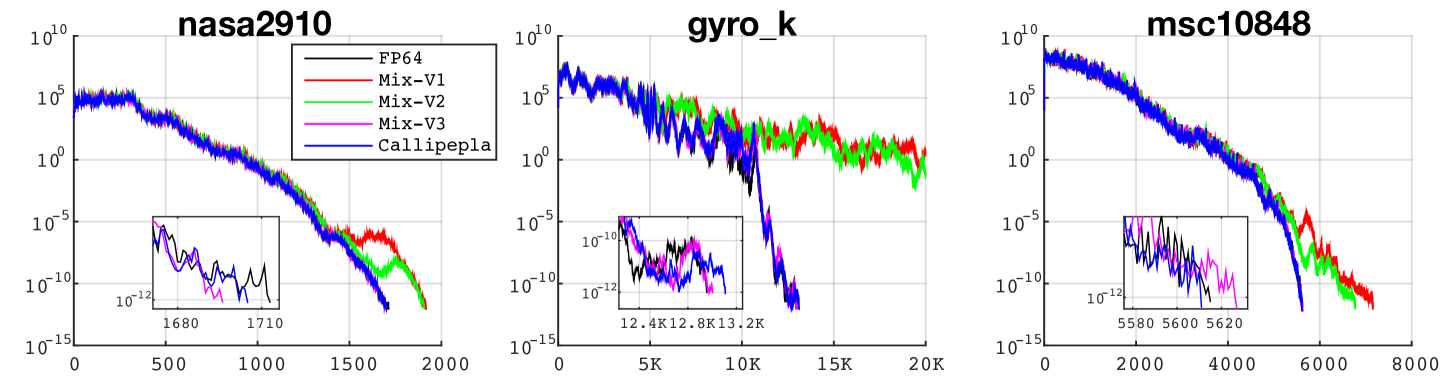
Figure 9 illustrates the residual traces of three matrices nasa2910, gyro_k, and msc10848 with default FP64, Mix-V1/V2/V3 precision settings and the residual traces from Callipepla on-board execution. From the residual trace of gyro_k we see that Mix-V1 (where all values are in FP32, colored in red) and Mix-V2 (where the SpMV input sparse matrix and input vector are in FP32, colored in green) do not converge within 20K iterations. All the three residual traces show the Mix-V3 (where only the SpMV input sparse matrix are in FP32, colored in magenta) are closely following the traces of the default CPU FP64 (colored in black). Although Callipepla employs the Mix-V3 precision, there is a small difference of the trace from Callipepla on-board execution (colored in blue) and the Mix-V3 trace. That is because the difference in hardware implementations of the CPU FP64 processing and the FPGA FP64 processing.
7.6. Bottleneck and Possible Improvement
In the design of Callipepla accelerator, we match the processing rate with the HBM bandwidth as discussed in Section 4. Therefore, the bottleneck of Callipepla is the HBM bandwidth. Exhibited in Table 2 the bandwidth of the NVIDIA A100 GPU is of Callipepla (1.56 TB/s v.s. 374 GB/s). There are two HBM stacks on a Xilinx U280 FPGA for a total bandwidth of 460 GB/s. If Xilinx deploys 8 () HBM stacks on a next generation HBM FPGA, we are able to achieve throughput advantage compared to an A100 GPU. However, the current HBM controllers is area-hungry. In our evaluation, the HBM controllers consume almost one SLR and a U280 FPGA only has 3 SLRs. It is not practical to scale up bandwidth with the current HBM controllers because that will consume 4 SLRs. We would like Xilinx to optimize the HBM controller IP or deploy it as an ASIC unit.
8. Conclusion
In the design of FPGA JPCG accelerator we overcome three challenges – (1) the support an arbitrary problem and accelerator termination on the fly, (2) the coordination of long-vector data flow among processing modules, and (3) saving off-chip memory bandwidth and maintaining FP64 precision convergence. To resolve the challenges, we present Callipepla, an CG accelerator on Xilinx U280 HBM FPGAs with our innovative solutions – (1) a stream centric instruction set, (2) vector streaming reuse and decentralized vector scheduling, and (3) mixed FP32/FP64 precision SpMV. The evaluation shows that compared to the Xilinx HPC product XcgSolver, Callipepla achieves a speedup of , higher throughput, and better energy efficiency. We also achieve 77% of the throughput with higher energy efficiency compared with an NVIDIA A100 GPU.
ACKNOWLEDGEMENTS
We thank the anonymous reviewers of FPGA 2023 for their constructive comments and Jinming Zhuang for helping with the artifact evaluation. This work is supported in part by the NSF RTML Program (CCF-1937599), CDSC industrial partners (https://cdsc.ucla.edu/partners), the Xilinx XACC Program, and the AMD222J. Cong has a finacial interest in AMD. HACC Program.
References
- (1)
- Antoulas (2005) Athanasios C Antoulas. 2005. Approximation of Large-Scale Dynamical Systems. Vol. 6. SIAM.
- Cheng et al. (2020) Jianyi Cheng, Lana Josipovic, George A Constantinides, Paolo Ienne, and John Wickerson. 2020. Combining Dynamic & Static Scheduling in High-level Synthesis. In Proceedings of the 2020 ACM/SIGDA International Symposium on Field-Programmable Gate Arrays. 288–298.
- Cheng et al. (2021) Jianyi Cheng, Lana Josipović, George A Constantinides, Paolo Ienne, and John Wickerson. 2021. DASS: Combining Dynamic & Static Scheduling in High-Level Synthesis. IEEE Transactions on Computer-Aided Design of Integrated Circuits and Systems 41, 3 (2021), 628–641.
- Chi and Cong (2020) Yuze Chi and Jason Cong. 2020. Exploiting Computation Reuse for Stencil Accelerators. In 2020 57th ACM/IEEE Design Automation Conference (DAC). IEEE, 1–6.
- Chi et al. (2018) Yuze Chi, Jason Cong, Peng Wei, and Peipei Zhou. 2018. SODA: Stencil with Optimized Dataflow Architecture. In 2018 IEEE/ACM International Conference on Computer-Aided Design (ICCAD). IEEE, 1–8.
- Chi et al. (2021) Yuze Chi, Licheng Guo, Jason Lau, Young-kyu Choi, Jie Wang, and Jason Cong. 2021. Extending High-Level Synthesis for Task-Parallel Programs. In 2021 IEEE 29th Annual International Symposium on Field-Programmable Custom Computing Machines (FCCM). IEEE, 204–213.
- Choi et al. (2021) Young-kyu Choi, Yuze Chi, Weikang Qiao, Nikola Samardzic, and Jason Cong. 2021. HBM Connect: High-Performance HLS Interconnect for FPGA HBM. In The 2021 ACM/SIGDA International Symposium on Field-Programmable Gate Arrays. 116–126.
- Cong et al. (2018) Jason Cong, Zhenman Fang, Yuchen Hao, Peng Wei, Cody Hao Yu, Chen Zhang, and Peipei Zhou. 2018. Best-Effort FPGA Programming: A Few Steps Can Go a Long Way. arXiv preprint arXiv:1807.01340 (2018).
- Cong et al. (2014) Jason Cong, Muhuan Huang, and Peng Zhang. 2014. Combining Computation and Communication Optimizations in System Synthesis for Streaming Applications. In Proceedings of the 2014 ACM/SIGDA international symposium on Field-programmable gate arrays. 213–222.
- Cong and Wang (2018) Jason Cong and Jie Wang. 2018. PolySA: Polyhedral-Based Systolic Array Auto-Compilation. In 2018 IEEE/ACM International Conference on Computer-Aided Design (ICCAD). IEEE, 1–8.
- Davis and Hu (2011) Timothy A. Davis and Yifan Hu. 2011. The University of Florida Sparse Matrix Collection. ACM Transactions on Mathematical Software (TOMS) 38, 1 (2011), 1–25.
- Dongarra et al. (2015) Jack Dongarra, Michael A Heroux, and Piotr Luszczek. 2015. HPCG Benchmark: A New Metric for Ranking High Performance Computing Systems. Knoxville, Tennessee 42 (2015). https://hpcg-benchmark.org/custom/index.html?lid=155&slid=313
- Ferziger and Perić (2002) Joel H Ferziger and Milovan Perić. 2002. Computational Methods for Fluid Dynamics. Vol. 3. Springer.
- Fowers et al. (2014) Jeremy Fowers, Kalin Ovtcharov, Karin Strauss, Eric S. Chung, and Greg Stitt. 2014. A High Memory Bandwidth FPGA Accelerator for Sparse Matrix-Vector Multiplication. In 2014 IEEE 22nd Annual International Symposium on Field-Programmable Custom Computing Machines. IEEE, 36–43.
- Griewank and Walther (2008) Andreas Griewank and Andrea Walther. 2008. Evaluating Derivatives: Principles and Techniques of Algorithmic Differentiation. Vol. 105. SIAM.
- Guo et al. (2022) Licheng Guo, Yuze Chi, Jason Lau, Linghao Song, Xingyu Tian, Moazin Khatti, Weikang Qiao, Jie Wang, Ecenur Ustun, Zhenman Fang, et al. 2022. TAPA: A Scalable Task-Parallel Dataflow Programming Framework for Modern FPGAs with Co-Optimization of HLS and Physical Design. arXiv preprint arXiv:2209.02663 (2022).
- Guo et al. (2021) Licheng Guo, Yuze Chi, Jie Wang, Jason Lau, Weikang Qiao, Ecenur Ustun, Zhiru Zhang, and Jason Cong. 2021. AutoBridge: Coupling Coarse-Grained Floorplanning and Pipelining for High-Frequency HLS Design on Multi-Die FPGAs. In The 2021 ACM/SIGDA International Symposium on Field-Programmable Gate Arrays. 81–92.
- Guo et al. (2020) Licheng Guo, Jason Lau, Yuze Chi, Jie Wang, Cody Hao Yu, Zhe Chen, Zhiru Zhang, and Jason Cong. 2020. Analysis and Optimization of the Implicit Broadcasts in FPGA HLS to Improve Maximum Frequency. In 2020 57th ACM/IEEE Design Automation Conference (DAC). IEEE, 1–6.
- Guo et al. (2019) Licheng Guo, Jason Lau, Zhenyuan Ruan, Peng Wei, and Jason Cong. 2019. Hardware Acceleration of Long Read Pairwise Overlapping in Genome Sequencing: A Race Between FPGA and GPU. In 2019 IEEE 27th Annual International Symposium on Field-Programmable Custom Computing Machines (FCCM). IEEE, 127–135.
- Helfenstein and Koko (2012) Rudi Helfenstein and Jonas Koko. 2012. Parallel Preconditioned Conjugate Gradient Algorithm on GPU. J. Comput. Appl. Math. 236, 15 (2012), 3584–3590.
- Hestenes and Stiefel (1952) Magnus R Hestenes and Eduard Stiefel. 1952. Methods of Conjugate Gradients for Solving Linear Systems. J. Res. Nat. Bur. Standards 49, 6 (1952), 409.
- Higham and Mary (2022) Nicholas J Higham and Théo Mary. 2022. Mixed Precision Algorithms in Numerical Linear Algebra. Acta Numerica 31 (2022), 347–414.
- Hu et al. (2021) Yuwei Hu, Yixiao Du, Ecenur Ustun, and Zhiru Zhang. 2021. GraphLily: Accelerating Graph Linear Algebra on HBM-Equipped FPGAs. In 2021 IEEE/ACM International Conference on Computer-Aided Design (ICCAD). IEEE, 1–9.
- Kershaw (1978) David S Kershaw. 1978. The Incomplete Cholesky—Conjugate Gradient Method for the Iterative Solution of Systems of Linear Equations. J. Comput. Phys. 26, 1 (1978), 43–65.
- Liu et al. (2022) Sihao Liu, Jian Weng, Dylan Kupsh, Atefeh Sohrabizadeh, Zhengrong Wang, Licheng Guo, Jiuyang Liu, Maxim Zhulin, Rishabh Mani, Lucheng Zhang, et al. 2022. OverGen: Improving FPGA Usability through Domain-specific Overlay Generation. In 2022 55th IEEE/ACM International Symposium on Microarchitecture (MICRO). IEEE, 35–56.
- Lopes and Constantinides (2008) Antonio Roldao Lopes and George A Constantinides. 2008. A High Throughput FPGA-Based Floating Point Conjugate Gradient Implementation. In International Workshop on Applied Reconfigurable Computing. Springer, 75–86.
- Maslennikow et al. (2005) Oleg Maslennikow, Volodymyr Lepekha, and Anatoli Sergyienko. 2005. FPGA Implementation of the Conjugate Gradient Method. In International Conference on Parallel Processing and Applied Mathematics. Springer, 526–533.
- Nakano (1997) Aiichiro Nakano. 1997. Parallel Multilevel Preconditioned Conjugate-gradient Approach to Variable-Charge Molecular Dynamics. Computer Physics Communications 104, 1-3 (1997), 59–69.
- Nowatzki et al. (2018) Tony Nowatzki, Newsha Ardalani, Karthikeyan Sankaralingam, and Jian Weng. 2018. Hybrid Optimization/Heuristic Instruction Scheduling for Programmable Accelerator Codesign. In Proceedings of the 27th International Conference on Parallel Architectures and Compilation Techniques. 1–15.
- Nowatzki et al. (2017) Tony Nowatzki, Vinay Gangadhar, Newsha Ardalani, and Karthikeyan Sankaralingam. 2017. Stream-Dataflow Acceleration. In 2017 ACM/IEEE 44th Annual International Symposium on Computer Architecture (ISCA). IEEE, 416–429.
- NVIDIA (2021) NVIDIA. 2021. NVIDIA A100 TENSOR CORE GPU. https://www.nvidia.com/content/dam/en-zz/Solutions/Data-Center/a100/pdf/a100-80gb-datasheet-update-nvidia-us-1521051-r2-web.pdf.
- Rampalli et al. (2018) Sahithi Rampalli, Natasha Sehgal, Ishita Bindlish, Tanya Tyagi, and Pawan Kumar. 2018. Efficient FPGA Implementation of Conjugate Gradient Methods for Laplacian System using HLS. arXiv preprint arXiv:1803.03797 (2018).
- Roldao-Lopes et al. (2009) Antonio Roldao-Lopes, Amir Shahzad, George A Constantinides, and Eric C Kerrigan. 2009. More Flops or More Precision? Accuracy Parameterizable Linear Equation Solvers for Model Predictive Control. In 2009 17th IEEE Symposium on Field Programmable Custom Computing Machines. IEEE, 209–216.
- Saad (2003) Yousef Saad. 2003. Iterative Methods for Sparse Linear Systems. Society for Industrial and Applied Mathematics.
- Sohrabizadeh et al. (2020) Atefeh Sohrabizadeh, Jie Wang, and Jason Cong. 2020. End-to-End Optimization of Deep Learning Applications. In Proceedings of the 2020 ACM/SIGDA International Symposium on Field-Programmable Gate Arrays. 133–139.
- Song et al. (2020) Linghao Song, Fan Chen, Xuehai Qian, Hai Li, and Yiran Chen. 2020. Low-Cost Floating-Point Processing in ReRAM for Scientific Computing. arXiv preprint arXiv:2011.03190 (2020).
- Song et al. (2022a) Linghao Song, Yuze Chi, Licheng Guo, and Jason Cong. 2022a. Serpens: A High Bandwidth Memory Based Accelerator for General-Purpose Sparse Matrix-Vector Multiplication. In Proceedings of the 59th ACM/IEEE Design Automation Conference. 211–216.
- Song et al. (2022b) Linghao Song, Yuze Chi, Atefeh Sohrabizadeh, Young-kyu Choi, Jason Lau, and Jason Cong. 2022b. Sextans: A Streaming Accelerator for General-Purpose Sparse-Matrix Dense-Matrix Multiplication. In Proceedings of the 2022 ACM/SIGDA International Symposium on Field-Programmable Gate Arrays. 65–77.
- Song et al. (2018) Linghao Song, Youwei Zhuo, Xuehai Qian, Hai Li, and Yiran Chen. 2018. GraphR: Accelerating Graph Processing Using ReRAM. In 2018 IEEE International Symposium on High Performance Computer Architecture (HPCA). IEEE, 531–543.
- Technology (2022) Livermore Software Technology. 2022. LS-DYNA. https://www.lstc.com/products/ls-dyna
- Wang et al. (2021) Jie Wang, Licheng Guo, and Jason Cong. 2021. AutoSA: A Polyhedral Compiler for High-Performance Systolic Arrays on FPGA. In The 2021 ACM/SIGDA International Symposium on Field-Programmable Gate Arrays. 93–104.
- Weng et al. (2020a) Jian Weng, Sihao Liu, Vidushi Dadu, Zhengrong Wang, Preyas Shah, and Tony Nowatzki. 2020a. DSAGEN: Synthesizing Programmable Spatial Accelerators. In 2020 ACM/IEEE 47th Annual International Symposium on Computer Architecture (ISCA). IEEE, 268–281.
- Weng et al. (2022) Jian Weng, Sihao Liu, Dylan Kupsh, and Tony Nowatzki. 2022. Unifying Spatial Accelerator Compilation with Idiomatic and Modular Transformations. IEEE Micro 42, 5 (2022), 59–69.
- Weng et al. (2020b) Jian Weng, Sihao Liu, Zhengrong Wang, Vidushi Dadu, and Tony Nowatzki. 2020b. A Hybrid Systolic-Dataflow Architecture for Inductive Matrix Algorithms. In 2020 IEEE International Symposium on High Performance Computer Architecture (HPCA). IEEE, 703–716.
- Xilinx (2022a) Xilinx. 2022a. Alveo U280 Data Center Accelerator Card Data Sheet. https://www.xilinx.com/content/dam/xilinx/support/documents/data_sheets/ds963-u280.pdf.
- Xilinx (2022b) Xilinx. 2022b. Vitis HPC Library. https://xilinx.github.io/Vitis_Libraries/hpc/2022.1/index.html
- Xilinx (2022c) Xilinx. 2022c. Vitis Libraries. https://github.com/Xilinx/Vitis_Libraries
- Zeng and Prasanna (2020) Hanqing Zeng and Viktor Prasanna. 2020. GraphACT: Accelerating GCN training on CPU-FPGA heterogeneous platforms. In Proceedings of the 2020 ACM/SIGDA International Symposium on Field-Programmable Gate Arrays. 255–265.
- Zhang et al. (2015) Chen Zhang, Peng Li, Guangyu Sun, Yijin Guan, Bingjun Xiao, and Jason Cong. 2015. Optimizing FPGA-based Accelerator Design for Deep Convolutional Neural Networks. In Proceedings of the 2015 ACM/SIGDA International Symposium on Field-Programmable Gate Arrays. 161–170.
- Zhao et al. (2017) Ritchie Zhao, Weinan Song, Wentao Zhang, Tianwei Xing, Jeng-Hau Lin, Mani Srivastava, Rajesh Gupta, and Zhiru Zhang. 2017. Accelerating Binarized Convolutional Neural Networks with Software-Programmable FPGAs. In Proceedings of the 2017 ACM/SIGDA International Symposium on Field-Programmable Gate Arrays. 15–24.