Direct laser written aperiodic photonic volume elements for complex light shaping with high efficiency: inverse design and fabrication
Abstract
Light plays the central role in many applications. The key to unlocking its versatility lies in shaping it into the most appropriate form for the task at hand. Specifically tailored refractive index modifications, directly manufactured inside glass using a short pulsed laser, enable an almost arbitrary control of the light flow. However, the stringent requirements for quantitative knowledge of these modifications, as well as for fabrication precision, have so far prevented the fabrication of light-efficient aperiodic photonic volume elements (APVEs).
Here we present a powerful approach to the design and manufacturing of light-efficient APVEs. We optimize application-specific 3D arrangements of hundred thousands of microscopic voxels and manufacture them using femtosecond direct laser writing inside millimeter-sized glass volumes. We experimentally achieve unprecedented diffraction efficiencies up to 80%, which is enabled by precise voxel characterization and adaptive optics during fabrication.
We demonstrate APVEs with various functionalities, including a spatial mode converter and combined intensity shaping and wavelength-multiplexing. Our elements can be freely designed and are efficient, compact and robust. Our approach is not limited to borosilicate glass, but is potentially extendable to other substrates, including birefringent and nonlinear materials, giving a preview of even broader functionalities including polarization modulation and dynamic elements.
1 Introduction
Light has become an indispensable tool in our modern day societies. It plays the central role in countless technological solutions, such as in the information transport along glass fibers or in various display, imaging and sensing applications [1]. The increasing significance of light as a tool sparked a sharply rising demand of technologies that enable the temporal and spatial sculpting of light in user-defined ways [2, 3, 4].
Of notable importance are so-called multiplexing applications, where one of many pre-defined output fields can be created upon presenting a unique pre-defined input field. Elements that can handle such tasks with high efficiency would find numerous applications in the analysis and synthesis of light fields. Examples range from conventional spectroscopy to complex tasks around information processing and transport. Mode-division multiplexing for example is a potential solution for avoiding the threat of reaching an upper limit in communication speed (“capacity crunch”) [5, 6, 7, 8]. Meanwhile optical computing is currently experiencing a revival thanks to novel ways of manufacturing computer-designed optical networks which enable sophisticated data processing at the speed of light [9, 10, 11, 12, 13].
Optically recorded volume holograms, e.g. from photorefractive materials [14], have traditionally been used for multiplexing applications [15, 16]. However, creating such holograms requires the realization of matching physical interference patterns at the recording step, and the approach is also limited to photosensitive substrates, which severely limits its practical applicability.
Aperiodic Photonic Volume Elements (APVE) can circumvent these limitations: they are designed on the computer and open to a multitude of different manufacturing techniques. For instance, they can be directly written into a substrate by locally changing its 3D refractive index (RI) distribution in a voxel by voxel fashion. However, a major challenge in the production of APVEs is to meet the high accuracy requirements for manufacturing since producing an efficient APVE puts high demands on the ability to modify the 3D RI distribution with high precision. Since the output light field arises from the interference of thousands of scattered waves, even small errors made on the voxel-scale quickly accumulate and severely degrade the output field quality. For this reason, past demonstrations of manufacturing APVEs in glass have been limited to proof of concept studies with rather low diffraction efficiencies [17] or restricted to 2D configurations [18]. Recently, 2-photon polymerization additive manufacturing of multi-layer holograms [9] and the fabrication of 3D graded index materials [10] have been demonstrated.
Here we introduce a novel approach for realizing APVEs using direct laser writing in transparent dielectric media such as glass. Our method allows for obtaining high diffraction efficiencies of up to 80%, many times more than what could previously be achieved [17]. This is made possible by employing precise tomographic voxel characterization [19] in combination with a design algorithm based on numerical beam propagation and the use of adaptive optics to ensure space invariant voxel shapes throughout the full body of the APVE. We experimentally demonstrate the design and manufacture of three different, highly integrated APVEs that are optimized for intensity shaping, spatial mode and wavelength multiplexing.
We believe that our results represent an important step towards the realization of robust and highly integrated 3D light shapers for many important application fields, such as information transport [8], optical computing [9, 10, 11, 12, 13], the imaging through multimode fibers [20] and nonlinear photonics [21]. They may further help to obtain fundamental insights in the behaviour of quantum states of light upon scattering [22].
2 APVE concept
Figure 1 (a) illustrates the basic concept of our photonic volume element, which is a laser processed 3D region inside a glass substrate, containing hundreds of thousands of spatially separated voxels of modified refractive index at pre-defined positions. Our approach is based on past demonstrations of direct laser written aperiodic volume optics [17], but also inspired by previous work on computer-generated 2D holograms based on waveguides [23].
A single voxel measures only 1.757.510 µm3 and is created by moving the z-stage (the long horizontal axis) for 10 µm during exposure to the laser focus. Fabrication of the whole device takes about 20 minutes. The quantitative RI profile of a single voxel across the x-y-axes, fabricated in Eagle glass, is shown in (b). This profile must be precisely known, as it serves as the basis for the numerical design process. The RI profile characterization is performed in a home-build tomographic microscope [19]. The RI distribution of each voxel is assumed to be invariant along the z-direction. The input and output fields of the APVE are coupled through its smallest end facets. A widefield transmission image of a fabricated APVE is shown in (c).
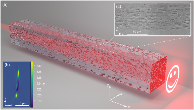
Our design algorithm operates on a Cartesian grid of size , following the directions of the coordinate system sketched in (a), which defines potential voxel positions. For our demonstrators, , and depending on the device extension along the propagation direction . This corresponds to a maximum number of voxels varying between 154,000 and 308,000. The number of voxels in the transverse - and -directions are quite different due to the elongated nature of our reference voxel represented in (b). Basically, the algorithm simulates the light flow through the device using a beam propagation method [24] and decides upon the activation of a voxel, depending on whether it would improve the output wavefront or not. For our experimental demonstration, we explored only binary designs made of identical voxels depicted in (b), but the inverse design algorithm we implemented generalizes well to multilevel RI modifications. Details about this algorithm are provided in the Appendix F.
The successful implementation of our APVE requires not only precise knowledge about the voxel properties, but also the manufacturing abilities to produce the same profile reliably at all targeted substrate depths. This can be ensured using dynamic wavefront control, which compensates for spherical aberrations arising when focusing the laser into the substrate [25]. Further information about the manufacturing is also provided in Appendix E.
3 Results
In the following, we explore three types of APVEs, designed for specific applications with different levels of complexity. The first one is a single-mode intensity shaper with a length of only 2 mm and discussed in section 3.1, the second one is a multi-colour (RGB) multiplexer of 3 mm length and discussed in section 3.2. Finally, a Hermite–Gaussian 6-mode sorter of 4 mm length is discussed in section 3.3.
3.1 Sculpting intensity distributions
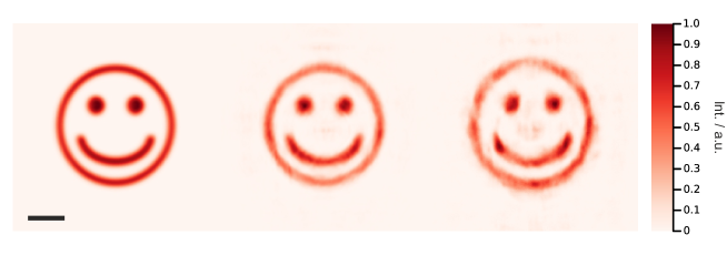
Our APVEs can be optimized to shape user-defined intensity patterns with high efficiency. To demonstrate this, we designed and fabricated an element producing a microscopic “smiley” at its output facet (i.e. the last layer of voxels) when read out with a Gaussian beam at zero degree readout angle (vacuum wavelength = 640 nm, waist = 40 µm). The physical dimensions of the element are 0.10.12 mm3 and it contains 55 14 200 voxels. As mentioned earlier, the unequal grid sizes along the - and -directions are due to the anisotropic voxel shape, which is a consequence of the likewise anisotropic shape of the focus creating the voxel. The device itself, i.e., the 3D region containing fabricated voxels, is embedded inside a larger glass chip for easier handling.
Figure 2 provides results obtained with this APVE. It shows the designed output intensity template for a Gaussian input of 40 µm waist as well as the simulated and experimentally obtained results. The simulated result was obtained by numerical propagation of the input beam through a computer model of the optimized voxel arrangement. It thus marks an upper limit for the quality achievable in the experiment. The experimental result was obtained by imaging the output plane with a regular widefield microscope (see Appendix B for additional information about the experimental APVE characterization).
The diffraction efficiency of the APVE has been determined by calculating an overlap integral of the target amplitude pattern with the simulated and experimentally measured output amplitude patterns over the area of the observable end facet :
| (1) |
where the powers of and are both normalized to 1. We introduce another efficiency metric , which further takes into account scattering losses into non-observable angles:
| (2) |
with transmission factor . Therefore, quantifies the power fraction of the measurable output light111the light arriving at the (simulated or real) camera plane which is effectively turned into the target distribution, while is the respective conversion efficiency for the input beam. Losses due to Fresnel reflections at the input/output facets of the APVE are neglected in this consideration.
The theoretical and experimental diffraction efficiencies of the smiley converter are 90% and 80%, respectively. We note that 1 for the smiley shaper in both simulation and experiment, i.e., the amount of scattering losses are close to zero. Since this application aims at intensity-only shaping, the phase distributions of and are irrelevant and thus assumed to be flat in Eq. 1. We further derived an error metric , defined as the root mean square (RMS) difference between normalized target and simulated/experimental output intensities. We find .
Therefore, even though the intensity shaping shown here can be easily achieved using 2D diffractive optical elements, we are nevertheless able to simply demonstrate that our computational design approach can be faithfully implemented through the experimental characterization and reproducible manufacture of 3D voxel arrangements inside glass.
3.2 Wavelength multiplexing
We demonstrate the feasibility of colour multiplexing by designing and fabricating a multi-colour “smiley” shaper, where different parts of the smiley (eyes, mouth, head) appear only for specific readout wavelengths as illustrated in Fig. 3. This APVE measures 0.10.13 mm3 and contains 55 14 300 voxels. When read out at 640 nm with a beam waist of = 40 µm, only the circular head appears at the output. Similarly, the eyes appear for a readout wavelength of 543 nm ( = 30 µm) and the mouth for 455 nm ( = 20 µm). Results obtained from simulated readouts and experiments using fiber-coupled lasers (see Appendix C for details) are summarized in Fig. 3. The image table depicts false-colour intensity distributions at the output facet of the APVE, which are individually normalized to their respective peak intensities. The fourth image column on the right shows a computer-generated overlap of the three readouts.
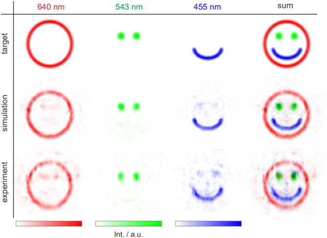
The simulated and experimentally determined power conversion efficiencies from the three Gaussian input beams to the respective facial structures are summarized in table 1. The table values are calculated using Eq. 1, i.e., they show which percentage of the output laser power is shaped into the respective facial structures. The average simulated efficiency over all colours is 67% for the simulation and 55% in the experiment. From the table values it is noticeable that in particular the blue wavelength shows the largest disparity between simulation and experiment, with an efficiency of 64% in the simulation and 49% in the experiment. This may be attributed to small remaining differences between the assumed and real voxel profiles at length scales of a few hundred nanometres. Such small irregularities will especially affect shorter wavelengths and are likely to be overlooked by our tomographic voxel characterization method, which employs the same wavelength for inspection and a smoothing total variation norm regularizer [19]. The simulated and experimentally measured transmission values for all three readout wavelengths are shown in table 2. We observe well matching numbers between simulation and experiment for the red and green wavelengths, while the blue transmission value is around 25% lower in the experiment than predicted by the simulation.
| head | eyes | mouth | |
|---|---|---|---|
| 640 | 77 | 2 | 1 |
| 543 | 8 | 60 | 7 |
| 455 | 3 | 7 | 64 |
| head | eyes | mouth | |
|---|---|---|---|
| 640 | 65 | 7 | 6 |
| 543 | 5 | 50 | 6 |
| 455 | 1 | 4 | 49 |
| 640 nm | 543 nm | 455 nm | |
|---|---|---|---|
| (head) | (eyes) | (mouth) | |
| T (sim) | 83 | 82 | 87 |
| T (exp) | 84 | 82 | 66 |
The simulated (experimental) total efficiencies for the head, eyes and mouth features are therefore 64% (55%), 49 (41%) and 56% (32%).
We further investigated the wavelength-dependent APVE properties using a fiber-coupled monochromator (Polychrome IV from TILL Photonics), whose output wavelength was tuned from 420 nm to 680 nm in steps of 10 nm. In contrast to the laser readouts where each beam had an individual, optimal waist value, the beam waist of the monochromator light at the APVE input facet was about 30 µm for all wavelengths (details are described in Appendix C). While this means that the monochromator results are expected to be somewhat sub-optimal they nevertheless provide valuable information about the wavelength dependence of the APVE.
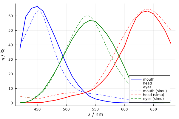
At each wavelength we took images of the input beam and the APVE output (see data in Appendix C), which allowed us to calculate wavelength dependent power conversion efficiencies according to Eq. 1 for each spatial feature (mouth, eyes, head). These efficiencies are plotted in Fig. 4. Of note, the peaks appear at wavelengths which almost exactly match the targets at 455 nm, 543 nm and 640 nm. The measured efficiencies at these wavelengths are 63%, 57% and 63% and thus close to the simulation values obtained from the laser readouts as shown in table 1 (left). Interestingly, the blue monochromator image of the "mouth" shows a significantly higher efficiency than the respective experimental blue laser readout (63% vs. 49%).
Figure 4 further contains data from simulated readouts (dashed lines), which resemble the experimental data. To match the experimental conditions, these simulations assumed a beam waist of 30 µm for all readout wavelengths, which cause the peak efficiency values to be slightly lower than the values in table 1, which assume readouts taken at the designed waist values.
3.3 Angular multiplexing
The high angular selectivity of a photonic volume element allows for encoding different outputs for varying input angles. This characteristic makes APVEs highly interesting for tasks such as mode division multiplexing and sorting. To investigate the feasibility of angular multiplexing for our approach, we have designed a APVE measuring only 0.10.14 mm3 and containing 55 14 400 voxels, which produces different Hermite-Gaussian (HG) modes depending on the angle of incidence (AOI) of a Gaussian readout beam.
Such a device could be used as a mode division multiplexer to enhance data transfer speed as sketched in Fig. 5: multiple signals are delivered by single mode fibers in a triangular arrangement, which has been shown to facilitate high Hermite-Gaussian (HG) mode conversion efficiencies [26]. The fiber ends are in the focal plane of a convex lens, which collimates the light leaving the fiber outputs and sends it into the APVE at different, fiber-specific propagation angles. The APVE converts each signal into a particular HG mode travelling in parallel to the optical axis, such that it can be efficiently coupled into a single multimode fiber.
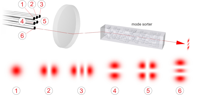
We designed a mode sorting APVE for readout with a Gaussian input of 640 nm wavelength and 25 µm waist. Altering the input beam’s AOI by merely 1.4 degrees (defined in air) transforms the output field from one particular Hermite-Gaussian (HG) mode to another. In total we encode six different HG modes as shown in Fig. 5.
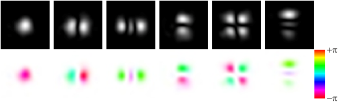
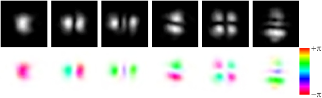
Figure 6 shows the output intensities and phases resulting from a simulated readout of the mode sorting APVE. The matching experimental data are shown in Fig. 7. For both, simulation and experiment, the numerical aperture (NA) at the output needs to be reduced in order to block stray light produced by the element. This reduces the overall light efficiency but enhances the quality of the generated modes. In simulation the NA was restricted to 0.02, in experiment to about 0.05.
As for the APVEs discussed previously, the overall quality of the mode sorter is governed by two factors: (i) the purity of the generated modes and (ii) the transmission of the APVE quantified by parameter . Although the element itself absorbs almost no light, there is some power loss caused by the aperture stop restricting the imaging NA. We quantified point (i) by calculating efficiency values in analogy to Eq. 1 and taking the different HG modes as target fields:
| (3) |
where and represent the target mode and conjugate output field with their total powers normalized to 1. An efficiency value of means that the field has been shaped into a perfect mode, whereas means that the field is orthogonal to this mode. Tables 3 and 4 contain efficiency values of the simulated and experimental mode sorter. The off-diagonal terms represent undesired crosstalks into neighbouring channels. The purest modes have efficiency values of 90% in the simulation and 88% in the experiment. The highest crosstalk values are 3% for the simulation and 5% for the experiment.
The mode-dependent transmission of the APVE (ii), including both losses due to scattering and spatial filtering by the restricted imaging NA, are summarized in table 5. These results are still far from what could be theoretically obtained with a gradient index design [27], but they are surprisingly good for a binary design. Introducing different types of voxels as new degrees of freedom for the inverse design optimization could significantly improve the capabilities of these mode multiplexers and approach the maximum performance of gradient index designs, for which a mature manufacturing technology is not yet available in glass.
| input angle no. | HG00 | HG10 | HG20 | HG01 | HG11 | HG02 |
|---|---|---|---|---|---|---|
| 1 | 90.6 | |||||
| 2 | 89.1 | |||||
| 3 | 90.2 | |||||
| 4 | 87.2 | |||||
| 5 | 93.9 | |||||
| 6 | 79.6 |
| input angle no. | HG00 | HG10 | HG20 | HG01 | HG11 | HG02 |
|---|---|---|---|---|---|---|
| 1 | 88.4 | |||||
| 2 | 87.0 | |||||
| 3 | 83.8 | |||||
| 4 | 83.7 | |||||
| 5 | 86.6 | |||||
| 6 | 65.7 |
| HG00 | HG10 | HG20 | HG01 | HG11 | HG02 | |
|---|---|---|---|---|---|---|
| T (sim) | ||||||
| T (exp) |
4 Discussion
In this discussion section, we place our method in the context of related technological approaches.
Optically recorded volume holograms
An important difference between traditional volume holograms and our APVEs exists in the physics of their creation. Traditional holograms are optically recorded by transferring the properties of interference patterns into a photosensitive material, such as a photopolymer [28, 29] or a photorefractive crystal [30], which comes naturally with limitations. Firstly, each desired function must be physically realized at the recording step, which becomes unfeasible for advanced multiplexing applications. Secondly, one is bound to a limited number of suitable photosensitive materials. Finally, the dynamic range of optically recorded holograms is quickly consumed by only a few multiplexed recordings, which has an adverse effect on the obtainable diffraction efficiency [10].
Meta-holograms
In contrast to the APVE concept presented here, meta-holograms rely on nanostructured metallic or dielectric surfaces, on which “meta-atoms” interact with light in pre-defined ways [31, 32, 33, 34]. While the concept has proven to be especially powerful for wavelength and polarization-multiplexing tasks, angular multiplexing, i.e., the generation of different output fields at varying input angles, appears harder to achieve: only up to four multiplexed fields could be generated upon a large angular variation of more then 60 deg. [35]. Some folded multiplane designs using metasurfaces have been realized recently in order to increase the multiplexing capabilities of these meta-holograms [36]. Yet, the advantages of using metasurfaces in this context seems limited since 3 reflections are required to achieve only a 3-mode sorter, which is not significantly better than what more conventional cascaded diffractive optical elements can provide [9].
Silicon Photonics
The field of silicon photonics [37, 38], i.e., the manufacturing and use of photonic integrated circuits (PICs) inside silicon, is attracting considerable attention since more than a decade. The fabrication of photonic chips can rely on existing infrastructure and lithographic techniques used in the electronic semiconductor industry and enables structure sizes down to a few nanometres. The field of silicon photonics is comparably mature, the demonstration of wavelength multiplexing for instance dates back to the 1990s [39] and has been further developed towards high integration by employing modern tools of inverse design [40]. Spatial multimode operations have been developed later, but are likewise possible in a highly integrated fashion [41]. Compared to silicon photonics, which is bound to infrared wavelengths, our approach offers a wavelength window reaching down to the UV, depending on the substrate, and is potentially applicable to a larger variety of materials offering different optical properties, including electro-optical and nonlinear ones. Furthermore, glasses as substrate facilitate novel applications linking optical and microfluidic technologies [42] and allow for easier light coupling compared to silicon, where mode mismatch can cause important insertion losses [43]. Lastly, the manufacturing of 3D devices is more innate to direct laser writing than it is to standard lithographic techniques [44] and puts also lower demands on the required infrastructure (no clean room required).
Writing voxels for data storage
From the manufacturing point of view, our approach is related to storing data by writing of voxels inside polymers or glass [45, 46]. This application has already reached an impressive maturity level, employing birefringent multi-level voxels [47]. However, in contrast to our application, data storage applications put significantly lower demands on the knowledge about the quantitative 3D properties of a single voxel, as well as their reproducible and spatially invariant fabrication, since they can be read out sequentially and any slight deviation from the assumed voxel shape would be irrelevant since only a few Bits are encoded in a single voxel. Conversely, hundreds of thousands voxels act jointly on the readout light in our APVEs, such that even small systematic errors at the single voxel level would have pronounced adverse effects on the sculpted fields.
5 Conclusion and summary
We present a novel design and fabrication concept for robust and light efficient aperiodic photonic volume elements. Our design algorithm uses a mode-matching method and numerical beam propagation. The manufacturing is based on directly writing an optimized 3D arrangement of voxels into the volume of a transparent dielectric such as glass using a focused femtosecond laser. Each voxel consists of a small volume (approx. 1.757.510 µm3) of slightly increased RI. Precise knowledge of the properties of a single voxel, in conjunction with an advanced fabrication technique, allowed us to physically realize APVEs of high efficiencies up to 80%.
We experimentally realize three different APVE designs demonstrating different functionalities: An intensity shaper turning a Gaussian beam into a smiley-shaped light distribution, a wavelength multiplexer producing different parts of the smiley for three different readout wavelengths and a spatial mode multiplexer, which converts a Gaussian input beam into particular HG modes depending on the angle of incidence.
While our proof-of-concept studies already show unprecedented performance, our APVE concept still has room for improvement in several respects, promising significantly higher efficiency and more complex functionalities in the future. For instance, our APVEs are made from a single voxel type, i.e., they are binary devices. However, it is straightforward to extend the design concept to non-binary devices. At the manufacturing side the use of varying laser powers, focus shapes, or multi-pass writing could be used to fabricate multiple different RI profiles. Non-binary devices will be able to store more information and exhibit higher efficiencies. In addition, our concept is extensible to different types of substrates, including birefringent, electro-optic and nonlinear substrates, potentially offering the possibility of polarization shaping, dynamic or even erasable ferroelectric APVEs [48].
Acknowledgments
We thank Lisa Ackermann and Clemens Roider for valuable contributions in the form of scientific discussions as well as for post processing the APVE samples.
Funding
The work is funded by the FWF (I3984-N36), the EPSRC UK (R004803/01) and the DFG (409765270).
References
- [1] Thomas D. Rossing and Christopher J. Chiaverina. Photonics—Light in the Twenty-First Century, pages 333–355. Springer International Publishing, Cham, 2019.
- [2] Halina Rubinsztein-Dunlop, Andrew Forbes, M V Berry, M R Dennis, David L Andrews, Masud Mansuripur, Cornelia Denz, Christina Alpmann, Peter Banzer, Thomas Bauer, Ebrahim Karimi, Lorenzo Marrucci, Miles Padgett, Monika Ritsch-Marte, Natalia M Litchinitser, Nicholas P Bigelow, C Rosales-Guzmán, A Belmonte, J P Torres, Tyler W Neely, Mark Baker, Reuven Gordon, Alexander B Stilgoe, Jacquiline Romero, Andrew G White, Robert Fickler, Alan E Willner, Guodong Xie, Benjamin McMorran, and Andrew M Weiner. Roadmap on structured light. Journal of Optics, 19(1):013001, 2016.
- [3] Andrew Forbes, Michael de Oliveira, and Mark R Dennis. Structured light. Nature Photonics, 15(4):253–262, 2021.
- [4] Marco Piccardo, Vincent Ginis, Andrew Forbes, Simon Mahler, Asher A Friesem, Nir Davidson, Haoran Ren, Ahmed H Dorrah, Federico Capasso, Firehun T Dullo, Balpreet S Ahluwalia, Antonio Ambrosio, Sylvain Gigan, Nicolas Treps, Markus Hiekkamäki, Robert Fickler, Michael Kues, David Moss, Roberto Morandotti, Johann Riemensberger, Tobias J Kippenberg, Jérôme Faist, Giacomo Scalari, Nathalie Picqué, Theodor W Hänsch, Giulio Cerullo, Cristian Manzoni, Luigi A Lugiato, Massimo Brambilla, Lorenzo Columbo, Alessandra Gatti, Franco Prati, Abbas Shiri, Ayman F Abouraddy, Andrea Alù, Emanuele Galiffi, J B Pendry, and Paloma A Huidobro. Roadmap on multimode light shaping. Journal of Optics, 24(1):013001, 2021.
- [5] David J Richardson, John M Fini, and Lynn E Nelson. Space-division multiplexing in optical fibres. Nature Photonics, 7(5):354–362, 2013.
- [6] Guifang Li, Neng Bai, Ningbo Zhao, and Cen Xia. Space-division multiplexing: the next frontier in optical communication. Advances in Optics and Photonics, 6(4):413–487, 2014.
- [7] Peter J Winzer, David T Neilson, and Andrew R Chraplyvy. Fiber-optic transmission and networking: the previous 20 and the next 20 years. Optics Express, 26(18):24190–24239, 2018.
- [8] Benjamin J Puttnam, Georg Rademacher, and Ruben S Luís. Space-division multiplexing for optical fiber communications. Optica, 8(9):1186–1203, 2021.
- [9] Niyazi Ulas Dinc, Joowon Lim, Eirini Kakkava, Christophe Moser, and Demetri Psaltis. Computer generated optical volume elements by additive manufacturing. Nanophotonics, 9(13):4173–4181, 2020.
- [10] Xavier Porte, Niyazi Ulas Dinc, Johnny Moughames, Giulia Panusa, Caroline Juliano, Muamer Kadic, Christophe Moser, Daniel Brunner, and Demetri Psaltis. Direct (3+ 1) d laser writing of graded-index optical elements. Optica, 8(10):1281–1287, 2021.
- [11] Johnny Moughames, Xavier Porte, Michael Thiel, Gwenn Ulliac, Laurent Larger, Maxime Jacquot, Muamer Kadic, and Daniel Brunner. Three-dimensional waveguide interconnects for scalable integration of photonic neural networks. Optica, 7(6):640–646, 2020.
- [12] Yi Luo, Yifan Zhao, Jingxi Li, Ege Çetintaş, Yair Rivenson, Mona Jarrahi, and Aydogan Ozcan. Computational imaging without a computer: seeing through random diffusers at the speed of light. eLight, 2(1):1–16, 2022.
- [13] Kun Liao, Ye Chen, Zhongcheng Yu, Xiaoyong Hu, Xingyuan Wang, Cuicui Lu, Hongtao Lin, Qingyang Du, Juejun Hu, and Qihuang Gong. All-optical computing based on convolutional neural networks. Opto-Electronic Advances, 4(11):200060, 2021.
- [14] Peter Günter and Jean-Pierre Huignard. Photorefractive materials and their applications, volume 114. Springer, 2007.
- [15] Hans J Coufal, Demetri Psaltis, and Glenn T Sincerbox. Holographic data storage, volume 8. Springer, 2000.
- [16] Yuta Wakayama, Atsushi Okamoto, Kento Kawabata, Akihisa Tomita, and Kunihiro Sato. Mode demultiplexer using angularly multiplexed volume holograms. Optics Express, 21(10):12920–12933, 2013.
- [17] Tim D Gerke and Rafael Piestun. Aperiodic volume optics. Nature Photonics, 4(3):188–193, 2010.
- [18] Glen Douglass, W. Minster Kunkel, Ali Ghoreyshi, Simon Gross, Michael J. Withford, and James R. Leger. Two dimensional gradient-index beam shapers fabricated using ultrafast laser inscription. Optics Express, 30(22):40592–40598, Oct 2022.
- [19] Nicolas Barré, Ravi Shivaraman, Lisa Ackermann, Simon Moser, Michael Schmidt, Patrick Salter, Martin Booth, and Alexander Jesacher. Tomographic refractive index profiling of direct laser written waveguides. Optics Express, 29(22):35414–35425, 2021.
- [20] Unė G Būtaitė, Hlib Kupianskyi, Tomáš Čižmár, and David B Phillips. How to build the optical inverse of a multimode fibre. arXiv preprint arXiv:2204.02865, 2022.
- [21] Logan G. Wright, William H. Renninger, Demetri N. Christodoulides, and Frank W. Wise. Nonlinear multimode photonics: nonlinear optics with many degrees of freedom. Optica, 9(7):824–841, Jul 2022.
- [22] Ohad Lib and Yaron Bromberg. Quantum light in complex media and its applications. Nature Physics, 18(9):986–993, 2022.
- [23] René Berlich, Daniel Richter, Martin Richardson, and Stefan Nolte. Fabrication of computer-generated holograms using femtosecond laser direct writing. Optics Letters, 41(8):1752–1755, 2016.
- [24] MD Feit and JA Fleck. Light propagation in graded-index optical fibers. Applied Optics, 17(24):3990–3998, 1978.
- [25] Alexander Jesacher and Martin J Booth. Parallel direct laser writing in three dimensions with spatially dependent aberration correction. Optics Express, 18(20):21090–21099, 2010.
- [26] Nicolas K Fontaine, Roland Ryf, Haoshuo Chen, David T Neilson, Kwangwoong Kim, and Joel Carpenter. Laguerre-gaussian mode sorter. Nature Communications, 10(1):1–7, 2019.
- [27] Nicolas Barré and Alexander Jesacher. Inverse design of gradient-index volume multimode converters. Optics Express, 30(7):10573–10587, 2022.
- [28] WS Colburn and KA Haines. Volume hologram formation in photopolymer materials. Applied Optics, 10(7):1636–1641, 1971.
- [29] Jian Jialing, Cao Lin, Wei Xiqiao, Guo Jinxin, Wang Dayong, and Zhang Xinping. A review of photopolymers on holography volume data storage. Opto-Electronic Engineering, 46(3):180552–1, 2019.
- [30] Lambertus Hesselink, Sergei S Orlov, Alice Liu, Annapoorna Akella, David Lande, and Ratnakar R Neurgaonkar. Photorefractive materials for nonvolatile volume holographic data storage. Science, 282(5391):1089–1094, 1998.
- [31] Nanfang Yu and Federico Capasso. Flat optics with designer metasurfaces. Nature materials, 13(2):139–150, 2014.
- [32] Benny Walther, Christian Helgert, Carsten Rockstuhl, Frank Setzpfandt, Falk Eilenberger, Ernst-Bernhard Kley, Falk Lederer, Andreas Tünnermann, and Thomas Pertsch. Spatial and spectral light shaping with metamaterials. Advanced Materials, 24(47):6300–6304, 2012.
- [33] Jacob Scheuer. Metasurfaces-based holography and beam shaping: engineering the phase profile of light. Nanophotonics, 6(1):137–152, 2017.
- [34] Ahmed H Dorrah and Federico Capasso. Tunable structured light with flat optics. Science, 376(6591):eabi6860, 2022.
- [35] Junhyeok Jang, Gun-Yeal Lee, Jangwoon Sung, and Byoungho Lee. Independent multichannel wavefront modulation for angle multiplexed meta-holograms. Advanced Optical Materials, 9(17):2100678, 2021.
- [36] Jaewon Oh, Kangmei Li, Jun Yang, Wei Ting Chen, Ming-Jun Li, Paulo Dainese, and Federico Capasso. Adjoint-optimized metasurfaces for compact mode-division multiplexing. ACS Photonics, 9(3):929–937, 2022.
- [37] Bahram Jalali and Sasan Fathpour. Silicon photonics. Journal of Lightwave Technology, 24(12):4600–4615, 2006.
- [38] S. Y. Siew, B. Li, F. Gao, H. Y. Zheng, W. Zhang, P. Guo, S. W. Xie, A. Song, B. Dong, L. W. Luo, C. Li, X. Luo, and G.-Q. Lo. Review of silicon photonics technology and platform development. Journal of Lightwave Technology, 39(13):4374–4389, 2021.
- [39] PD Trinh, S Yegnanarayanan, F Coppinger, and B Jalali. Silicon-on-insulator (soi) phased-array wavelength multi/demultiplexer with extremely low-polarization sensitivity. IEEE Photonics Technology Letters, 9(7):940–942, 1997.
- [40] Alexander Y Piggott, Jesse Lu, Konstantinos G Lagoudakis, Jan Petykiewicz, Thomas M Babinec, and Jelena Vučković. Inverse design and demonstration of a compact and broadband on-chip wavelength demultiplexer. Nature Photonics, 9(6):374–377, 2015.
- [41] Chenlei Li, Dajian Liu, and Daoxin Dai. Multimode silicon photonics. Nanophotonics, 8(2):227–247, 2019.
- [42] Paolo Minzioni, Roberto Osellame, Cinzia Sada, S Zhao, F G Omenetto, Kristinn B Gylfason, Tommy Haraldsson, Yibo Zhang, Aydogan Ozcan, Adam Wax, Frieder Mugele, Holger Schmidt, Genni Testa, Romeo Bernini, Jochen Guck, Carlo Liberale, Kirstine Berg-Sørensen, Jian Chen, Markus Pollnau, Sha Xiong, Ai-Qun Liu, Chia-Chann Shiue, Shih-Kang Fan, David Erickson, and David Sinton. Roadmap for optofluidics. Journal of Optics, 19(9):093003, 2017.
- [43] Lee Carroll, Jun-Su Lee, Carmelo Scarcella, Kamil Gradkowski, Matthieu Duperron, Huihui Lu, Yan Zhao, Cormac Eason, Padraic Morrissey, Marc Rensing, Sean Collins, How Yuan Hwang, and Peter O’Brien. Photonic packaging: Transforming silicon photonic integrated circuits into photonic devices. Applied Sciences, 6(12), 2016.
- [44] S. J. Ben Yoo, Binbin Guan, and Ryan P. Scott. Heterogeneous 2d/3d photonic integrated microsystems. Microsystems & Nanoengineering, 2(1):16030, Aug 2016.
- [45] James H Strickler and Watt W Webb. Three-dimensional optical data storage in refractive media by two-photon point excitation. Optics Letters, 16(22):1780–1782, 1991.
- [46] EN Glezer, M Milosavljevic, L Huang, RJ Finlay, T-H Her, JP Callan, and E Mazur. Three-dimensional optical storage inside transparent materials: errata. Optics Letters, 22(6):422–422, 1997.
- [47] Jingyu Zhang, Mindaugas Gecevičius, Martynas Beresna, and Peter G Kazansky. Seemingly unlimited lifetime data storage in nanostructured glass. Physical Review Letters, 112(3):033901, 2014.
- [48] Xiaoyi Xu, Tianxin Wang, Pengcheng Chen, Chao Zhou, Jianan Ma, Dunzhao Wei, Huijun Wang, Ben Niu, Xinyuan Fang, Di Wu, Shining Zhu, Min Gu, Min Xiao, and Yong Zhang. Femtosecond laser writing of lithium niobate ferroelectric nanodomains. Nature, 609(7927):496–501, Sep 2022.
- [49] Giuseppe Della Valle, Roberto Osellame, and Paolo Laporta. Micromachining of photonic devices by femtosecond laser pulses. Journal of Optics A: Pure and Applied Optics, 11(1):013001, 2008.
- [50] Niklas Bisch, Jun Guan, Martin J Booth, and Patrick S Salter. Adaptive optics aberration correction for deep direct laser written waveguides in the heating regime. Applied Physics A, 125:364, 2019.
- [51] James R Fienup. Phase-retrieval algorithms for a complicated optical system. Applied Optics, 32(10):1737–1746, 1993.
Appendix A Appendix
Appendix B APVE characterization
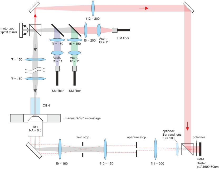
The APVEs are characterized with the home-built imaging system shown in Fig. 8. The setup allows one to focus fiber coupled laser beams of three different wavelengths (Toptica ibeam smart @640 nm, Lasos LGK7786P @543 nm, Thorlabs laser diode PL450B @455 nm) onto the input facet of a APVE, which rests on a manual 3D micro stage. The waists of the laser foci can be controlled by choosing appropriate focal lengths for the lenses 4, 5 and 6. A motorized tip/tilt mirror is imaged onto the APVE input facet using a Keplerian telescope. This allows one to precisely control the laser’s AOI. The output facet is imaged using a microscope objective lens (Olympus UPlanFL, 10x, 0.3 NA), whose exit pupil is imaged onto an iris with tunable aperture. This iris was used to restrict the imaging NA to 0.05 when characterizing the mode sorter. Finally, an image of the end facet is formed at the sensor of a CCD camera (Basler puA1600-60uA). Optionally, a Bertrand lens can be flipped in for imaging the objective’s exit pupil, which is used to calibrate the laser AOIs.
The setup further comprises a Mach-Zehnder interferometer for measuring complex field distributions at the output of the mode sorter APVE using off-axis interferometry.
Interferometry
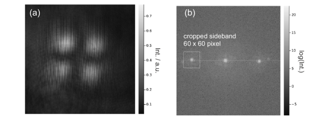
To characterize the quality of the mode sorter, it is required to measure the complex light field at the output facet of the APVE. This is done using off-axis interferometry using a Mach-Zehnder interferometer. The reference wave is tilted, such that the interference fringes have period of about 3 pixels as shown in Fig. 9 (a). The intensity image is Fast Fourier transformed (FFT), followed by cropping a 6060 pixel region around one sideband as shown in Fig. 9 (b). The complex field is then obtained by taking an inverse FFT of the cropped sideband. However, at this stage it will most likely show only a poor overlap with any HG mode. This is because of several factors: Firstly, the field is usually not perfectly centered on the pixel grid and there could be a small geometric rotation in the experimental images. Secondly, the presence of a global phase tilt and defocus is likewise reducing the overlap integral. Finally, the waist of the measured mode could be slightly different compared to the simulation.
To solve these issues, we employed a Nelder Mead optimizer (Julia programming language, toolbox: Optim.jl) to find those seven parameters which maximize the overlap integral between light field obtained at 0∘ AOI and the matching target mode . These parameters are then used to correct all experimentally recorded fields.
Appendix C Additional information on the colour multiplexer
Figure 10 shows output intensities of the colour smiley APVE, taken with the monochromator light source at wavelengths varied from 420 nm to 680 nm in steps of 10 nm. For APVE characterization, the light form the monochromator’s arc lamp was focused into a light guide of 1 mm diameter. About 1 cm from light guide’s output we placed a 100 µm pinhole to further increase the spatial coherence. This pinhole was then imaged with a slight demagnification (telescope with 200 mm and 150 mm lenses) onto the motorized tip/tilt mirror shown in Fig. 8, such that the monochromator light at the input facet of the APVEs took the form of a Gaussian with µm.
Appendix D Additional information on the mode sorter
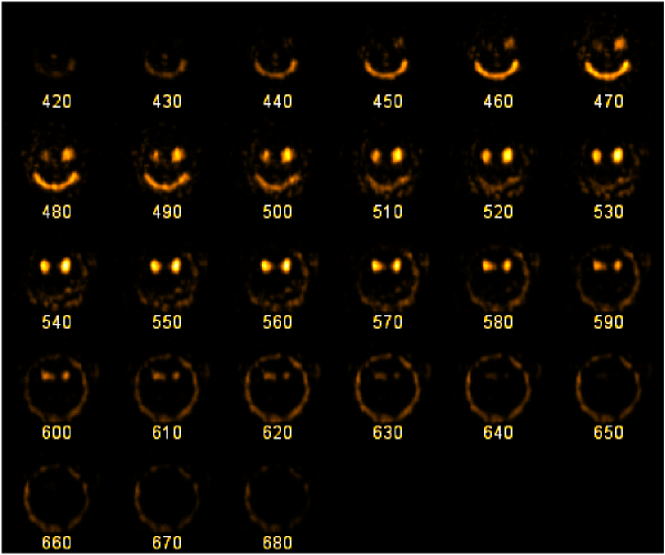
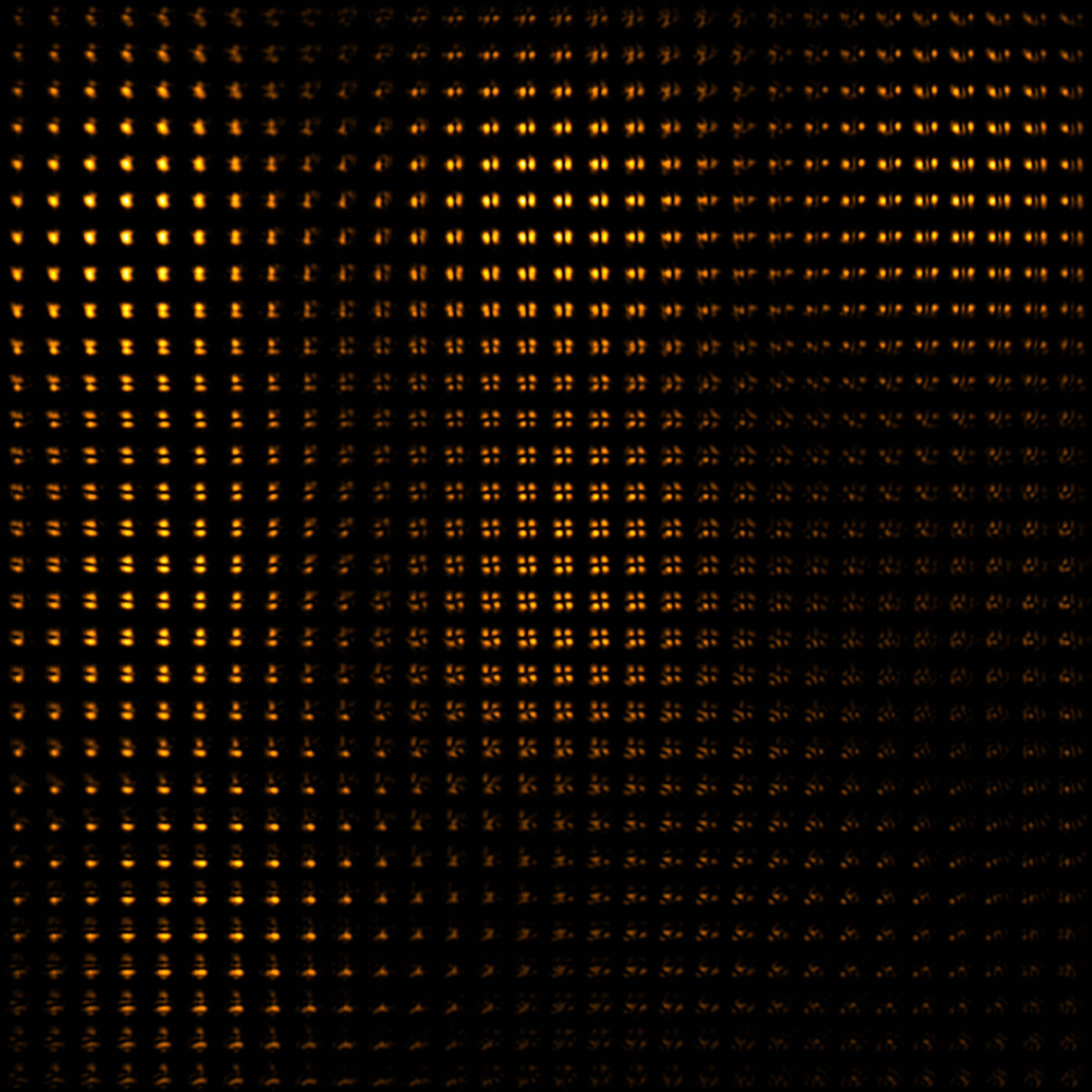
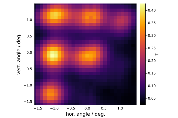
Figure 11 presents a table of 3030 intensity images, which appear at the output facet of the mode sorter when the AOI of the input beam is altered in increments of 0.11 degrees (in air). One can clearly identify six angular regions where the output pattern resembles a particular HG mode. Figure 12 shows the measured transmission of the mode sorter as a function of the laser AOI. One can clearly define six local maxima, whose respective peak values match the numbers in table 5. Finally, Fig. 13 visualizes the measured angular dependence of all six efficiency values as defined by Eq. 3.
Appendix E Manufacturing of APVEs
The APVEs were manufactured using the direct laser writing technique [49]. The beam from an ultrafast laser (Light Conversion, Pharos SP 6W) emitting pulses with 170 fs duration, at a repetition rate of 1 MHz and wavelength 515 nm was expanded and directed toward a phase-only liquid crystal spatial light modulator (SLM) (Hamamatsu X10468). The SLM was imaged in 4f configuration onto the pupil plane of a microscope objective (Zeiss 20 0.5NA). The beam was thus focused into the glass sample (Corning EAGLE 2000) to fabricate the APVE voxels. The sample was mounted on a precision 3D translation stage (Aerotech ABL10100 (x-z), ANT-95V (y)) and moved through the laser focus at a speed of 2 mm/s in the direction, as defined in Figure 1 (a). The PSO function was used to gate the laser according to the design specification and fabricate voxels at the desired position. The laser pulse energy was 37 nJ and the polarisation was linear along the translation direction. We note that this pulse energy is significantly lower than that which would typically be used to write single mode optical waveguides in such a system. As the sample was moved in the direction to build up different layers of the APVE, the phase pattern displayed on the SLM was updated to compensate for depth-induced spherical aberration arising from refraction at the sample surface [50].
Appendix F Design algorithm
In the following, we present an algorithm that allows to design voxel-based APVEs for the conversion of mutually incoherent transverse input modes to target modes , with a one-to-one mapping. In general, any pair of modes has its own wavelength . We consider the design of a finite extent sample in a rectangular coordinate system (), being the direction of propagation. We denote the transverse plane where the input modes are defined, and the destination plane where the target modes are defined. The bulk refractive index of the sample at wavelength is denoted . In terms of fabrication capabilities, we assume that we have access to a diversity of transverse voxel distributions that we are able to write in the glass sample at any 3D location, and that the length of any voxel (i.e., the dimension) can be freely chosen. One example of a voxel cross section is given in Figure 1 (b), but many more are possible by varying the writing parameters such as the pulse energy or the aberration compensation term. Let us note the number of different transverse voxel distributions which we consider to use for the inverse design. These transverse distributions are relative refractive index changes compared to the bulk refractive index, and are possibly wavelength dependent. By convention, we also define to refer to a null refractive index modification. In order to make the inverse design much simpler, the sample volume is virtually split into sub-volumes , , , , acting as placeholders for the elementary voxel distributions . These sub-volumes extensions in 3 dimensions are denoted , and . Thus, the possible lengths of the waveguides used for the design can only be integer multiples of the elementary length . In our designs, this elementary length is typically . For the simulation to be numerically accurate, the sampling resolution in 3 dimensions , and must be much better, typically and .
Forward model
The propagation of the input modes from the plane to the plane relies on the split-step Fourier beam propagation method (BPM), with spatial resolutions , and . The input modes cross the sub-volumes layer by layer, for varying from 1 to . Each sub-volume may contain (or not) one of the possible transverse distributions , depending on the choice that was made in a previous iteration by the selection algorithm that we present next. During this forward propagation, the transverse distributions are saved before crossing each sub-volume , and we note them for future reference. We also note the common transverse planes where these distributions are saved.
According to the BPM, for a given input mode , crossing each layer of thickness is modeled as a small propagation of length through an homogeneous medium of refractive index , followed by the multiplication of a local phase depending on the activated region:
| (4) |
Error metric
Our inverse design relies on a multi-objective minimization based on the squared distance between the input and target modes:
| (5) |
We can expand the squared modulus as , which allows to turn the minimization problem (5) into the following maximization problem in the case of a lossless design ( of and is conserved):
| (6) |
The expression (6) consists only of overlap integrals that are conserved during propagation (or backpropagation) through a lossless optical system, thus allowing for an iterative propagation algorithm (IPA) [51], where the same criterion is iteratively maximized in each plane (in a reverse fashion).
Voxel distribution selection algorithm
We assume that we know the transverse distributions corresponding to the local distributions of the target modes in the plane just after the sub-volumes , and the transverse distributions of the input modes stored just before the same sub-volumes. The selection of the refractive index distribution relies on the maximization of the local multi-objective criterion
| (7) |
where denotes the local input modes distribution that have been propagated from plane , where they were stored during the forward pass, to plane through a local refractive index distribution . In order to find maximizing , all the distributions need to be tried for each sub-volume ( fixed).
Once the distributions have been selected for a given , the target modes are backpropagated to the plane , and the same procedure is repeated iteratively until the selection of the .
Iterative propagation algorithm
We summarize the different steps of the optimization procedure below:
-
1.
Propagate the input modes from their definition plane to the destination plane using BPM, taking into account the current waveguide selection in each sub-volume (). At the beginning of the first iteration, all contain a null refractive index distribution (). During propagation, store the local field distributions at planes .
-
2.
Compute the final overlap criterion (6) for monitoring the convergence of the algorithm. If the convergence is satisfactory or stagnant, then exit the optimization procedure and consider the current waveguide selection as the optimal design.
-
3.
Iteratively backpropagate the target modes from plane to plane , while proceeding to a new voxel selection in each sub-volume according to criterion (7). For a given , this criterion leads to the best voxel selection in each sub-volume, after which the modes in plane can be backpropagated to plane , and this iteratively until .
-
4.
Repeat the procedure from step 1.