Spin-active single photon emitters in hexagonal boron nitride from carbon-based defects
Abstract
Most single photon emitters in hexagonal boron nitride have been identified as carbon substitutional defects, forming donor-acceptor systems. Unlike the most studied bulk emitters (i.e. color centers in diamond), these defects have no net spin, or have a single unpaired spin. By means of density functional calculations, we show that two non-adjacent carbon substitutional defects of the same type (i.e. CB-CB, and CN-CN), can have a triplet groundstate. In particular, one of such defects has a zero phonon line energy of 2.5 eV, and its triplet state is nearly 0.5 eV more stable than its singlet. The mechanism behind the destabilization of the singlet state is related to a larger electrostatic repulsion of a symmetric wave function in a charged lattice.
I Introduction
The study and identification of the atomic defects associated with single photon emitters (SPEs) in hexagonal boron nitride (h-BN) is an active topic.[1, 2, 3, 4] Excluding atomically engineered defects,[5, 6] experiments suggest C-based defects as SPEs.[7] So far, several substitutional C defects have been proposed. Those include monomers, different dimers (i.e. including non-adjacent atoms), trimers, arrangements of two close defects, and bigger substitutional clusters.[8, 9, 10, 11, 12, 13, 14, 15] All these defects follow a similar logic, when a C atom replaces a B(N) atom, i.e. a CB (CN) defect, it behaves as a donor(acceptor). Larger defects, with an even number of defect atoms, are built to have as many donors as acceptors, and the occupied and empty states will have a sizable band gap (we will elaborate on this at the beginning of Sec. III). The case with an odd number of C atoms is similar, but with single uncompensated donor or acceptor, leading to a single extra energy level within the fundamental band gap. From this construction there exist only two possible spin configurations: (i) if the number of C atoms of the defect is even, the SPE has no net spin; (ii) if the number is odd, the SPE is paramagnetic with spin .[8, 9]
To the best of our knowledge, there are only a few types of C-based proposals of high-spin SPEs, with . One combines a substitutional and an out-of-plane interstitial defect.[16] These defects offer an excellent example, beyond of the donor-acceptor logic, of a high-spin groundstate. The aforementioned defects have a set of zero phonon lines (ZPL) consistent with experimental results.[16] Nevertheless, interstitials defects have a large formation energy and small migration barriers,[17] and the natural occurrence of these defects should be rather scarce, due to their high formation energy. The second is a combination of a vacancy with a substitutional C atom.[18] Again, the formation energy of these defects prevent them from being found in large concentrations.[17] The formation energy, of a defect strongly depends on the chemical potential and Fermi energy, for single substitutional defects they are in the range eV. Excluding very specific combinations of Fermi energy and chemical potential, the of vacancies or interstitials is at least 2 eV higher than in substitutions.[17, 16, 19]
The last proposal of SPEs with , introduced by Maciaszek et al.[17], is formed by four star-like substitutional C atoms: C and C, they have a ZPL energy eV. These defects are an excellent example of pure substitutional C defects beyond from the standard donor-acceptor logic. However, these clusters only could be found in particular conditions (N-poor or N-rich), and with a rather low concentration (between two to three orders smaller than dimer or trimer defects).[17]
Experimentally, optically-detected magnetic resonance (ODMR) has been employed to detect the spin from SPEs. Most of the measurements are associated with the V defect.[20, 21, 22] However, there is evidence of other spinful defects,[23, 7, 24, 25] with a photoluminescence spectra consistent with pure substitutional C defects. Particularly, a recent study[26] has shown that a spin or is required to explain their ODMR measurements.
In this article, we show that two substitutional C defects of the same type (i.e. CNCN or CBCB) can have a triplet groundstate, which in most cases is just a few meV lower in energy than the singlet. However, there is a specific defect where the triplet state is nearly 0.5 eV more stable. We start by explaining our calculation methods in Sec. II. Then we show our results (Sec. III), starting with the simplest CB and CN defects and continuing with the dimer defects. Finally, in Sec. IV, we provide an explanation of our findings.
II Computational Methods
Our central goal is to show that a triplet groundstate can be achieved with C-substitutional defects, even though it may seem counterintuitive at first glance. Then we will focus on the luminescent properties of the most interesting defect found. Our methodology reflects these goals, providing details about the accuracy of our calculations and measures to avoid possible methodological errors. Then, we explain the methodology used to calculate some properties: formation energy, ZPL energy, Huang-Rhys and Debye-Waller factors.
II.1 Calculation parameters and approximations
The calculations were performed with density functional theory (DFT), mostly by using the VASP package[27, 28, 29, 30], but we also used the Gaussian code[31] in a few test calculations, as explained later in the text.
Regarding the settings of the VASP calculations (plane waves), the Perdew–Burke-Ernzerhof (PBE) and the Heyd–Scuseria–Ernzerhof (HSE) functionals were used.[32, 33, 34] The PBE functional gives a correct description of forces and geometries, however it has some shortcomings related to energies: (i) it underestimates the fundamental band gap of h-BN,[35] (ii) it underestimates the ZPL of C-based SPEs,[8] and (iii) it has problems representing the right distribution of localized states such as defect states. Conversely, the hybrid HSE functional gives quantitatively meaningful results, at a much higher computational cost.[36] One of the most important advantages of the HSE functional is the inclusion of Hartree-Fock exchange in the short-range part of the Coulomb interaction, which is important for accurately describing the difference in energy between states of different multiplicity. The HSE functional has a free parameter, defining the limit between short- and long-range of the Coulomb interaction. We used the popular so-called HSE06 version of the functional, i.e. the screening parameter is bohr-1 and the relative amount of Hartree-Fock exchange was 1/4.[34] Nevertheless, due to the decreased screening of 2D materials -such as h-BN- in some studies the value of the free parameter is changed to adjust the material’s band gap.[9] We do not expect a qualitative change by changing the form of the HSE functional (see Ref. [37] for a longer discussion on this topic).
Regarding the other parameters and settings of the calculations (VASP code), projector augmented-wave pseudopotentials were used.[38] A kinetic energy cutoff of 400 eV was employed, we tested a larger cutoff (650 eV) and it did not change the results significantly (see the Appendix). A single k-point () was used in the supercell calculations. PyProcar was employed for the analysis of the results,[39] and VESTA for the visualization.[40] The geometries were relaxed with PBE in both the ground and excited states. The relaxation with HSE06 of a specific defect, led to very similar results,[9] see Table 5 in the Appendix. The lattice parameter was set to 2.49 Å, the equilibrium value obtained with HSE06.
An especially tricky point could be the usage of periodic boundary conditions (PBC), at least for the systems with a small difference between the singlet and triplet states. All the PBC calculations shown here use a supercell and the HSE06 functional. These calculations were tested at the PBE level with supercells ranging from to . The differences due to the supercell size were minimal. Convergence tests of the supercell size with HSE06 are given in the Appendix. It is worth remarking that the HSE06 functional should be even less dependent on the supercell size, since it provides a much better localization of the defect’s states.
To discard artifacts from the PBC, we used cluster models as explained in more detail in the Appendix. The shape of the clusters is critical for CNCN clusters. Most cluster calculations were performed with VASP using the previous parameters, only the kinetic energy cutoff was increased to 500 eV, to better represent the finite size of the clusters. A few comparison calculations were performed with the Gaussian software, obtaining a good agreement between both codes. These calculations were done with the Gaussian 09.[31] For these calculations two double-Z basis set were used: 6-31+G(d) and cc-pVDZ.
II.2 Calculation of physical properties
The formation energy of a defect in a charge state is:
| (1) |
where is the total energy of a supercell hosting the defect in the desired charge state, is the energy of a pristine h-BN supercell, is the chemical potential of element . is the change in the number of atoms of element , with respect to the pristine supercell. The Fermi energy is set to zero at the valence band maximum. are corrections of large importance in charged defects.[41, 42] Since the defects we studied are neutral, , there is no need for an electrostatic correction.
The chemical potential represents a reservoir for the exchange of atoms. We took as reference for , , and , the energy per atom of bulk B, the N2 molecule, and graphite, respectively. To simulate the limits of N-rich and N-poor conditions we followed the approach of Ref. [19].
The excited states were studied by means of the SCF method.[43] The singlet groundstate is spin degenerate and its excitation is from the last occupied level to the first empty. For the triplet groundstate, the excitation with lowest energy also is from the last occupied level to the first empty, but the spin channel depends on the system: in CBCB the transition takes place on the majority spin, while in CNCN the excitation takes place on the minority spin.
The Huang-Rhys factor measures the quantity of phonons participating in the ZPL transition. To obtain it, generalized coordinates are needed.[44]
| (2) |
where the indexes , and denote atoms, Cartesian coordinates and vibrational modes, respectively. and are the positions in the excited and ground state, respectively. is the mass of atom , and is the unitary vector of the -th vibrational mode. Also, in this step we assumed that the vibrational modes for the ground and excited states are identical. In short, the above equation is a decomposition of the atomic rearrangement due to an optical excitation in the basis of the phonons.
The partial Huang-Rhys factor, , quantifies the number of phonons of a given vibrational mode in the transition:
| (3) |
where represents the frequency of the phonon. Finally, the Huang-Rhys factor is obtained by adding all these partial factors, . On the other hand, the Debye-Waller factor measures the weight of the ZPL peak, , with respect to the total photoluminescence spectrum. Since there is no emission of phonons at the ZPL, .[44]
III Results
III.1 The CB and CN defects
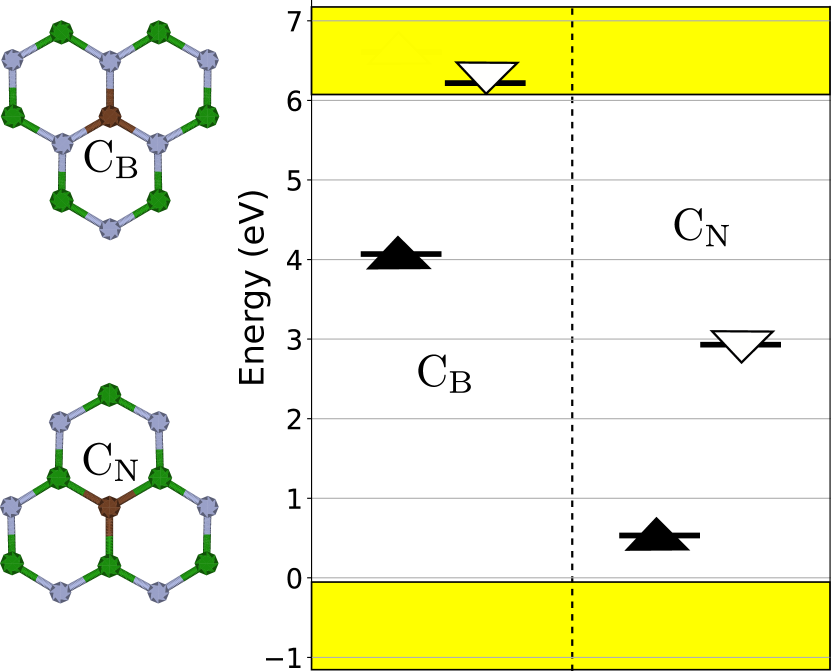
The simplest substitutional C defects are the replacement of a B or N atom by a carbon, they are denoted CB and CN, respectively, see Fig. 1. When neutral, these defects are candidates for SPEs within the visible range.[8, 9] In what follows we will focus only in the neutral cases. Both defects have groundstates within the fundamental band gap of h-BN. Each defect has a paramagnetic groundstate, , and meanwhile CB acts as a donor, with its last occupied level close to the conduction band, CN acts like an acceptor with its first empty band near the middle of the band gap. If a CB and a CN are close enough, they form a dimer-like state, CC, which is non-magnetic. It shows luminescence with a ZPL that varies with the separation between the CN and CB defects.[9]
III.2 The CBCB and CNCN dimers
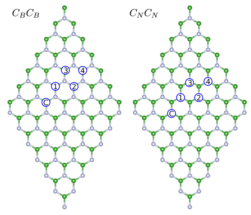
The simplest way to avoid a donor-acceptor pair with a singlet groundstate is to consider two close defects of the same type, CB or CN. Up to a few lattice sites, their localized states overlap, and they can be considered as a single defect. See Fig. 2 for the geometry and labeling of the systems under study.
The formation energy, , of the defects presented here is shown in Table 1 for two extreme conditions denoted as N-rich and N-poor, described in Sec. II. As expected, these values are similar to other C-based defects in h-BN, and their abundance should be determined by the actual environment.[17]
| Configuration | Hf (eV) | |
|---|---|---|
| N-poor | N-rich | |
| CNCN-2 | 3.82 | 9.02 |
| CNCN-3 | 3.82 | 9.02 |
| CNCN-4 | 3.83 | 9.03 |
| CBCB-2 | 8.47 | 3.27 |
| CBCB-3 | 8.49 | 3.29 |
| CBCB-4 | 8.47 | 3.27 |
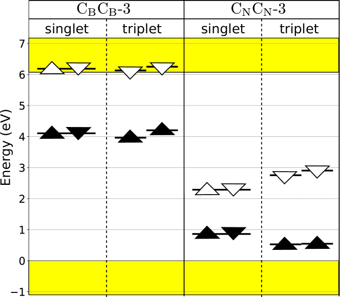
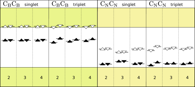
When both defect atoms are not too close (i.e. beyond nearest neighbors), their levels can be inferred up to some extent from the monomers, see Fig. 1 as reference, with two possible arrangements, the singlet and the triplet. The actual energy levels for a specific distance are shown in Fig. 3. The visual inspection of the CBCB-3 dimer shows no appreciable difference between the single and triplet arrangements. However, CNCN-3 shows a much larger separation between the occupied and empty defect levels in the triplet, lowering the total energy. The different values of the defect levels as a function of the distance is shown in Fig. 4. The defects of the CBCB family do not show any appreciable difference in the singlet states as a function of the distance. However, in the triplet there is an appreciable distance-dependent interaction for the same spin value. Just from inspecting the energy levels the groundstate is not evident, e.g. the singlet and triplet have a comparable energy. The CNCN defects show a similar pattern with the exception of CNCN-3, which was already discussed and it will be explained in more detail in Sec. IV.
| Label | distance (Å) | (meV) |
| CB-CB-2 | 4.32 (4.32) | -27 |
| CB-CB-3 | 4.98 (4.98) | 32 |
| CB-CB-4 | 6.61 (6.61) | 20 |
| CN-CN-2 | 4.33 (4.35) | -44 |
| CN-CN-3 | 5.02 (5.03) | 482 |
| CN-CN-4 | 6.61 (6.62) | 19 |
The actual differences in total energy of all the systems studied are in Table 2. In general, for closer defects (CXCX-2) the singlet state is slightly more stable. For longer distances (CXCX-4) the opposite is true. In the remaining case, CXCX-3, for B defects, shows an intermediate behavior, with both configurations almost degenerate in energy. However, in CNCN-3 the triplet is nearly 0.5 eV more stable than the singlet. Although this last result may seem strange at first glance, in the next section we will show that a lower energy for the triplet is to be expected. Additionally, an extensive set of convergence tests, including cluster models, is in the Appendix.
The defects CXCX-3 share have in common a triplet groundstate. They can have an optical transition from the valence band to the unoccupied defect states. The zero phonon line (ZPL) of CNCN-3 has energy eV, if the lowest energy level is involved in the transition. Its Huang-Rhys and Debye-Waller factors are and , respectively. In contrast, the defect CBCB-3, has a ZPL energy eV, a much smaller electron-phonon, with and .
For the sake of comparison, experiments in h-BN, have found a myriad of SPEs, with wavelength covering the visible spectrum,[45] likely most of them are C-substitutional defects forming a donor-acceptor pair. Experimental values of the Huang-Rhys factor[10] are (). Also it is insightful to compare CXCX-3 defects with the NV- and SiV0 defects found in bulk diamond, all of them with a triplet groundstate. The ZPL energy of the NV- center is eV, and a very prominent phonon side-band, ().[46] The SiV0 center has eV, and a remarkably small electron-phonon coupling, ().[47] In this respect, h-BN C-based defects have some clear advantages and drawbacks compared with their bulk diamond counterparts. First, a 2D material hosting the SPEs allows a much easier integration into devices, even more, there is unprecedented possibility of controlling the SPE by forming a van der Waals heterostructure.[48] Second, C-based SPEs in h-BN offer a ‘ultrabright’ stable luminescent signal, overcoming the signal of the NV- and SiV centers.[49] We expect a similar behavior of the SPEs presented here. Third, the SPEs studied here have a small electron-phonon coupling, favoring long coherence times. However, the SiV center has an even smaller electron-phonon coupling, useful for quantum technologies. Fourth, there is a widespread problem to generate specific C-based SPEs in h-BN. We are aware of two reports of monochromatic SPEs in h-BN, blue[3] and yellow,[50] neither of them seems to be spin-active.
The energy difference of most CXCX defects is smaller than room temperature ( meV), but larger than the critical temperature of liquid nitrogen (7 meV), which is easy to reach in experiments and make our predictions susceptible to experimental test. The triplet state in the defect CNCN-3 should remain stable even near the dissociation temperature of h-BN ( K).
IV Discussion
A simple model for the CXCX defects is a two-electron molecule in an effective medium, similar to the H2 molecule, but with extra terms in the Hamiltonian due to the h-BN lattice. The Hamiltonian is:
| (4) |
where is the standard Hamiltonian of a H2-like system,
| (5) |
with the sub-indexes {1,2} labelling both electrons, and the substitutional ions are denoted as {A,B}. The distances are . The contribution of the lattice to the CXCX Hamiltonian can be modeled as an electrostatic-only contribution:
| (6) |
Here, the effective charge of each site, which is negative (positive) for the N (B) atoms, see Fig. 5.
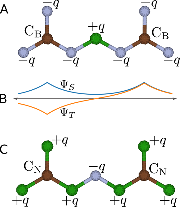
The solutions to Eq. 5 can be symmetric in the orbitals or in the spin, forming a singlet or a triplet, respectively. Without the lattice potential (), the relative energy of both states is given by exchange and Coulomb integrals. The singlet state always has a lower energy, as it is well established [51].
Considering exponentially decaying states for the defect wave functions, the energy associated to will be similar for both the singlet and triplet for most lattice sites. This is because the localized wave function is relevant only for a few nearest neighbors, and the effects of having a (anti-) symmetric wave function are relevant only where the contribution of both states is non-negligible. However, there is a position of the lattice which is particularly relevant, at least for the CXCX-3 defects. See Fig. 5, the atom at the midpoint between both C atoms is located in a region where the amplitude of the wavefunctions of the defect is not negligible. This atom is only 2.5 Å apart from the C positions. Also, it can have a positive or negative net charge, which implies that this site is attractive for electrons in the case of the CBCB-3 defect and repulsive in the case of CNCN-3. If we label this atoms as , the energy associated to this site is
| (7) |
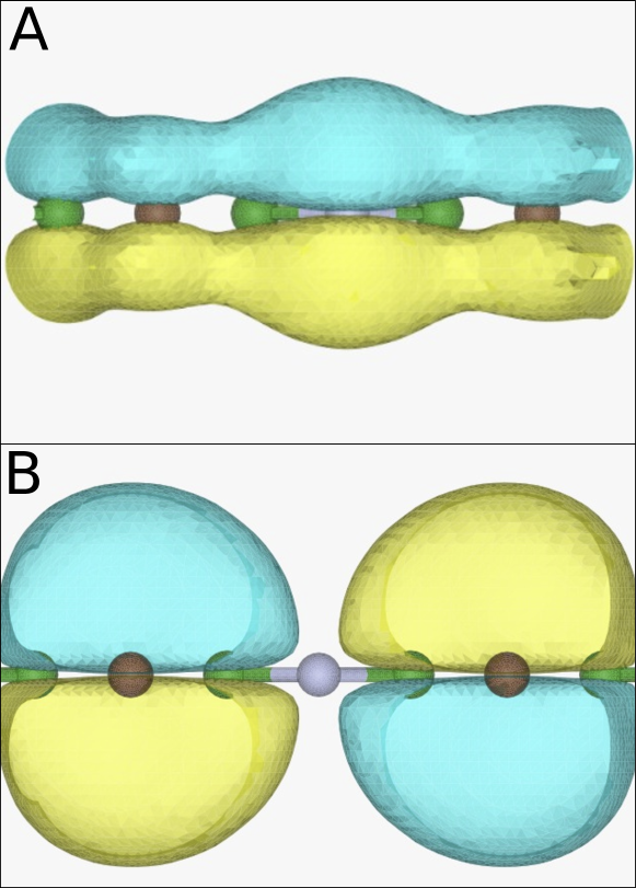
where for a singlet or triplet state. For CBCB-3, since the charge is positive, a larger amplitude of in this atom is favored. This is achieved in the nodeless singlet state, and is such that . Contrary , for CNCN-3, the potential due to the site is repulsive for electrons, and the anti-symmetry of the triplet lowers the total energy: . Therefore, favors a triplet (singlet) for CNCN-3 (CBCB-3). The difference between the singlet and triplet wave function for CNCN-3 is shown in Fig. 6, note the absence or presence of a central node. It is worth mentioning that with this simple analysis we only intend to provide an ex post explanation of our results. The simplicity of the model does not allow us to predict which will be the most stable state, the singlet or the triplet.
V Conclusions
By means of DFT calculations we found that two substitutional CN or CB defects of the same type, have a triplet () groundstate when both C atoms are sufficiently separated. In particular, when two CN atoms are separated by two lattice parameters ( Å, denoted CNCN-3 in the article) the triplet state is lower in energy by eV, compared with the singlet state. The ZPL associated with this defect is eV. In the remaining cases the energy difference between the triplet and singlet states is smaller than eV.
The defect CNCN-3 could explain the measured defects in h-BN with .[23, 7, 25, 26] Since no vacancy is involved, they should have a large abundance[17]. Also, as pure substitutional C defects, they should exhibit the typical phonon sideband (PSB) with lateral maximum shift meV from the ZPL.[8].
On the other hand, the remaining non-adjacent CNCN and CBCB defects have a rather small energy difference between both the triplet and singlet state. Therefore, it could be possible to induce a switch between both states by means of an external field, or in a van der Waals heterostructure.
VI Competing Interests
The Authors declare no Competing Financial or Non-Financial Interests
VII Data Availability
All input files are available from the corresponding author upon reasonable request.
VIII Author Contributions
F.P., C.C., N.V and F.M. run all the calculations. F.M. conceived the idea. F.M., J.R.M., and C.C. explained the stability of the triplet state. All authors discussed the results and contributed to the writing of the manuscript.
Acknowledgements.
This work was partially supported by Fondecyt Grants No. 1191353, 1220715, 1220366, and 1221512 by the Center for the Development of Nanoscience and Nanotechnology CEDENNA AFB180001, and from Conicyt PIA/Anillo ACT192023. This research was partially supported by the supercomputing infrastructure of the NLHPC (ECM-02).Appendix A Convergence and boundary conditions
The results from Table 2, shows a drastic difference between one particular defect and the others. It is valid to ask whether these results are an artifact from the calculations or not. In this aspect we will show that for a large set of parameters the results do hold.
The first aspect to test is the role of the supercell size. We focus on the trends of the CN-CN defects with the HSE06 functional, since these defects show the abrupt changes. Table 3 shows the same behavior regardless of the size of the supercell. For the most separated defects, CN-CN-4, the supercell influences the results in the range of a few meV.
| Label | Supercell | (meV) |
| CN-CN-2 | -44 | |
| CN-CN-2 | -44 | |
| CN-CN-2 | -44 | |
| CN-CN-3 | 486 | |
| CN-CN-3 | 482 | |
| CN-CN-3 | 482 | |
| CN-CN-4 | 27 | |
| CN-CN-4 | 15 | |
| CN-CN-4 | 19 |
The completeness of the plane-wave basis is given by the kinetic energy cutoff, and in defect calculations it is critical to resolve localized states. We extensively tested the cutoff with the PBE functional (not shown here). Obtaining that a cutoff of 400 eV is good enough to have an accuracy of a few meVs. However, our results suggest that PBE is unable to correctly capture the localization of the defect’s electron density. To check the accuracy of our results with a cutoff of 400 eV, we tested a cutoff of 650 eV for two defects with the most interesting/complex interplay between localization and electronic occupations. While at first glance it may be surprising that a cutoff of 400 eV is enough to describe localized defect states, this is the cutoff recommended in the pseudopotential to describe localized states, such as the h-BN bonds.
| Label | cutoff (eV) | (meV) |
|---|---|---|
| CN-CN-3 | 400 | 482 |
| CN-CN-3 | 650 | 484 |
| CB-CB-3 | 400 | 32 |
| CB-CB-3 | 650 | 31 |
Another test is the effect of the atomic relaxation with HSE06, compared with the relaxation with PBE followed by a static calculation with HSE06. Again, we only tested the CN-CN defects. Table 5 shows a minor effect of the functional regarding the relative stability of the singlet/triplet states. This is because (i) PBE provides decent forces and positions, and (ii) the error in positions due to PBE is likely to be consistent (e.g. longer C-N bonds) and cancelled when measuring relative energies.
| Label | relaxation | (meV) |
|---|---|---|
| CN-CN-2 | HSE06 | -44 |
| CN-CN-2 | PBE | -44 |
| CN-CN-3 | HSE06 | 474 |
| CN-CN-3 | PBE | 482 |
| CN-CN-4 | HSE06 | 16 |
| CN-CN-4 | PBE | 15 |
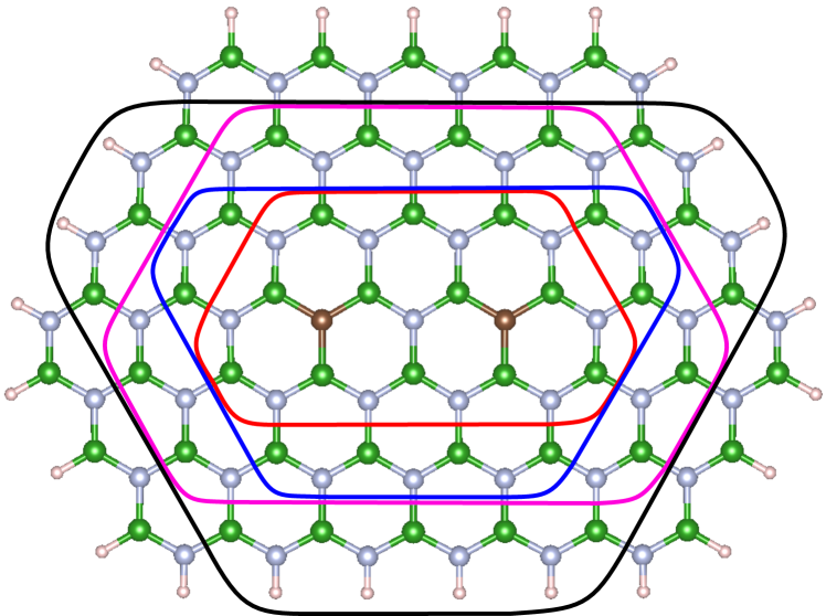
The last test we made, is to use a cluster model to rule out artifacts from the PBC. The clusters are shown in Fig. 7. All the clusters are passivated with H atoms, and were created with pyPoscar[52]. The results are given in Table 6, and show a good agreement with supercell calculations. A strange trend is evident from the Table 6 with a minimum energy at B28N27C2, and it increases for larger and smaller clusters. We interpret such behavior in terms of the localization of the defect wave functions, for smaller clusters it is spuriously localized, resulting in an increased interaction for both spin configurations. As the size of the system increases, the cluster boundaries become less relevant. However, it does not happen at the same rate. The triplet state is less localized, needing a larger cluster to avoid artifacts due to the finite boundaries. That extra interaction results in lower total energy of the triplet, in concordance with Table 6. Since we used a larger cutoff energy and supercell size in these calculations, a perfect agreement with the results of periodic systems is unlikely.
References
- White et al. [2021] S. White, C. Stewart, A. S. Solntsev, C. Li, M. Toth, M. Kianinia, and I. Aharonovich, Phonon dephasing and spectral diffusion of quantum emitters in hexagonal boron nitride, Optica 8, 1153 (2021).
- Román et al. [2021] R. J. P. Román, F. J. R. C. Costa, A. Zobelli, C. Elias, P. Valvin, G. Cassabois, B. Gil, A. Summerfield, T. S. Cheng, C. J. Mellor, P. H. Beton, S. V. Novikov, and L. F. Zagonel, Band gap measurements of monolayer h-BN and insights into carbon-related point defects, 2D Materials 8, 044001 (2021).
- Gale et al. [2022] A. Gale, C. Li, Y. Chen, K. Watanabe, T. Taniguchi, I. Aharonovich, and M. Toth, Site-specific fabrication of blue quantum emitters in hexagonal boron nitride, ACS Photonics 9, 2170 (2022).
- Kianinia et al. [2022] M. Kianinia, Z.-Q. Xu, M. Toth, and I. Aharonovich, Quantum emitters in 2d materials: Emitter engineering, photophysics, and integration in photonic nanostructures, Applied Physics Reviews 9, 011306 (2022).
- Kianinia et al. [2020] M. Kianinia, S. White, J. E. Fröch, C. Bradac, and I. Aharonovich, Generation of spin defects in hexagonal boron nitride, ACS Photonics 7, 2147 (2020).
- Gao et al. [2021] X. Gao, S. Pandey, M. Kianinia, J. Ahn, P. Ju, I. Aharonovich, N. Shivaram, and T. Li, Femtosecond laser writing of spin defects in hexagonal boron nitride, ACS Photonics 8, 994 (2021).
- Mendelson et al. [2021] N. Mendelson, D. Chugh, J. R. Reimers, T. S. Cheng, A. Gottscholl, H. Long, C. J. Mellor, A. Zettl, V. Dyakonov, P. H. Beton, S. V. Novikov, C. Jagadish, H. H. Tan, M. J. Ford, M. Toth, C. Bradac, and I. Aharonovich, Identifying carbon as the source of visible single-photon emission from hexagonal boron nitride, Nature materials 20, 321 (2021).
- Jara et al. [2021] C. Jara, T. Rauch, S. Botti, M. A. L. Marques, A. Norambuena, R. Coto, J. E. Castellanos-Águila, J. R. Maze, and F. Munoz, First-principles identification of single photon emitters based on carbon clusters in hexagonal boron nitride, J. P. Chem. A 125, 1325 (2021).
- Auburger and Gali [2021] P. Auburger and A. Gali, Towards ab initio identification of paramagnetic substitutional carbon defects in hexagonal boron nitride acting as quantum bits, Phys. Rev. B 104, 075410 (2021).
- Li et al. [2022a] K. Li, T. J. Smart, and Y. Ping, Carbon trimer as a 2 ev single-photon emitter candidate in hexagonal boron nitride: A first-principles study, Phys. Rev. Materials 6, L042201 (2022a).
- Winter et al. [2021] M. Winter, M. H. E. Bousquet, D. Jacquemin, I. Duchemin, and X. Blase, Photoluminescent properties of the carbon-dimer defect in hexagonal boron-nitride: A many-body finite-size cluster approach, Phys. Rev. Materials 5, 095201 (2021).
- Golami et al. [2022] O. Golami, K. Sharman, R. Ghobadi, S. C. Wein, H. Zadeh-Haghighi, C. Gomes da Rocha, D. R. Salahub, and C. Simon, and group theoretical study of properties of a carbon trimer defect in hexagonal boron nitride, Phys. Rev. B 105, 184101 (2022).
- Huang et al. [2021] P. Huang, M. Grzeszczyk, K. Vaklinova, K. Watanabe, T. Taniguchi, K. Novoselov, and M. Koperski, Carbon and vacancy centers in hexagonal boron nitride, arXiv preprint arXiv:2112.14906 (2021).
- Li et al. [2022b] S. Li, A. Pershin, G. Thiering, P. Udvarhelyi, and A. Gali, Ultraviolet quantum emitters in hexagonal boron nitride from carbon clusters, The Journal of Physical Chemistry Letters 13, 3150 (2022b).
- Amblard et al. [2022] D. Amblard, G. D’Avino, I. Duchemin, and X. Blase, Universal polarisation energies for defects in monolayer, surface and bulk hexagonal boron nitride: A finite-size fragments gw approach, arXiv preprint arXiv:2204.11671 (2022).
- Bhang et al. [2021] J. Bhang, H. Ma, D. Yim, G. Galli, and H. Seo, First-principles predictions of out-of-plane group iv and v dimers as high-symmetry, high-spin defects in hexagonal boron nitride, ACS Applied Materials & Interfaces 13, 45768 (2021).
- Maciaszek et al. [2022] M. Maciaszek, L. Razinkovas, and A. Alkauskas, Thermodynamics of carbon point defects in hexagonal boron nitride, Phys. Rev. Materials 6, 014005 (2022).
- Cheng et al. [2017] G. Cheng, Y. Zhang, L. Yan, H. Huang, Q. Huang, Y. Song, Y. Chen, and Z. Tang, A paramagnetic neutral cbvn center in hexagonal boron nitride monolayer for spin qubit application, Computational Materials Science 129, 247 (2017).
- Weston et al. [2018] L. Weston, D. Wickramaratne, M. Mackoit, A. Alkauskas, and C. G. Van de Walle, Native point defects and impurities in hexagonal boron nitride, Phys. Rev. B 97, 214104 (2018).
- Mathur et al. [2022] N. Mathur, A. Mukherjee, X. Gao, J. Luo, B. A. McCullian, T. Li, A. N. Vamivakas, and G. D. Fuchs, Excited-state spin-resonance spectroscopy of v defect centers in hexagonal boron nitride, Nature Communications 13 (2022).
- Baber et al. [2022] S. Baber, R. N. E. Malein, P. Khatri, P. S. Keatley, S. Guo, F. Withers, A. J. Ramsay, and I. J. Luxmoore, Excited state spectroscopy of boron vacancy defects in hexagonal boron nitride using time-resolved optically detected magnetic resonance, Nano Letters 22, 461 (2022).
- Yu et al. [2022] P. Yu, H. Sun, M. Wang, T. Zhang, X. Ye, J. Zhou, H. Liu, C.-J. Wang, F. Shi, Y. Wang, and J. Du, Excited-state spectroscopy of spin defects in hexagonal boron nitride, Nano Letters 22, 3545 (2022).
- Guo et al. [2023] N.-J. Guo, S. Li, W. Liu, Y.-Z. Yang, X.-D. Zeng, S. Yu, Y. Meng, Z.-P. Li, Z.-A. Wang, L.-K. Xie, R.-C. Ge, J.-F. Wang, Q. Li, J.-S. X. Xu, Y.-T. Wang, J.-S. Tang, A. Gali, and G.-C. Li, Chuan-Feng anf Gup, Coherent control of an ultrabright single spin in hexagonal boron nitride at room temperature, Nature Communications 14, 2893 (2023).
- Chejanovsky et al. [2021] N. Chejanovsky, A. Mukherjee, J. Geng, Y.-C. Chen, Y. Kim, A. Denisenko, A. Finkler, T. Taniguchi, K. Watanabe, D. B. R. Dasari, P. Auburger, A. Gali, J. H. Smet, and J. Wrachtrup, Single-spin resonance in a van der waals embedded paramagnetic defect, Nature materials 20, 1079 (2021).
- Liu et al. [2022] W. Liu, N.-J. Guo, S. Yu, Y. Meng, Z.-P. Li, Y.-Z. Yang, Z.-A. Wang, X.-D. Zeng, L.-K. Xie, Q. Li, J.-F. Wang, J.-S. Xu, Y.-T. Wang, J.-S. Tang, C.-F. Li, and G.-C. Guo, Spin-active defects in hexagonal boron nitride, Materials for Quantum Technology 2, 032002 (2022).
- Stern et al. [2022] H. L. Stern, Q. Gu, J. Jarman, S. Eizagirre Barker, N. Mendelson, D. Chugh, S. Schott, H. H. Tan, H. Sirringhaus, I. Aharonovich, and M. Atatüre, Room-temperature optically detected magnetic resonance of single defects in hexagonal boron nitride, Nature communications 13, 1 (2022).
- Kresse and Hafner [1993] G. Kresse and J. Hafner, Ab initio molecular dynamics for liquid metals, Phys. Rev. B 47, 558(R) (1993).
- Kresse and Hafner [1994] G. Kresse and J. Hafner, Ab initio molecular-dynamics simulation of the liquid-metal–amorphous-semiconductor transition in germanium, Phys. Rev. B 49, 14251 (1994).
- Kresse and Furthmüller [1996] G. Kresse and J. Furthmüller, Efficiency of ab-initio total energy calculations for metals and semiconductors using a plane-wave basis set, Comput. Mater. Sci. 6, 15 (1996).
- Kresse and Furthmüller [1996] G. Kresse and J. Furthmüller, Efficient iterative schemes for ab initio total-energy calculations using a plane-wave basis set, Phys. Rev. B 54, 11169 (1996).
- Frisch et al. [2009] M. J. Frisch, G. W. Trucks, H. B. Schlegel, G. E. Scuseria, M. A. Robb, J. R. Cheeseman, G. Scalmani, V. Barone, B. Mennucci, G. A. Petersson, H. Nakatsuji, M. Caricato, X. Li, H. P. Hratchian, A. F. Izmaylov, J. Bloino, G. Zheng, J. L. Sonnenberg, M. Hada, M. Ehara, K. Toyota, R. Fukuda, J. Hasegawa, M. Ishida, T. Nakajima, Y. Honda, O. Kitao, H. Nakai, T. Vreven, J. A. Montgomery, J. E. Peralta, F. Ogliaro, M. Bearpark, J. J. Heyd, E. Brothers, K. N. Kudin, V. N. Staroverov, R. Kobayashi, J. Normand, K. Raghavachari, A. Rendell, J. C. Burant, S. S. Iyengar, J. Tomasi, M. Cossi, N. Rega, J. M. Millam, M. Klene, J. E. Knox, J. B. Cross, V. Bakken, C. Adamo, J. Jaramillo, R. Gomperts, R. E. Stratmann, O. Yazyev, A. J. Austin, R. Cammi, C. Pomelli, J. W. Ochterski, R. L. Martin, K. Morokuma, V. G. Zakrzewski, G. A. Voth, P. Salvador, J. J. Dannenberg, S. Dapprich, A. D. Daniels, Farkas, J. B. Foresman, J. V. Ortiz, J. Cioslowski, and D. J. Fox, Gaussian 09, revision b.01 (2009).
- Perdew et al. [1996] J. P. Perdew, K. Burke, and M. Ernzerhof, Generalized gradient approximation made simple, Phys. Rev. Lett. 77, 3865 (1996).
- Heyd et al. [2003] J. Heyd, G. E. Scuseria, and M. Ernzerhof, Hybrid functionals based on a screened coulomb potential, J. Chem. Phys. 118, 8207 (2003).
- Krukau et al. [2006] A. V. Krukau, O. A. Vydrov, A. F. Izmaylov, and G. E. Scuseria, Influence of the exchange screening parameter on the performance of screened hybrid functionals, J. Chem. Phys. 125, 224106 (2006).
- Berseneva et al. [2013] N. Berseneva, A. Gulans, A. V. Krasheninnikov, and R. M. Nieminen, Electronic structure of boron nitride sheets doped with carbon from first-principles calculations, Phys. Rev. B 87, 035404 (2013).
- Deák et al. [2010] P. Deák, B. Aradi, T. Frauenheim, E. Janzén, and A. Gali, Accurate defect levels obtained from the hse06 range-separated hybrid functional, Phys. Rev. B 81, 153203 (2010).
- Muechler et al. [2022] L. Muechler, D. I. Badrtdinov, A. Hampel, J. Cano, M. Rösner, and C. E. Dreyer, Quantum embedding methods for correlated excited states of point defects: Case studies and challenges, Phys. Rev. B 105, 235104 (2022).
- Kresse and Joubert [1999] G. Kresse and D. Joubert, From ultrasoft pseudopotentials to the projector augmented-wave method, Phys. Rev. B 59, 1758 (1999).
- Herath et al. [2019] U. Herath, P. Tavadze, X. He, E. Bousquet, S. Singh, F. Muñoz, and A. H. Romero, Pyprocar: A python library for electronic structure pre/post-processing, Comput. Phys. Commun. 251, 107080 (2019).
- Momma and Izumi [2011] K. Momma and F. Izumi, Vesta 3 for three-dimensional visualization of crystal, volumetric and morphology data, Journal of applied crystallography 44, 1272 (2011).
- Freysoldt et al. [2014] C. Freysoldt, B. Grabowski, T. Hickel, J. Neugebauer, G. Kresse, A. Janotti, and C. G. Van de Walle, First-principles calculations for point defects in solids, Rev. Mod. Phys. 86, 253 (2014).
- Naik and Jain [2018] M. H. Naik and M. Jain, Coffee: Corrections for formation energy and eigenvalues for charged defect simulations, Computer Physics Communications 226, 114 (2018).
- Jin et al. [2021] Y. Jin, M. Govoni, G. Wolfowicz, S. E. Sullivan, F. J. Heremans, D. D. Awschalom, and G. Galli, Photoluminescence spectra of point defects in semiconductors: Validation of first-principles calculations, Phys. Rev. Materials 5, 084603 (2021).
- Alkauskas et al. [2014] A. Alkauskas, B. B. Buckley, D. D. Awschalom, and C. G. V. de Walle, First-principles theory of the luminescence lineshape for the triplet transition in diamond nv centres, New Journal of Physics 16, 073026 (2014).
- Wigger et al. [2019] D. Wigger, R. Schmidt, O. D. Pozo-Zamudio, J. A. Preuß, P. Tonndorf, R. Schneider, P. Steeger, J. Kern, Y. Khodaei, J. Sperling, S. M. de Vasconcellos, R. Bratschitsch, and T. Kuhn, Phonon-assisted emission and absorption of individual color centers in hexagonal boron nitride, 2D Materials 6, 035006 (2019).
- Kurtsiefer et al. [2000] C. Kurtsiefer, S. Mayer, P. Zarda, and H. Weinfurter, Stable solid-state source of single photons, Phys. Rev. Lett. 85, 290 (2000).
- Häußler et al. [2017] S. Häußler, G. Thiering, A. Dietrich, N. Waasem, T. Teraji, J. Isoya, T. Iwasaki, M. Hatano, F. Jelezko, A. Gali, and A. Kubanek, Photoluminescence excitation spectroscopy of siv- and gev- color center in diamond, New Journal of Physics 19, 063036 (2017).
- Caldwell et al. [2019] J. D. Caldwell, I. Aharonovich, G. Cassabois, J. H. Edgar, B. Gil, and D. Basov, Photonics with hexagonal boron nitride, Nature Reviews Materials 4, 552 (2019).
- Tran et al. [2016] T. T. Tran, K. Bray, M. J. Ford, M. Toth, and I. Aharonovich, Quantum emission from hexagonal boron nitride monolayers, Nature nanotechnology 11, 37 (2016).
- Kumar et al. [2023] A. Kumar, C. Cholsuk, A. Zand, M. N. Mishuk, T. Matthes, F. Eilenberger, S. Suwanna, and T. Vogl, Localized creation of yellow single photon emitting carbon complexes in hexagonal boron nitride (2023), arXiv:2208.13488 [quant-ph] .
- Heitler and London [1927] W. Heitler and F. London, Wechselwirkung neutraler atome und homöopolare bindung nach der quantenmechanik, Zeitschrift für Physik 44, 455 (1927).
- [52] pyposcar, https://github.com/fvmunoz/pyposcar.