Timespot1: A CMOS Pixel Read-Out ASIC
for 4D Tracking at High Rates
Abstract
We present the first characterization results of Timespot1, an ASIC designed in CMOS technology, featuring a pixel matrix with a pitch of . Timespot1 is the first-born small-size prototype, conceived to read-out readout fine-pitch pixels with single-hit time resolution below and input rates of several hundreds of kilohertz per pixel. Such experimental conditions will be typical of the next generation of high-luminosity collider experiments, from the LHC run5 and beyond. Each pixel of the ASIC has been endowed with includes a charge amplifier, a discriminator, and a Time-to-Digital Converter with time resolution indicatively around of and maximum read-out readout rates (per pixel) of . To respect system-level constraints, the timing performance havehas been obtained keeping the power budget per pixel below . The ASIC has been tested and characterised in the laboratory concerning its performance in terms of time resolution, power budget and sustainable rates. The ASIC will be hybridized on a matched ixel sensor matrix and will be tested under laser beam and Minimum Ionizing Particles in the laboratory and at test beams. In this paper we present a description of the ASIC operation and the first results obtained from characterization tests concerning its performance in tracking measurements.
1 Introduction
Vertex detectors of the next generation of collider experiments will have to cope with an increased amount of tracks per event. To solve the problem of event pile-up, trackers must operate with pixel sensors having high space-time resolution. Typical requirements are space resolutions of about and time resolutions below per hit [1]. Furthermore, this level of performance must be reached also at relatively high input hit rates (hundreds of kilohertz), while keeping the power density under control, typically well below .
Dedicated development activities have already started to study possible technical solutions in this respect. The TimeSPOT project [2] aims at producing a small-scale tracking demonstrator, consisting of 8 tracking layers, each featuring a sensitive area of about . Each layer will be based on a matrix of pixels each having a size of and a pixel readout chip (the Timespot1) satisfying the performance requirements mentioned above. The characteristics and performance of the TimeSPOT sensors, based on 3D-trench geometry, are widely described in [3], [4], and [5]. They have shown intrinsic time resolution around [5], have a typical pixel capacitance of and a Most Probable Value (MPV) signal charge value of .
The Timespot1 scheme consists of a charge pre-amplification stage followed by a discriminator and a TDC for the digitization of the timing information. The electronics should have a performance adequate to keep an overall time resolution well below on the full chain, that is including the contribution of sensor, front-end jitter and Time-to-Digital Converter (TDC) resolution. However, due to the very high resolution of the sensor itself, its contribution along the full chain can be considered negligible. Most importantly, the power budget available to the electronics is constrained by the power dissipation system employed in the experiments.
A CMOS technology was chosen for the ASIC development. Among the nanoscaled technologies, the has proven to be the most radiation resistant [6]. This property is connected to the fact this node is the most scaled one featuring standard planar MOS transistors [7][8] which performs better when compared to three-dimensional ones [9]. Moreover, this technology was chosen instead of less scaled ones due to the added advantages of increasing the overall transistor density and the digital circuits power efficiency.
2 State of the art of high time resolution ASICs
In the framework of developments on solid-state radiation detectors, several Front-End ASICs have already been produced, being able to provide both space and time information on the same detected signal. They are aimed mainly at the future upgrades of tracking detectors, and other applications as well, medical imaging in primis. The special topic of the present paper, however, concerns the development of readout ASICs capable of concurrent space and time measurements in presence of very high input rates and with high pixel granularity. Concerning the problem of high pile-up at the next high luminosity LHC upgrades, the CMS [10] and ATLAS [11] experiments have adopted the solution of so-called timing layers, consisting of one single layer of Minimum-Ionising-Particle (MIP) detectors capable of high time resolution (order ). The timing layer is placed just outside the inner trackers and allows using relatively large pixels or pads, in the order of square millimeters. Such a solution is not suitable for other upgrade projects like the LHCb Upgrade-II [12] and the NA62 Giga-Tracker [13], where it is necessary to integrate space-time measurement facilities in all the layers and pixels of the inner tracker, with pixel pitches ranging from to and time resolutions below per single pixel. Such pixel detectors, having timing facilities at the level of the inner tracking layers, are often referred to as 4D (in the sense of space-time) trackers.
The first complete set of requirements for an ASIC to be conceived for a 4D tracker has been given by the LHCb collaboration and is reported in Table 1 [12]. The table lists the principal sensors and ASIC requirements established for two possible configurations (Scenarios A and B) of the Upgrade-II of the LHCb inner tracker (also known as VELO). The innermost radius of the VELO is a key driving parameter for the physics performance and the detector technological requirements, in particular rate capability and radiation hardness. Two scenarios are proposed. In the first scenario, Scenario A, the innermost radius is kept at the current value of and the sensor layout is the same as for VELO Upgrade I. In the second scenario, Scenario B, the radius is relaxed to in which case the cluster occupancies match those of VELO Upgrade I. Details are given in [12]. Table 1 clearly indicates that, besides the small pitch and the excellent timing performance, other basic requirements must be satisfied, such as high pixel rate, high data bandwidth per ASIC, radiation resistance, and low power consumption. This aspect defines the maximum hit rate sustainable by the ASIC corresponding to localized bursts of events and the average hit-rate required to be processed without data loss. These performance levels must be achieved while respecting the specifications of power consumption mandated by cooling and power-delivery systems. These limits translate to a maximum power consumption (power budget) ranging from [14] to [12] [15]. Furthermore, the ASIC architecture and technology must be sufficiently radiation-hard to sustain a total dose in the order of tens of megagrays [12].
| Requirement | Scenario A | Scenario B |
|---|---|---|
| Pixel pitch [] | ||
| Matrix size | ||
| Time resolution RMS [] | ||
| Loss of hits [%] | ||
| TID lifetime [] | ||
| ToT resolution [bits] | ||
| Power budget [] | ||
| Power per pixel [] | ||
| Threshold level [] | ||
| Pixel rate hottest pixel [] | ||
| Max discharge time [] | ||
| Bandwidth per ASIC with area of [] |
Such concurrent requirements give rise to various challenging trade-offs that must be overcome. The spatial resolution can be improved by reducing the pixel pitch. However, the increase in channel density will affect the power consumption per unit area and produce more local data that will tend to clog up the internal data network. In turn, a larger pixel will intercept more hits for a given time, increasing the amount of hits that must be processed by a single channel. Moreover, depending on sensor type and geometry, the sensitive area size will affect signal strength and input impedance which will influence the Signal-to-Noise-Ratio (SNR) of the very-front-end. Another challenge is related to improving the time resolution. The two main factors in the design of a high-resolution timing front-end are the input signal SNR and the power budget, which is related to the slew-rate of the amplifier. Analog circuit SNR and bandwidth, and digital circuit operating frequency are key values for the digitisation of the timing properties of the signal. As explained earlier, these aspects are tightly related to the channel area and thus to the sustainable hit-rate.
To reach the desired time resolution, additional circuits for calibration and correction may be required. Such additional features take additional area inside the pixel. High-precision time measurements require to incorporate methods for signal time-walk compensations, such as a constant fraction discriminator or a Time-over-Threshold (ToT) correction. This second method requires to implement ToT measurement in addition to the Time-of-Arrival (TA) . Moreover, techniques or mitigation of radiation effects, such as triple redundancy in logic and stored configurations, have an additional cost in terms of area. Overall, the increase in pixel density, complexity and precision will require longer data words that will in turn affect the ASIC throughput.
As of today, no device has been produced nor designed matching such set of requirements. However, since a couple of years, a number of developments have been made, including the possibility to measure time with moderate to high resolution.
Different R&D projects focus on different specifications tied to the target experiments or role inside the specific tracking system. High granularity ASICs are characterized by a pixel pitch in the scale of tens of micrometers while low-granularity ones will target resolutions around one millimeter. The sensor type will also affect the input signal characteristics and input impedance, and defines the minimum achievable pitch and radiation hardness level. Monolithic devices, due to the absence of bump bonding, exhibit a lower capacitance and can be realized in extremely small form factor. The drawback of this technology is a relatively low radiation hardness [16], issues of having active electronics on top of on-chip sensor, and a much lower integration capability. Hybrid pixel detectors couple a CMOS front-end chip to a sensor matrix built with different processes and technologies. This enable connecting sensors made in materials alternative to silicon such as diamond. The shape of the sensitive area can also be different from the planar one, such as in 3D sensors [17]. The material can also be engineered to add an intrinsic gain layer inside the sensor like in LGAD. For large pitches it is also possible to employ composite sensors like SiPM and MCP.
ASIC name year node rms time resolution pixel size # of pixels Time Walk correction [] [] [] Timespot1ab 2021 28 48 1024 ToT Timepix4b [18] 2020 65 125 ToT FASTPIXc [19] 2021 180 142 10 to 20 68 ToT FAST2 [20] 2021 110 36 32 soft CFD FastICc [21] 2021 65 107 8 ToT DIAMASIC [22] 2021 130 80 n.a. n.a. no TOFHIR2X [14] 2021 130 24d, 55e 32 amplitude ETROC1c [23] 2021 65 29 16 ToT ALTIROC1 [24] 2020 130 35d, 70e 25 ToT FCFD0bc [25] 2021 65 30 n.a. 3 CFD TDCpix [26] 2013 130 200 1800 ToT The ASICs presented in this table feature a measured time resolution better than . Measurements have been performed with an actual sensor and radiation source or with an electrical auto-test. Data are flagged as n.a. when either not available or not applicable. aThis work, bElectrical auto-test only, cno TDC, dBeginning of Life (zero dose) , eEnd of Life (maximum dose).
Table 2 summarises the state of the art of timing front-end ASICs already developed and produced, featuring a measured time resolution better than . Among such developments, Timespot1 is a prototype ASIC for high-granularity high-hit-rate pixel-matrix, specifically developed for the readout of a high time resolution matrix of 3D-trench silicon pixels. The usage of a 3D silicon sensor opens up the possibility to use this chip in a high radiation environment. In terms of time resolution the proposed pixel architecture is able to gain at least a factor two when compared to other similar ASICs of the same category. Its timing performance indicates that the proposed ASIC will be a good candidate for future 4D-pixel detectors.
3 Chip architecture
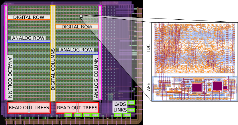
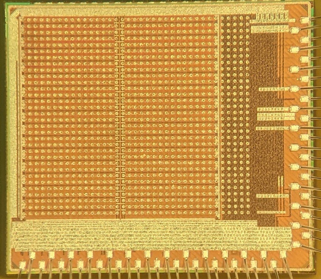
The Timespot1 ASIC is designed to provide a readout array suitable for chip-to-chip bump-bonding with 3D pixel arrays with a pixel size of . It integrates channels, organized in a matrix, with each channel equipped with its own Analog Front-End (AFE) and TDC. The block architecture is shown in Figure 1, while Figure 2 shows the full layout of the chip, featuring metal levels.
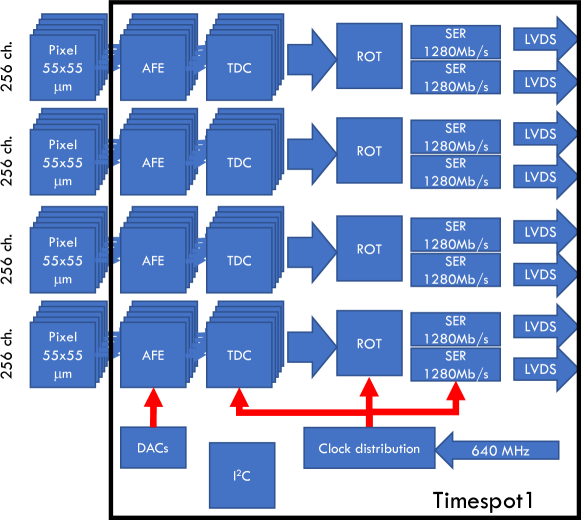
The input channels are organized in two blocks of 512 pixels, each consisting of 2 groups of 256 channels. Each group is connected to one out of four Read Out Tree (ROT) blocks. Each ROT collects data from the active channels, assigns them a global timestamp and sends formatted data to one of the two serializers connected to LVDS drivers. In total, 8 LVDS drivers are integrated, sustaining a data rate of each, with an overall maximum data throughput of .
From the floorplan point of view, the array is arranged in two mirrored pixels blocks. The size of each channel is , therefore the pitch is reduced in the horizontal direction compared to the bond-pad matrix. A redistribution layer is used to connect each channel to its own bond-pad. In this way, are saved every 16 pixels in order to be used for distribution of analog references and power supplies on one side (Analog Column), and for digital power supplies and data transmission lines on the other side (Digital Column). Particular care was used to maintain as separate as possible the digital domain from the analog one. In particular, the analog part of the channels was integrated in an Analog Row with its own substrate bias and power nets, connected only with the Analog Column. In the same way the digital part (TDC and control logic) is confined in its dedicated area (Digital Row), which is connected only with the Digital Column. In this way Analog and Digital domains are kept independent.
Particular attention was paid in regard to the coupling between the sensor and the pre-amplifier, since the redistribution scheme would create differences in the interconnection paths. The individual interconnection wires have been optimized in order to control their parasitic capacitance. The total capacitance due to the sensor together with the bond pad is below , therefore the small capacitance differences (of the order of a few femto-Farad) due to the differences in the interconnections, can be neglected.
The readout scheme is totally data-driven and trigger-less, with time-stamping from an externally provided signal. Timespot1 also integrates structures for internal services , such as two voltage bandgaps and 8 DACs for Voltage references.
The chip configuration is handled using a slow-control interface I2C-like protocol [27].
3.1 Analog Front-End

A schematic representation of the Analog Front-End (AFE) [28] is shown in Figure 3. Each channel is made of a Charge Sensitive Amplifier (CSA) as first stage and a leading edge discriminator as second stage. Additionally, each CSA is both connected to the respective sensor bond-pad and to its own charge-injection circuit. This last block is used to generate current test pulses to be used during electrical self-tests. The total area is which also includes the required digital buffers and decoupling capacitors.
The CSA is a trans-impedance stage which produces output voltage signals proportional to the integrated charge of the input current signals. In terms of jitter performance a key parameter is the total capacitance coupling the input and output nodes of the CSA. The direct effect is connected to the fact that the output signal slew-rate is inversely proportional to this capacitance. Therefore, this total capacitance must be minimized. For this reason, no additional capacitor was added in feedback, leaving only the parasitic capacitance coupling the two nodes. The capacitance value is estimated using a parasitic extraction method to be around . The CSA consists in a Core Amplifier (CA) and a Krummenacher filter [29].
The function of the CA is to charge the feedback capacitance. The output noise and bandwidth of this block are critical to enhance the signal time accuracy. In fact, the time jitter of the pre-amplifier stage can be quantified by the ratio between its signal noise and slew-rate. These characteristics are all tied to the available power, therefore it is critical to maximize the architecture performance for a power consumption under a constrained power budget of . Moreover, in the CSA configuration, the core amplifier open loop gain masks the stage input capacitance which makes possible to obtain higher slew-rates with the same power. The block has been implemented using a single inverter-like stage. Compared to a single input transistor stage, this architectures provides double the transconductance with the same bias current. In order to boost the open loop gain of the architecture, the two transistors have been cascoded. A challenging aspect of a linear inverter-based amplifier is the proper biasing of its DC operating point. In particular, it is difficult to force a reliable DC input voltage while also forcing the desired bias current in the stage. To achieve this, the NMOS input has been AC coupled to the PMOS , splitting the DC voltages of the two transistors. These two nodes are then biased using two separate feedback paths.
The two feedback circuits are implemented using two complementary realizations of the Krummenacher filter in order to have the best DC matching. The NMOS variant is used to bias the PMOS input, while the PMOS one is used for the NMOS input. The feedback paths are also responsible for the discharge of the feedback capacitor. In particular, this architecture features a constant current discharge which creates a proportionality between the input charge and the output signal ToT. The discharge current value is programmable and can be set between and . Additionally, this architecture is also able to compensate the sensor leakage current up to values around to its discharge current: up to .
The discriminator produces the digital pulses which are used as the TDC input. These pulses must retain the timing properties of the analog signals. The CSA signal is compared to a given voltage threshold, producing a steep digital step when the input exceed the threshold. The core of this block is implemented with a two stage open loop amplifier with differential input. The first differential stage is used to compare the signal and the threshold. The second single ended stage is used to boost the voltage gain bringing the total gain of the discriminator core to .
In order to produce a reliable discrimination across the channels, the effective threshold variation must be accounted for. This is usually carried out with a per-pixel threshold calibration. Due to the required precision and available pixel area this approach is unfeasible for this application. The threshold offset was corrected dynamically with a discrete-time offset-compensation circuit. The Offset Compensation (OC) procedure allows equalizing the CSA output DC levels, and compensating the discriminator offset. This feature is implemented by AC-coupling the CSA output with the discriminator input using the capacitor (Figure 3), and by inserting a switching circuit between the signal terminal and the output of the inverting amplifications stage, thus creating a negative feedback loop. During the OC the discriminator is closed in an almost-unitary loop. In this condition the voltage developing at its threshold terminal is saved in the capacitor . This voltage will act as the signal baseline level. By reopening the feedback the discriminator is again able to process the incoming signals. The actual threshold can now be applied to the threshold terminal: its value will be relative to the saved baseline. From a system-level point of view, this procedure requires only a common voltage level shared among the channels. Each channel must only include its own digital control signals.
The baseline value will tend to drift away from the stored one due to the presence of parasitic currents, discharging . Therefore the OC procedure must be repeated periodically. The frequency of this operation and the time required to perform it will determine a dead time for the channel. and the feedback switch have been sized in order to optimize the circuit dead time. Specifically, the sizing of constitutes a trade-off between the the OC coherence time and a low pass filtering by the mean of its parasitic capacitance to ground. Its capacitance value has been set to . The switch has been sized acting on its in order to reduce it off-current and therefore its on-current. This creates a trade-off between the OC setting time and its coherence. As result the circuit is able to achieve a setting time, with a coherence time of corresponding to a dead time of . This result was measured on a previous prototype [30].
Finally, after the core discriminator, the signal is buffered with a CMOS inverter in order to produce a digital pulse.
3.2 TDC

The TDC measures the Time of Arrival (TA) of the AFE signal, in terms of its phase with respect to a reference clock running at 40 MHz. At the same time the TDC measures the Time Over Threshold (ToT) of the signal to correct the signal Time Walk to improve the TA measurement (Figure 4). The ToT resolution will define the granularity of the TA correction, which in turn will affect the overall detector resolution. The minimum required resolution for the ToT has been evaluated based on the expected AFE TA versus ToT relation to be rms.
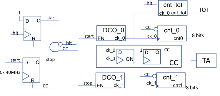
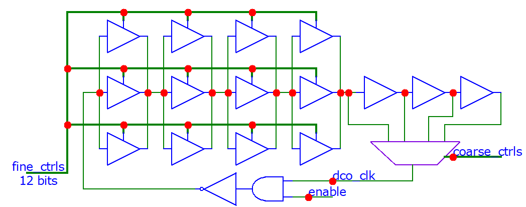
The TDC is based on a Vernier architecture [31], with two identical Digital Controlled Oscillators (DCOs) working at slightly different frequency (DCO_1 is faster than DCO_0) (Figure 5). The DCOs are made with a tapped delay line with tunable length (Figure 6). Each of the first four DCO step elements is made with three different tri-state buffers in parallel, each one with different drive strength. The fine delay is tuned by enabling one of them at a time. The last three stages are fixed delay cells and they are used for coarse adjustment. Each DCO drives an 8 bit fast counter. When in stand-by, both DCO’s are stopped, saving power. The signal edge starts the first DCO, whereas the second is started by the next reference clock edge. A Coincidence detect Circuit (CC) is used to detect when the two positive edges rise at the same time, indicating the end of measurement. A third counter is driven by the first DCO to calculate the signal ToT.
The TA is computed using:
| (3.1) |
where and are the periods of the two DCO’s while and are the related counter values. The theoretical resolution of a Vernier TDC is given by the period difference:
| (3.2) |
The conversion time for a Vernier architecture is not fixed and can be different for each measure. The maximum conversion time is given by:
| (3.3) |
where is given by the (3.2).
DCOs are calibrated at the beginning, independently for each pixel, to set the resolution and all the parameters needed to calculate the time. The calibration process is not aimed to fix precisely the DCOs frequencies, i.e. using some reference signal, but it sets the period difference () between the two DCOs to be consistent with the required resolution. Fixing the difference, instead of a given frequency, makes the system more stable with respect to the environment dependent variables like temperature. . At the end of calibration process, the working periods of the two DCOs ( and ) are stored on registers inside each pixel for TA calculation according to (3.1). The full calibration, completely managed internally to the pixel, needs less than to be completed and it is performed in two steps:
-
1.
The DCO_0 (the slowest) is set to generate a clock period around . The logic sets the DCO_0 with the slowest settings and activates it calculating the period. If the period is much higher than , the logic act on the coarse setting (Figure 6), reducing the length and consequently the period, and performing a new try.
-
2.
The DCO_1 (the fastest) is set to have a period slightly smaller than the DCO_0, according to the required resolution. The period is set iteratively while monitoring the period difference until the desired one is met. The used for the results on this paper is fixed around , which therefore corresponds to a theoretical LSB of .
During testing the periods of the DCOs obtained from the calibration showed good stability. By repeating the calibration over time, the variation of the periods always remained in the order of a few ps.
The TA value, expressed in , is calculated internally according to (3.1). The ToT is simply measured by counting the number of DCO_0 oscillations occurring while the input pulse is active. Both measurements require a time that cannot be foreseen a priori. With DCO period values around and a in the order of , using the 3.3 we obtain a of . The maximum ToT expected is . To avoid having to add a pixel-level timestamp, consequently increasing the data to be transmitted, the TDC works with a fixed latency, and the data is published and transmitted after a fixed time, large enough to guarantee the completion of the measurements, both for TA and ToT. The fixed latency determines the dead time of the TDC, and consequently the TDC maximum sustainable rate, which turns out to be .
The TDC data output includes both TA and ToT measurements. The TA measurement is expressed in ps and, having to cover a dynamic range of , requires a word. The ToT is calculated in terms of the number of cycles of the DCO_0 clock, whose period is fixed at about during the calibration phase. Having to cover a range up to , it requires an word. TDC data are output serialized at .
For debug purpose it is possible to send out the counter values ( and ) instead of the TA calculated internally.
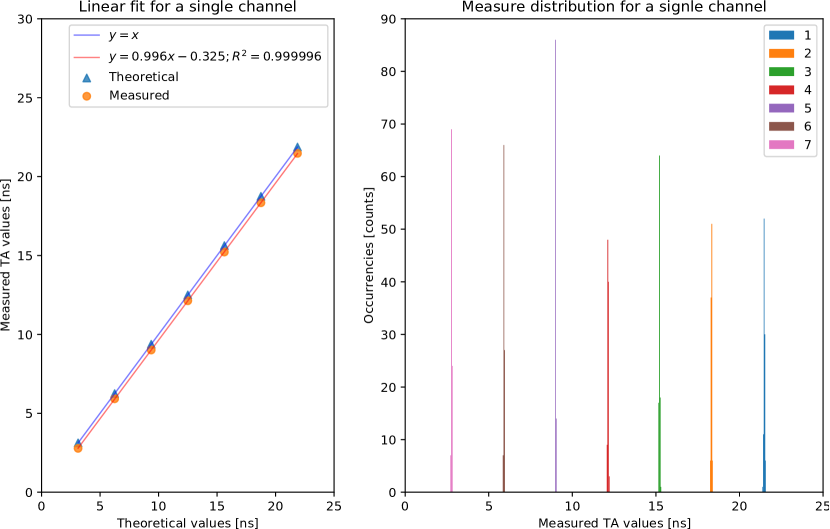
Furthermore, the TDC is able to self-generate test pulses to verify the TA measurement (with 7 different phases) and ToT measurement (with 32 different widths). The seven Test Point (TP) are generated on both clock edges (Figure 7), giving a well known Time Interval to be tested, equally distributed in step of over the dynamic range. Using these 7 points we can test the TDC to get an indication of its linearity and any INL problem. We can also study the distribution of repeated measures by calculating the standard deviation for each test point.

Table 3 summarizes the TDC characteristics and performance. Resolution and power consumption are related to post-layout simulations. Although in the IDLE condition the DCOs are switched off, the different service structures, such as the configuration and the services for the AFE circuit are active and contribute to the consumption. Some of these structures can be shared between different TDCs, thus contributing to a further reduction in overall consumption. This will be implemented in a following release.
| Size | |
|---|---|
| Max Event Rate | |
| Output Word | 24bits Serial @ |
| TA best bin size | |
| TA bin size used for prototype test | |
| ToT resolution | |
| PWR in IDLE | |
| PWR @ Event Rate |
3.3 Readout processing logic
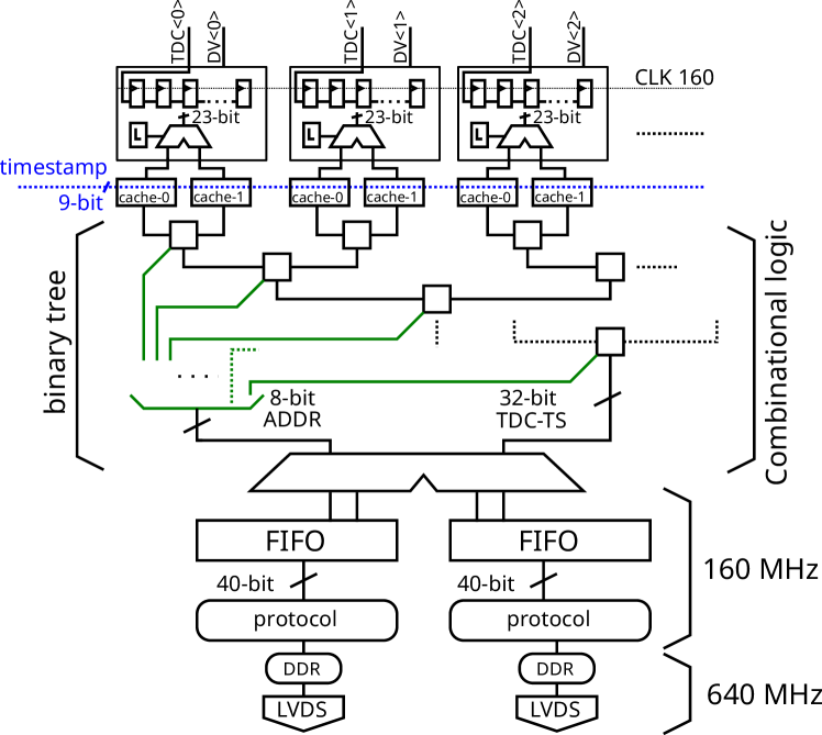
Each TDC is connected throughout the Digital Column via its dedicated serial line and its corresponding Data Valid (DV) signal to the readout processing logic. At every hit, the TDC sends its word, and activates the DV signal. Figure 8 shows the block diagram of the readout processing logic that contains the binary tree and the data serialization circuit. This block receives data from TDCs.
Each hit-data coming from the TDC is paired with the corresponding timestamp information () that indicates the sequential number of a counter on the clock when the hit data is generated. This counter is started using a dedicated external signal. The timestamp information is added at this point since the successive logic does not have a fixed latency. The data is then cached in order to reduce the risk of data-loss. While data are stored into the cache memories, a combinational binary tree [32] sequentially reads the data from the caches at a rate of and frees them. The binary tree generates the geographical coordinates of the pixel () and implements a zero-suppression feature.
The output of the binary tree consist of: address, TDC data and timestamp information. The resulting string is fed to one of two -word-deep FIFO’s, working at . The FIFOs are used to mitigate activity peaks that otherwise could cause data loss. The output of the FIFO is encoded using a custom transmitting protocol. The protocol is organized in words and it is constructed as follows: when data is present at the FIFO output, it is divided in five bytes preceded by a header byte, otherwise an idle byte is transmitted. The idle and header words can be chosen and set using the slow control.
The protocol block outputs a new byte at a frequency of . Each byte is then serialized with a Double Data Rate (DDR) and transmitted to the output using an LVDS protocol at . The maximum output bandwidth of Timespot1 is defined by the 8 LVDS cumulative bandwidth, resulting in . The per-channel sustainable hit-rate by the read out processing logic ranges from to depending on the channel occupancy. The first value corresponds to a single active pixel whereas the second ones correspond to a totally uniform hit occupancy (all channels firing at the same time).
4 Chip Measurements
4.1 Setup and Methods
Figure 9 shows a microscope photograph of the Timespot1 die, after wire-bonding on the test board.
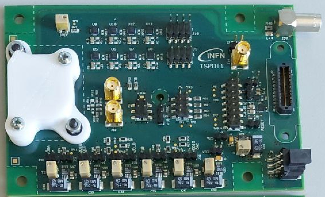
Timespot1 is being tested concerning its operation and circuit performance on a dedicated Printed-Circuit Board, named TSPOT1 (Figure 10). The tests illustrated in this paper where performed on the front-end chip alone, before hybridization with the sensor. The TSPOT1 is conceived to have the maximum possible access to the ASIC I/O, allowing the possibility to input and then visualize the signals by means of a pattern generator and a high-performance logic analyzer or oscilloscope. The same board can be used with a high-performance readout board, based on a Xilinx Kintex7 FPGA.
The test is performed using internal test pulses on individual channels. The TDC is tested after performing the Vernier’s DCO calibration. TA and ToT are verified using the self-generated test pulses, whereas the Front-End is tested using a test pulse generated internally with a fixed phase to the clock.
4.2 TDC Characterization
The TDC is characterized by its TA resolution , which is the most critical parameter for the timing performance. In particular , represents the total TDC resolution which the main contributions comes from the quantization error, the measurement process uncertainty and the reference clock stability. This last contribution has been evaluated using a loop-back configuration on the input clock driver. Its rms jitter has been evaluated to be around at the chip input. However, the stability will degrade along the clock path. A punctual evaluation of the clock stability is not measurable, therefore this value must be taken as an indication of its lower bound. The ToT has an LSB of about which meets the performance required to adequately apply the ToT correction.
The first tests concerned the study of the linearity of the TDC response. This is done by pulsing the single TDC repeatedly with the 7 test points which are evenly spaced inside the dynamic range. At the end of the test, the fit line is calculated. The slope of this line, together with the standard deviation of the individual measurements with respect to the line and the coefficient of determination (), provides us with a good indication of the linear response of the TDC and its INL. In Figure 11 we can see a tipical TA scan result for a single channel. On the left we have the linearity response, with the equation of the line fitting the data, with the coefficient of determination . In this plot we can also see a shift with respect to the theoretical straight line. This is expressed by the intercept value of the line which is non-zero. This is an expected phenomenon and due to a delay in the ignition system, which results in a systematic displacement of the points. Histograms of repeated measurements on each point are also built in order to evaluate the error associated to each performed phase measurement, as shown on the right plot of Figure 11.
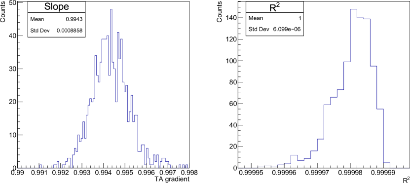
The test is extended to all the channels, to evaluate the uniformity around the matrix, and also to identify faulty channels. Figure 12 shows the results of linearity response of all channels. From this plots were excluded the channels not working. On the left we have the resulting slope distribution, while on the right we can see the coefficient of determination () distribution.
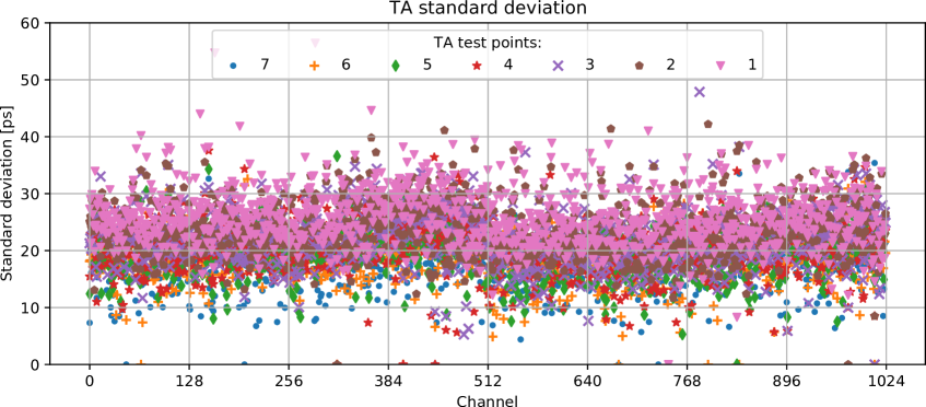
Figure 13 shows the scatter plot of the across all channel and phases, the phase and position dependencies can be observed in this plot. The plot shows a good uniformity across all matrix, with a small geometry effect on the right sub-matrix (after channel as shown in Figure 2). The plot also shows that TDC tends to perform slightly better for lower phase pulses.
4.3 Analog Front-End Characterization
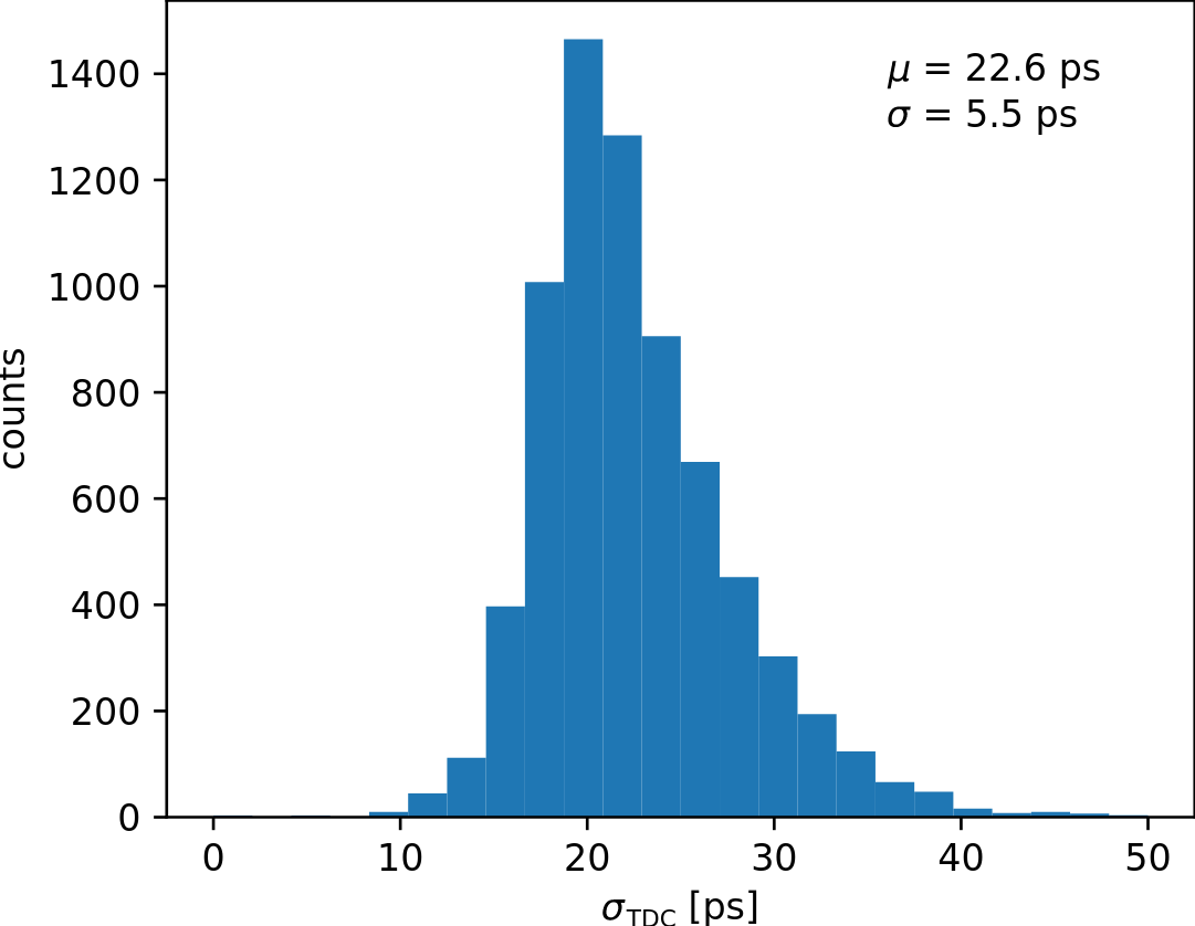
In the Timespot1 ASIC, the only method to measure the AFE output is by taking advantage of the channel TDC. Each AFE channel can be individually pulsed using its charge injection circuit. In response to this signal the AFE will produce a digital pulse which is then measured by the TDC. Consequently, with a single measurement, it is only possible to measure the TA and ToT of a signal. In order to extract more information, the channel can be statistically investigated by repeatedly pulsing the same channel. In this way the output signal jitter for a given condition can be evaluated as the standard deviation of TA measurement set (). The AFE component can be evaluated by removing the previously measured TDC contribution . This can be computed under the hypotheses that the two sources of variation are independent using:
| (4.1) |
Contrary what is natural to expect, values of smaller then can be measured. This case can be explained as an effect of a too small statistics: given the small difference to be measured in these specific cases, a larger statistical set is required to distinguish it compared to the cases with a larger .
In terms of the analog power consumption, the system can be finely configured by setting the bias currents on a per-block basis. The values of the configuration steps have been verified by directly measuring the analog current intake using a source meter directly connected to the analog power net. This measurement are inline with what expected in simulation. The following measurements were performed with a power consumption of per channel. This value includes the static power consumption of all the analog circuits in the pixel and the periphery, averaged for the number of pixels.
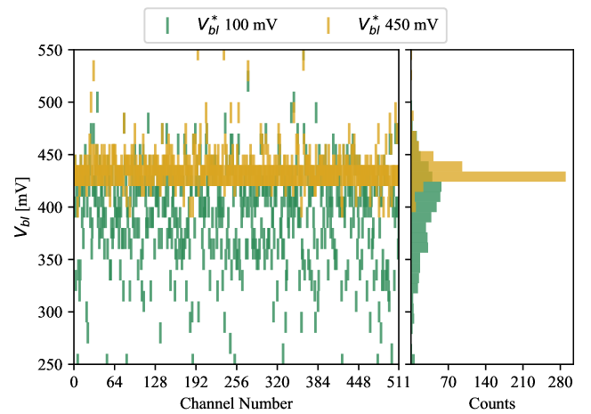
Moreover it is possible to reconstruct the CSA signal using a threshold-scan. During this analysis an issue with the OC was found: the OC has proven to be not able to compensate baseline fluctuations for low voltages. Figure 15 shows the baseline positions spread across a half matrix. The actual baseline position for each channel has been extracted from the threshold scan reconstruction, ant it has been defined as the level in which the signal starts forming. The analysis was performed with two desired baseline values , this voltage is the one provided by a global DAC on the discriminator threshold terminal. This problem might be caused by an incorrect setting of the voltages on the discriminator threshold terminal.
The correct OC procedure operation has already been verified in the previous prototype [33]. The only difference in the implementation of the discriminator between the two prototypes is the switching circuit. In the current implementation the circuit has been changed to use p-type switches since they have proven to be more radiation resistant [6]. Simulation shows that the transistor forming the switch on the threshold terminal is not in conduction regime whenever a low voltage is applied. In this condition the node is biased by its source-bulk current to a value around , similar to the one found in the analysis of Figure 15.
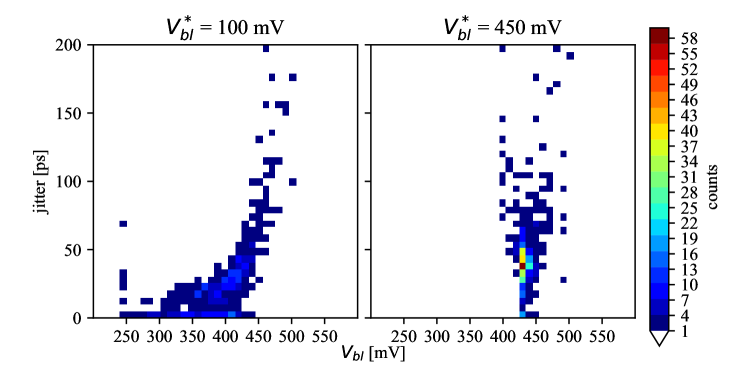
However the OC is still working properly for high values. The side effect of imposing a high-baseline is related to the fact that the threshold value must be set to an even higher value in order to measure signals with positive polarity. In this range, the p-type input discriminator will not operate at its optimal common mode voltage, thus limiting its bandwidth. This behavior is shown in Figure 16 in which is correlated to the measured baseline . When the OC is not working properly a correlation between and can be observed. Moreover, when the OC is set to high values, the compensated channels will feature the same which was found with the corresponding baselines in the previous case. These two facts suggest that the discriminator core is band-width limited for the high DC operating points: in this condition the biasing transistor of the differential pair drains a lower current than the desired one. This behavior has been verified in simulation.
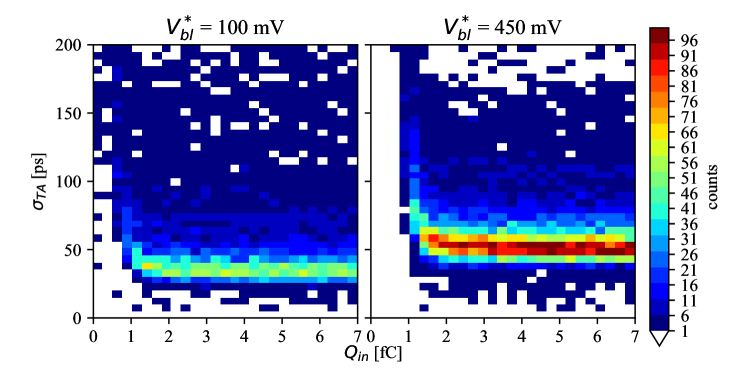
In such conditions, the AFE time resolution has been evaluated for a signal when the OC is working properly. This resulted in an average of for with a power consumption around per channel. However, if the hypothesis of the discriminator malfunction is true, the CSA should be able to reach a resolution better than .
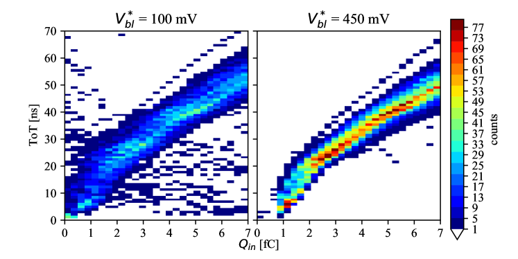
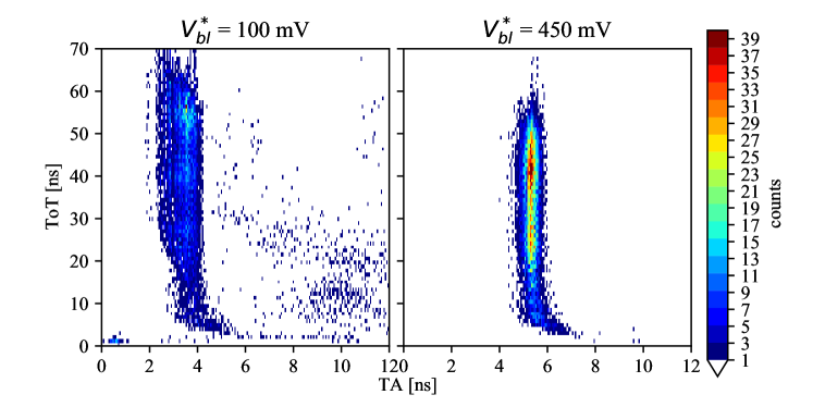
Another important characterization of the AFE is its performance for different input charges. Figure 17 shows for different input charges. Figure 18 shows the ToT linearity. Finally, Figure 19 reports the relation of the signal TA and its ToT. This relation is useful to correct the time-walk effect. It can be observed in each case that the issue with the OC is present for low baselines. As expected, the correct operation of the OC improves the per-channel signal variation.
5 Conclusions
The characterization of the Timespot1 ASIC has been presented. Timespot1 is the first CMOS ASIC designed and fabricated for the readout of pixel matrices with high-resolution timing capabilities per pixel. Still on a reduced size of pixels, with a pitch, it implements the full set of functionalities needed for the purpose of 4D tracking.
The Timespot1 AFE is capable of an average time resolution of , with a measured dispersion across the pixel matrix of about . The TDC has an average time resolution of and a dispersion of .
The measured AFE performance is affected by an identified design bug, causing the Offset-Compensating procedure to be inadequate for proper offset compensation when the threshold is set to low values. Once this bug is corrected, the performance of the AFE should be capable of a resolution of the order of or below. On the other hand, given the TDC bin size of around , the TDC quantization error of approaches the supposed clock stability. It is reminded that is value is greater than , making it a limiting factor for the overall resolution. Therefore the resolution can be significantly improved after a more accurate clock distribution across the matrix area.
The ASIC has been recently hybridized on 3D-trench silicon sensors [4] featuring a pixel matrix with matched geometry. Using the same TSPOT1-PCB, the hybrid is being tested stand-alone in the laboratory, stimulated by an IR pulsed laser source. Finally, the TSPOT1-PCB, equipped with the hybrid, will be used as a layer in a tracking telescope in test-beams with MIPs.
In the meantime, the design of a new version, featuring a larger pixel matrix of or pixels and improved timing performance is near to start. Such a large area matrix will be based on the current matrix, which is intended to be easily duplicated and repeated. To overcome the typical problems of large area matrices related to power distribution, it is thought to use the Through Silicon Vias (TSV), in order to distribute the power more punctually, reducing the power drops. Also the use of TSV can improve the distribution of the clock reducing the jitter on the clock linked to its distribution inside the chip, thus allowing to increase the temporal resolution achievable.
References
- [1] M. van Beuzekom et al., Vertex detector for LHCb Upgrade-II, in JPS Conf. Proc., vol. 34, p. 010014, 2021.
- [2] A. Lai, A system approach towards future trackers at high luminosity colliders: the TIMESPOT project, in IEEE Nuclear Science Symposium and Medical Imaging Conference Proceedings (NSS/MIC), pp. 1–3, 2018, DOI.
- [3] A. Lai, L. Anderlini, M. Aresti, A. Bizzeti, A. Cardini, G.-F. Dalla Betta et al., First results of the TIMESPOT project on developments on fast sensors for future vertex detectors, Nucl. Instrum. Meth. A 981 (2020) 164491.
- [4] L. Anderlini, M. Aresti, A. Bizzeti, M. Boscardin, A. Cardini, G.-F. Dalla Betta et al., Intrinsic time resolution of 3D-trench silicon pixels for charged particle detection, J.Instrum. 15 (2020) P09029.
- [5] D. Brundu, A. Cardini, A. Contu, G. Cossu, G.-F. Dalla Betta, M. Garau et al., Accurate modelling of 3D-trench silicon sensor with enhanced timing performance and comparison with test beam measurements, J.Instrum. 16 (2021) P09028.
- [6] C.-M. Zhang, F. Jazaeri, G. Borghello, S. Mattiazzo, A. Baschirotto and C. Enz, Bias dependence of total ionizing dose effects on 28-nm bulk MOSFETs, in IEEE Nuclear Science Symposium and Medical Imaging Conference Proceedings (NSS/MIC), pp. 1–3, 2018, DOI.
- [7] M. Krohn, B. Bentele, D. Christian, J. Cumalat, G. Deptuch, F. Fahim et al., Radiation tolerance of 65 nm cmos transistors, Journal of Instrumentation 10 (2015) P12007.
- [8] S. Bonacini, P. Valerio, R. Avramidou, R. Ballabriga, F. Faccio, K. Kloukinas et al., Characterization of a commercial 65 nm cmos technology for slhc applications, Journal of Instrumentation 7 (2012) P01015.
- [9] T. Ma, S. Bonaldo, S. Mattiazzo, A. Baschirotto, C. Enz, A. Paccagnella et al., Tid degradation mechanisms in 16-nm bulk finfets irradiated to ultrahigh doses, IEEE Transactions on Nuclear Science 68 (2021) 1571.
- [10] The CMS Collaboration, Technical proposal for a MIP timing detector in the CMS experiment Phase 2 upgrade, Tech. Rep. CERN, Geneva, Switzerland (Nov., 2017).
- [11] The ATLAS Collaboration, High-granularity timing detector for the ATLAS Phase-II upgrade, Technical Proposal CERN, Geneva, Switzerland (July, 2018).
- [12] The LHCb Collaboration, Framework TDR for the LHCb upgrade II: Opportunities in flavour physics, and beyond, in the HL-LHC era, Tech. Rep. CERN, Geneva, Switzerland (Feb., 2022).
- [13] The KOTO, LHCb, and NA62/KLEVER Collaborations, and the US Kaon Interest Group, Searches for new physics with high-intensity kaon beams, Apr., 2022. 10.48550/ARXIV.2204.13394.
- [14] T.S. Niknejad, Results with the TOFHIR2X revision of the front-end ASIC of the CMS MTD barrel timing layer, Tech. Rep. CERN, Geneva, Switzerland (Dec., 2021).
- [15] O.A. de Aguiar Francisco, W. Byczynski, K. Akiba, C. Bertella, A. Bitadze, M. Brock et al., Microchannel cooling for the LHCb VELO upgrade I, Nucl. Instrum. Meth. A 1039 (2022) 166874.
- [16] C. Riegel, M. Backhaus, J.V. Hoorne, T. Kugathasan, L. Musa, H. Pernegger et al., Radiation hardness and timing studies of a monolithic TowerJazz pixel design for the new ATLAS Inner Tracker, Journal of Instrumentation 12 (2017) .
- [17] S.I. Parker, C.J. Kenney and J. Segal, 3D – A proposed new architecture for solid-state radiation detectors, Nucl. Instrum. Meth. A 395 (1997) 328.
- [18] X. Llopart, J. Alozy, R. Ballabriga, M. Campbell, R. Casanova, V. Gromov et al., Timepix4, a large area pixel detector readout chip which can be tiled on 4 sides providing sub-200 ps timestamp binning, J. Instrum. 17 (2022) C01044.
- [19] J. Braach, E. Buschmann, D. Dannheim, K. Dort, T. Kugathasan, M. Munker et al., Performance of the FASTPIX sub-nanosecond CMOS pixel sensor demonstrator, Instruments 6 (2022) .
- [20] “FAST2: a new family of front-end ASICs to read out thin Ultra-Fast Silicon detectors achieving picosecond time resolution.” https://indico.cern.ch/event/1019078/contributions/4443951/, 2021.
- [21] “FastIC: A Fast Integrated Circuit for the Readout of High Performance Detectors.” https://indico.cern.ch/event/1019078/contributions/4443966/, 2021.
- [22] A. Ghimouz, F.E. Rarbi and O. Rossetto, DIAMASIC: A multichannel front-end electronics for high-accuracy time measurements for diamond detectors, 2021. 10.48550/ARXIV.2110.12440.
- [23] H. Sun, D. Gong, W. Zhang, C. Edwards, G. Huang, X. Huang et al., Characterization of the CMS endcap timing layer readout chip prototype with charge injection, Journal of Instrumentation 16 (2021) P06038.
- [24] C. Agapopoulou, P. Dinaucourt, A. Dragone, D. Gong, C. de La Taille, N. Makovec et al., ALTIROC 1, a 25 ps time resolution ASIC for the ATLAS high granularity timing detector, in IEEE Nuclear Science Symposium and Medical Imaging Conference (NSS/MIC), pp. 1–4, 2020, DOI.
- [25] “Precision timing ASIC for LGAD sensors based on a Constant Fraction Discriminator – FCFD0 .” https://indico.cern.ch/event/1019078/contributions/4443948/, 2021.
- [26] G. Aglieri Rinella, S. Bonacini, P. Jarron, J. Kaplon, A. Kluge, M. Morel et al., The TDCpix ASIC: High rate readout of hybrid pixels with Timing Resolution Better than 200 ps, in 2013 IEEE Nuclear Science Symposium and Medical Imaging Conference (2013 NSS/MIC), pp. 1–4, 2013, DOI.
- [27] “I2C-bus specification and user manual.” https://www.nxp.com/docs/en/user-guide/UM10204.pdf, Oct., 2021.
- [28] L. Piccolo, An Analog Pixel Front-End for High Granularity Space-Time Measurements, Ph.D. thesis, Politecnico di Torino Electrical, Electronics and Communications Engineering, 2022.
- [29] F. Krummenacher, Pixel detectors with local intelligence: an IC designer point of view, Nucl. Instrum. Meth. A 305 (1991) 527 .
- [30] L. Piccolo, First measurements on a discrete-time front-end in 28-nm cmos technology for timing pixel detectors, in 2019 IEEE Nuclear Science Symposium and Medical Imaging Conference (NSS/MIC), pp. 1–4, 2019, DOI.
- [31] R.G. Baron, The vernier time-measuring technique, Proc. of the IRE 45 (1957) 527 .
- [32] P. Fischer, First implementation of the MEPHISTO binary readout architecture for strip detectors, Nucl. Instrum. Meth. A 461 (2001) 499.
- [33] L. Piccolo, First measurements on a discrete-time front-end in 28-nm CMOS technology for timing pixel detectors, in IEEE Nuclear Science Symposium and Medical Imaging Conference (NSS/MIC), pp. 1–4, 2019, DOI.