Energy transfer from tunneling electrons to excitons
Abstract
Excitons in optoelectronic devices have been generated through optical excitation, external carrier injection, or employing pre-existing charges. Here, we reveal a new way to electrically generate excitons in transition metal dichalcogenides (TMDs). The TMD is placed on top of a gold-hBN-graphene tunnel junction, outside of the tunneling pathway. This electrically driven device features a photoemission spectrum with a distinct peak at the exciton energy of the TMD. We interpret this observation as exciton generation by energy transfer from tunneling electrons, which is further supported by a theoretical model based on inelastic electron tunneling. Our findings introduce a new paradigm for exciton creation in van der Waals heterostructures and provide inspiration for a new class of optoelectronic devices in which the optically active material is separated from the electrical pathway.
Exciton generation in TMDs
Transition metal dichalcogenides (TMDs) have attracted attention due to their interesting electronic and optical properties. In monolayer form, they exhibit a direct bandgap [1], responsible for radiative electron-hole recombination [2]. TMDs support excitons with high binding energies due to quantum confinement [3], making their optical properties to be dominantly defined by their excitonic states [4, 5, 6]. Exciton generation in TMDs was first studied through optical excitation [1, 7, 2, 8, 9, 10]. Later, combination with conductors (i.e. graphene) and insulators (i.e. hexagonal boron nitride) [11, 12] allowed the design and fabrication of light-emitting van der Waals (vdW) heterostructures with TMDs as the optically active material [13, 14, 15, 16, 17, 18, 19, 20, 21, 22, 23, 24, 25, 26, 27, 28]. In these studies, excitons are electrically generated through direct charge injection [13, 14, 15, 16, 17, 18, 19, 20, 21, 22, 23, 24, 25, 26, 27] or through charge impact at high alternating voltages [28]. Here, we introduce a different way to generate excitons in TMD based tunneling devices. We use the rich platform of 2D materials to demonstrate excitonic light emission from tunnel junctions where the TMD is located outside of the current pathway.
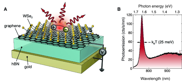
The studied device structure is illustrated in Fig. 1A. The TMD and the tunnel junction are electrically decoupled, preventing exciton generation through direct electron-hole injection. The emission spectrum of such a device features a distinctive peak at the exciton energy, as shown in Fig. 1B. We attribute the generation of excitons to energy transfer (ET) from tunneling electrons. ET from a donor to an acceptor is mediated by dipole-dipole coupling [29, 30]. It is an electromagnetic effect that is dominant at the near-field region of an emitter and has been extensively studied in biological systems [31], molecular assemblies [32], solid-state quantum dots [33] and photosynthetic membranes [34]. It has been also used for color conversion and broadband source design as an energy exchange channel between different fluorophores [35, 36]. Recent STM studies discuss the possibility of ET in tunneling systems [26, 27] without however providing any conclusive observation. Here we make use of atomically thin 2D materials and the flat interfaces between them to preserve optical coupling in near-field distances between a TMD and a tunnel junction. Our results reveal the role of ET between electrons and excitons in tunneling-based light emitting devices.
TMD-coupled tunnel junctions
Our devices are fabricated by stacking mechanically exfoliated flakes of 2D materials with a dry pickup and transfer technique (see supplementary materials for details). The resulting tunnel junctions consist of a graphene and a gold electrode separated by a hexagonal boron nitride layer (hBN) of thickness acting as a tunneling barrier. The TMD is stacked on top of the junction and optionally separated from the graphene electrode by a second hBN layer.
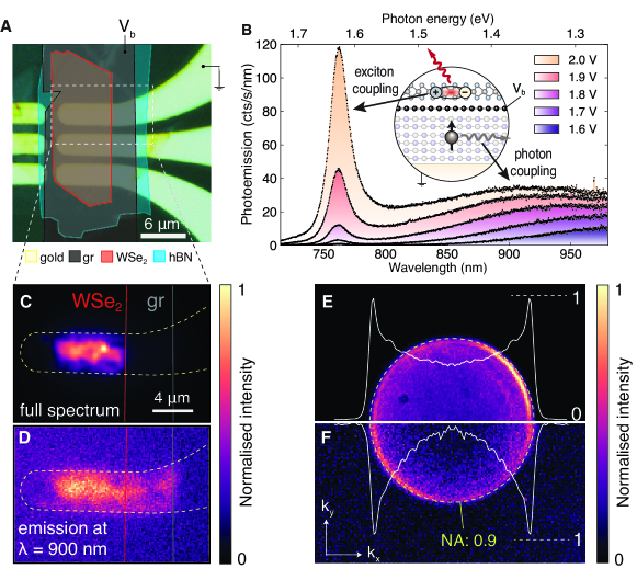
Figure 2A shows a false-color microscope image of the device with an outline of the different flakes. The device area is indicated by a white dashed box. The tunnel junction area is defined by the overlap of the gold electrode and the graphene flake. The WSe2 flake is only partially covering the tunneling area. This creates two different tunneling regions, with and without WSe2 on top. We electrically and optically characterize the device by applying a bias voltage () between the gold and graphene electrodes, as indicated in Fig. 2A, and we collect the emitted light with a high-numerical aperture objective (see supplementary materials). The current and conductance measurements suggest that tunneling occurs between graphene and gold (see Fig. S1A). The spectra emitted from the whole tunneling area for various values are presented in Fig. 2B. There are two distinct contributions in the spectra. A broad emission at lower energies and a narrow emission peak at (). The broad emission shifts to higher photon energies as is increased. This behavior suggests that the emission originates from inelastic electron tunneling that couples to radiative modes of the free-space continuum (photon-coupling) with e being the cut-off energy of emission [37, 38]. The narrow peak at corresponds to the neutral 1s exciton of WSe2 and its narrow width of around can be attributed to graphene filtering [39]. It has been shown that charge transfer between graphene and TMDs, filters the TMD photoluminescence spectra from any charged exciton contributions [39]. To further our understanding, we study the emission distribution for different spectral regions. Real space images of the photoemission are presented in Fig. 2C, where we observe that the area covered by WSe2 dominates the emission and in Fig. 2D, where the emission is filtered by a band-pass filter at . This is a spectral region where the excitonic contribution is much reduced and the emission extends over both device areas. This indicates that the broad low energy contribution indeed originates from photon-coupling and is not associated with the presence of WSe2. To understand the angular emission of the device we record Fourier-space images. Fig. 2E shows the Fourier space image of the full emission spectrum whereas Fig. 2F depicts the Fourier space image of the bandpass filtered light around . For the spectrally filtered measurement at 900 nm, the emission vanishes at the center of the Fourier space () (Fig. 2F) indicative for an out-of-plane dipole orientation. This is characteristic of inelastic electron tunneling where the transition dipole is oriented along the electron path. On the other hand, when measuring the full spectrum, the Fourier space image (Fig. 2E) is not zero at , which indicates an in-plane contribution. This extra contribution is associated with the excitonic emission of WSe2, which is known to originate from in-plane transitions [40]. We emphasize that in our devices any exciton generation due to electron-hole injection is avoided due to the WSe2 being outside of the tunneling pathway. This is further supported by the fact that very similar emission spectra are observed for negative (see Fig. S2). For these reasons we conclude that excitons are generated in the TMD by ET from tunneling electrons.
We continue to investigate this exciton generation process by considering the band-structure diagram shown in Fig. 3A. Upon application of , electrons tunnel from one electrode to the other, elastically or inelastically. In the latter case, the transition dipole associated with the energy loss couples to available optical modes of the environment. Some of these modes are radiative (photons) as in the case of the broad emission observed in Fig. 2A, or non-radiative, as in the case of ET. This ET mechanism generates excitons in WSe2 and their spontaneous decay contributes to the narrow emission peak in the spectra of Fig. 2B. Thus, the excitonic emission observed in our device is a two step process, in which the transition energy is first transferred to the WSe2 exciton and then spontaneously emitted (exciton-coupling).
Next, we compare the ET efficiency to the photon-coupling efficiency. To do that we first break down the processes to the involved interactions (see pictorial representation in Fig. 3B) and we assign conversion efficiencies. Both photon- and exciton-coupling processes describe an electron-to-photon () conversion. Photon-coupling is a first order process for which we define an conversion efficiency as . Exciton-coupling is a second order process in which we can assign a combined efficiency , where is the ET efficiency and is the exciton to photon conversion efficiency. From the spectra shown in Fig. 2B, we can infer a value of 4.3 for the ratio between the photon-coupled emission and the exciton-coupled emission. By taking into account the values for WSe2 PL efficiency and the graphene quenching (see supplementary materials) we arrive at an estimation of the ratio . This result indicates that ET is orders of magnitude more efficient than direct photon emission. In order to shed light on this surprising finding we analyze in the next section the density of optical states near a monolayer TMD.
Optical density of states near monolayer TMDs
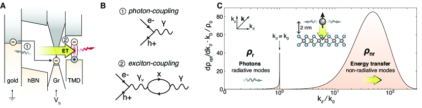
When a dipole interacts with an absorbing material at a distance much smaller than the wavelength, the largest fraction of the dissipated power is associated with non-radiative energy transfer (ET) from the dipole to the material [41, 42]. The rate of this process is related to the local density of optical states (LDOS) . In Fig. 3C we show the calculated angular spectral density of the LDOS, , as a function of for the simple case of a dipole at distance from a TMD monolayer. Here, is the wavevector component along the plane of the TMD monolayer (see inset in Fig. 3C) and is the wavenumber for a photon energy equal to the exciton energy of WSe2. The calculated for includes radiative modes associated with photon emission () whereas the region accounts for non-radiative modes () associated with ET. is orders of magnitude higher than . Moreover, the influence of the TMD on enhancement is negligible. Hence, the TMD introduces mainly additional non-radiative decay channels that are associated with near-field ET (), and is the reason for the high ratio. The ET process in our measurements is highly efficient and shows that near-field interactions at nanoscale distances are dominating the LDOS. Here, we probe this non-radiative interaction by using a direct-gap semiconductor whose luminescence is a direct measure for the ET efficiency. In essence, the TMD acts as a receiving optical antenna that enhances the LDOS and converts non-radiative modes to a measurable signal. We refer to this process as electron-photo-luminescence (ePL) since it is triggered by an electron that transfers energy through optical modes to WSe2.
Dependence on TMD-Graphene separation
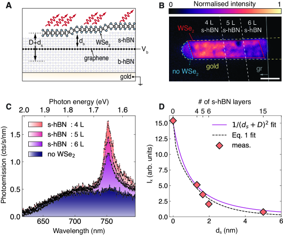
To further test our interpretation, we study the dependence of the excitonic emission on the distance between the TMD and the tunnel junction. A device schematic is shown in Fig. 4A where we vary the coupling to the TMD by changing the thickness of a hBN spacer layer (s-hBN) in different device regions. Figure 4B shows the emitted light from a device where the s-hBN presents steps in thickness in the tunnel junction area. Four regions of emission are created. Three with different s-hBN thicknesses (6, 5 and 4 layers) and one without WSe2 on top. We observe that the emission gets stronger the thinner the s-hBN is. As evidenced by the spectra shown in Fig. 4C the enhanced emission can be entirely attributed to the strength of the excitonic peak. We thus find that the excitonic contribution increases for thinner s-hBN in contrast to the broadband background that doesn’t show any major change. A comparison of the excitonic emission intensity for different at = is given in Fig. 4D. To compare different devices we normalize by the area of emission, the PL efficiency and the background level (see supplementary materials). The data points in Fig. 4D clearly show that the rate of exciton generation, and hence the ET rate, decay superlinearly with the separation .
can be modeled by calculating the exciton generation rate . By using inelastic tunneling theory [43] assumes the following expression:
| (1) | ||||
where is the angular frequency, is the absorption spectrum of monolayer WSe2 [7], is the inelastic tunneling spectral rate in vacuum and is the vacuum LDOS. We approximate the LDOS responsible for exciton generation by which assumes that the states provided by the TMD, leading to exciton generation, vanish for . See supplementary materials for more information on the calculation. The calculated as a function of distance and for = is plotted in Fig. 4D. It agrees well with the distance dependent measurement. Interestingly, both and the measured data can be described by a simple inverse square law, as shown in Fig. 4D. Similar observations were reported for ET between optically excited TMDs [44]. The good agreement between our theoretical model and our experimental measurements supports our interpretation.
Monolayer vs bilayer TMD
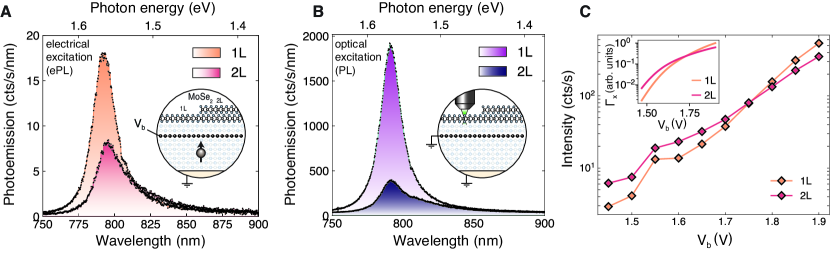
We continue our study by using a different TMD (MoSe2) and by comparing ET for monolayers (1L) and bilayers (2L). Figure 5A shows a schematic of the device and the measured ePL spectra. The emission for 2L MoSe2 () is less intense than for 1L MoSe2 () owing to the indirect bandgap of 2L MoSe2. To compare this ET-mediated photoluminescence (ePL) with optically excited photoluminescence (PL) we optically excite the two regions with a laser and measure the corresponding emission spectra and , respectively. The measurements are presented in Fig. 5B. The center wavelengths and the shapes of PL and ePL spectra match very well, which supports the interpretation that ePL corresponds to spontaneous exciton emission. We note however, that the ratios / and / are different. Interestingly, the / ratio depends on . In fact, is stronger than for low voltages and a crossing occurs near = , as shown in Fig. 5C, which depicts the integrated spectra for different voltages. By employing the model in Eq. 1 we are able to reproduce this effect. The result of this calculation is given in the inset of Fig. 5C. The reason for this voltage dependence are the different optical properties of 1L and 2L MoSe2, i.e. the absorption spectrum of 2L MoSe2, which features a cut-off energy at lower energies and stronger absorption than the 1L MoSe2. This explains the earlier onset-voltage for in Fig. 5C. Moreover, the two curves are also affected by the dependence of the LDOS on flake thickness. In fact, our model predicts that the rate of ET to a 2L TMD is lower compared to a 1L despite the fact that the 2L TMD is thicker. This surprising behavior has been studied in the past in optically excited systems [45].
Discussion
The exciton generation mechanism, discussed in this work, is an electromagnetic phenomenon that is usually neglected in the analysis of tunneling driven systems. The tunneling probability of an electron relies on the available electronic states but also optical states. In semiconducting materials, exciton resonances provide non-radiative optical states that couple strongly with inelastic electrons increasing the tunneling probability. This leads to near-field generation of excitons even for applied voltages below the electronic bandgap of the material, thus contributing to sub-bandgap emission. Such low voltage emission has been previously studied with interpretations varying from direct exciton formation [16] to Auger scattering [24]. Here we show that ET from tunneling electrons can contribute to this sub-bandgap emission.
Conclusions
We investigated ET from a tunnel junction to TMD excitons. Our studies are based on vdW tunnel devices in which the TMD is placed outside the electronic pathway, ensuring that there is no direct charge injection into the TMD. We studied photoemission spectra as well as real space and Fourier space emission patterns and we concluded that excitons are generated when the tunnel junction is under bias. This surprising observation is understood by ET from tunneling electrons to excitons. Emission from excitons is observed even when the TMD is separated from the junction by a hBN spacer layer. Our calculations reveal that non-radiative modes of the LDOS are strongly increased at the exciton energy. These non-radiative modes are responsible for the efficient energy transfer from the tunnel junction to the TMD. Our theoretical model based on inelastic tunneling theory and near-field coupling is in agreement with our experimental measurements.
The electrical generation of excitons via ET provides new perspectives for the development of optical sources, detectors and sensors. For example, it can be employed for truly chip-scale light sources with applications in electrical pumping scheme for vdW heterostructure lasers [46, 47] or optical sensing schemes [48] that do not rely on external laser sources.
Acknowledgments
The authors would like to thank Mathieu Luisier, Achint Jain, Martin Frimmer, Ronja Khelifa, Anna Kuzmina, Shengyu Shan and Massimiliano Rossi for fruitful discussions. This study was supported by funding from ETH Zurich under ETH Grant No. ETH-15 19-1 SYNEMA, the ETH Zurich Foundation project number 2013-08 (11) with a donation from the Stavros Niarchos Foundation, and the Swiss National Science Fund under grant number . K.W. and T.T. acknowledge support from the JSPS KAKENHI (Grant Numbers 19H05790, 20H00354 and 21H05233).
Author contributions
S.P., L.W. and L.N. conceived the experiment. S.P. fabricated the devices, performed the measurements, analysed the data, developed the theoretical model and performed the calculations. L.W. supported in the device fabrication. L.W. and L.N. helped with the data interpretation. K.W. and T.T. provided the high-quality hBN crystals, L.N. initiated and supervised the project. S.P. wrote the paper and all authors discussed the results and worked on the manuscript.
References
- Mak et al. [2010] K. F. Mak, C. Lee, J. Hone, J. Shan, and T. F. Heinz, Atomically thin MoS2: A new direct-gap semiconductor, Physical Review Letters 105, 2 (2010), 1004.0546 .
- Splendiani et al. [2010] A. Splendiani, L. Sun, Y. Zhang, T. Li, J. Kim, C. Y. Chim, G. Galli, and F. Wang, Emerging photoluminescence in monolayer MoS2, Nano Letters 10, 1271 (2010).
- Chernikov et al. [2014] A. Chernikov, T. C. Berkelbach, H. M. Hill, A. Rigosi, Y. Li, O. B. Aslan, D. R. Reichman, M. S. Hybertsen, and T. F. Heinz, Exciton binding energy and nonhydrogenic Rydberg series in monolayer WS2, Physical Review Letters 113, 10.1103/PhysRevLett.113.076802 (2014), 1403.4270 .
- Jung et al. [2018] G. H. Jung, S. J. Yoo, and Q. H. Park, Measuring the optical permittivity of twodimensional materials without a priori knowledge of electronic transitions, Nanophotonics 8, 263 (2018).
- Hsu et al. [2019] C. Hsu, R. Frisenda, R. Schmidt, A. Arora, S. M. de Vasconcellos, R. Bratschitsch, H. S. van der Zant, and A. Castellanos-Gomez, Thickness-Dependent Refractive Index of 1L, 2L, and 3L MoS2, MoSe2, WS2, and WSe2, Advanced Optical Materials 7, 10.1002/adom.201900239 (2019).
- Ermolaev et al. [2020] G. A. Ermolaev, Y. V. Stebunov, A. A. Vyshnevyy, D. E. Tatarkin, D. I. Yakubovsky, S. M. Novikov, D. G. Baranov, T. Shegai, A. Y. Nikitin, A. V. Arsenin, and V. S. Volkov, Broadband optical properties of monolayer and bulk MoS2, npj 2D Materials and Applications 4, 1 (2020).
- Kozawa et al. [2014] D. Kozawa, R. Kumar, A. Carvalho, K. Kumar Amara, W. Zhao, S. Wang, M. Toh, R. M. Ribeiro, A. H. Castro Neto, K. Matsuda, and G. Eda, Photocarrier relaxation pathway in two-dimensional semiconducting transition metal dichalcogenides, Nature Communications 5, 1 (2014).
- Lien et al. [2019] D. H. Lien, S. Z. Uddin, M. Yeh, M. Amani, H. Kim, J. W. Ager, E. Yablonovitch, and A. Javey, Electrical suppression of all nonradiative recombination pathways in monolayer semiconductors, Science 364, 468 (2019).
- Amani et al. [2015] M. Amani, D. H. Lien, D. Kiriya, J. Xiao, A. Azcatl, J. Noh, S. R. Madhvapathy, R. Addou, K. C. Santosh, M. Dubey, K. Cho, R. M. Wallace, S. C. Lee, J. H. He, J. W. Ager, X. Zhang, E. Yablonovitch, and A. Javey, Near-unity photoluminescence quantum yield in MoS2, Science 350, 1065 (2015).
- Kim et al. [2021] H. Kim, S. Z. Uddin, N. Higashitarumizu, E. Rabani, and A. Javey, Inhibited nonradiative decay at all exciton densities in monolayer semiconductors, Science 373, 448 (2021).
- Novoselov et al. [2005] K. S. Novoselov, D. Jiang, F. Schedin, T. J. Booth, V. V. Khotkevich, S. V. Morozov, and A. K. Geim, Two-dimensional atomic crystals, Proceedings of the National Academy of Sciences of the United States of America 102, 10451 (2005).
- Geim and Grigorieva [2013] A. K. Geim and I. V. Grigorieva, Van der Waals heterostructures, Nature 499, 419 (2013), 1307.6718 .
- Withers et al. [2015a] F. Withers, O. Del Pozo-Zamudio, A. Mishchenko, A. P. Rooney, A. Gholinia, K. Watanabe, T. Taniguchi, S. J. Haigh, A. K. Geim, A. I. Tartakovskii, and K. S. Novoselov, Light-emitting diodes by band-structure engineering in van der Waals heterostructures, Nature Materials 14, 301 (2015a).
- Paur et al. [2019] M. Paur, A. J. Molina-Mendoza, R. Bratschitsch, K. Watanabe, T. Taniguchi, and T. Mueller, Electroluminescence from multi-particle exciton complexes in transition metal dichalcogenide semiconductors, Nature Communications 10, 1 (2019).
- Peña Román et al. [2020] R. J. Peña Román, Y. Auad, L. Grasso, F. Alvarez, I. D. Barcelos, and L. F. Zagonel, Tunneling-current-induced local excitonic luminescence in p-doped WSe2monolayers, Nanoscale 12, 13460 (2020).
- Binder et al. [2017] J. Binder, F. Withers, M. R. Molas, C. Faugeras, K. Nogajewski, K. Watanabe, T. Taniguchi, A. Kozikov, A. K. Geim, K. S. Novoselov, and M. Potemski, Sub-bandgap Voltage Electroluminescence and Magneto-oscillations in a WSe2 Light-Emitting van der Waals Heterostructure, Nano Letters 17, 1425 (2017).
- Palacios-Berraquero et al. [2016] C. Palacios-Berraquero, M. Barbone, D. M. Kara, X. Chen, I. Goykhman, D. Yoon, A. K. Ott, J. Beitner, K. Watanabe, T. Taniguchi, A. C. Ferrari, and M. Atatüre, Atomically thin quantum light-emitting diodes, Nature Communications 7, 1 (2016), 1603.08795 .
- Jauregui et al. [2019] L. A. Jauregui, A. Y. Joe, K. Pistunova, D. S. Wild, A. A. High, Y. Zhou, G. Scuri, K. de Greve, A. Sushko, C. H. Yu, T. Taniguchi, K. Watanabe, D. J. Needleman, M. D. Lukin, H. Park, and P. Kim, Electrical control of interlayer exciton dynamics in atomically thin heterostructures, Science 366, 870 (2019).
- Sundaram et al. [2013] R. S. Sundaram, M. Engel, A. Lombardo, R. Krupke, A. C. Ferrari, P. Avouris, and M. Steiner, Electroluminescence in single layer mos2, Nano Letters 13, 1416 (2013).
- Ross et al. [2014] J. S. Ross, P. Klement, A. M. Jones, N. J. Ghimire, J. Yan, D. G. Mandrus, T. Taniguchi, K. Watanabe, K. Kitamura, W. Yao, D. H. Cobden, and X. Xu, Electrically tunable excitonic light-emitting diodes based on monolayer WSe2 p-n junctions, Nature Nanotechnology 9, 268 (2014).
- Uddin et al. [2022] S. Z. Uddin, N. Higashitarumizu, H. Kim, I. K. M. R. Rahman, and A. Javey, Efficiency Roll-Off Free Electroluminescence from Monolayer WSe 2 , Nano Letters 10.1021/acs.nanolett.2c01311 (2022).
- Withers et al. [2015b] F. Withers, O. Del Pozo-Zamudio, S. Schwarz, S. Dufferwiel, P. M. Walker, T. Godde, A. P. Rooney, A. Gholinia, C. R. Woods, P. Blake, S. J. Haigh, K. Watanabe, T. Taniguchi, I. L. Aleiner, A. K. Geim, V. I. Fal’Ko, A. I. Tartakovskii, and K. S. Novoselov, WSe2 Light-Emitting Tunneling Transistors with Enhanced Brightness at Room Temperature, Nano Letters 15, 8223 (2015b).
- Fu et al. [2021] Q. Fu, Z. Hu, M. Zhou, J. Lu, and Z. Ni, Excitonic Emission in Atomically Thin Electroluminescent Devices, Laser and Photonics Reviews 2000587, 1 (2021).
- Binder et al. [2019] J. Binder, J. Howarth, F. Withers, M. R. Molas, T. Taniguchi, K. Watanabe, C. Faugeras, A. Wysmolek, M. Danovich, V. I. Fal’ko, A. K. Geim, K. S. Novoselov, M. Potemski, and A. Kozikov, Upconverted electroluminescence via Auger scattering of interlayer excitons in van der Waals heterostructures, Nature Communications 10, 1 (2019), 1905.10076 .
- Clark et al. [2016] G. Clark, J. R. Schaibley, J. Ross, T. Taniguchi, K. Watanabe, J. R. Hendrickson, S. Mou, W. Yao, and X. Xu, Single defect light-emitting diode in a van der waals heterostructure, Nano letters 16, 3944 (2016).
- López et al. [2022] L. E. P. López, A. Rosławska, F. Scheurer, S. Berciaud, and G. Schull, Tip-induced excitonic luminescence nanoscopy of an atomically-resolved van der Waals heterostructure, , 1 (2022), arXiv:2204.14022 .
- Román et al. [2022] R. J. P. Román, D. Pommier, R. Bretel, L. E. P. López, E. Lorchat, J. Chaste, A. Ouerghi, S. L. Moal, E. Boer-Duchemin, G. Dujardin, A. G. Borisov, L. F. Zagonel, G. Schull, S. Berciaud, and E. L. Moal, Electroluminescence of monolayer WS2 in a scanning tunneling microscope: the effect of bias polarity on the spectral and angular distribution of the emitted light, (2022), arXiv:2205.12789 .
- Feng et al. [2022] J. Feng, Y. Li, J. Zhang, Y. Tang, H. Sun, L. Gan, and C. Z. Ning, Injection-free multiwavelength electroluminescence devices based on monolayer semiconductors driven by an alternating field, Science Advances 8, 1 (2022).
- Förster [1964] T. Förster, Delocalized Excitation and Excitation Transfer. Bulletin No. 18, Tech. Rep. (Florida State Univ., Tallahassee. Dept. of Chemistry, 1964).
- Novotny and Hecht [2012] L. Novotny and B. Hecht, Principles of nano-optics (Cambridge university press, 2012).
- Weiss [1999] S. Weiss, Fluorescence spectroscopy of single biomolecules, Science 283, 1676 (1999).
- Dale and Eisinger [1976] R. E. Dale and J. Eisinger, Intramolecular energy transfer and molecular conformation, Proceedings of the National Academy of Sciences of the United States of America 73, 271 (1976).
- Kagan et al. [1996] C. R. Kagan, C. B. Murray, M. Nirmal, and M. G. Bawendi, Electronic energy transfer in CdSe Quantum dot solids, Physical Review Letters 76, 1517 (1996).
- Van Amerongen et al. [2000] H. Van Amerongen, R. Van Grondelle, et al., Photosynthetic excitons (World Scientific, 2000).
- Achermann et al. [2006] M. Achermann, M. A. Petruska, D. D. Koleske, M. H. Crawford, and V. I. Klimov, Nanocrystal-based light-emitting diodes utilizing high-efficiency nonradiative energy transfer for color conversion, Nano Letters 6, 1396 (2006).
- Pimputkar et al. [2009] S. Pimputkar, J. S. Speck, S. P. Denbaars, and S. Nakamura, Prospects for LED lighting, Nature Photonics 3, 180 (2009).
- Parzefall et al. [2015] M. Parzefall, P. Bharadwaj, A. Jain, T. Taniguchi, K. Watanabe, and L. Novotny, Antenna-coupled photon emission from hexagonal boron nitride tunnel junctions, Nature nanotechnology 10, 1058 (2015).
- Parzefall et al. [2019] M. Parzefall, Á. Szabó, T. Taniguchi, K. Watanabe, M. Luisier, and L. Novotny, Light from van der waals quantum tunneling devices, Nature communications 10, 1 (2019).
- Lorchat et al. [2020] E. Lorchat, L. E. P. López, C. Robert, D. Lagarde, G. Froehlicher, T. Taniguchi, K. Watanabe, X. Marie, and S. Berciaud, Filtering the photoluminescence spectra of atomically thin semiconductors with graphene, Nature Nanotechnology 15, 283 (2020).
- Schuller et al. [2013] J. A. Schuller, S. Karav eli, T. Schiros, K. He, S. Yang, I. Kymissis, J. Shan, and R. Zia, Orientation of luminescent excitons in layered nanomaterials, Nature nanotechnology 8, 271 (2013).
- Ford and Weber [1984] G. Ford and W. Weber, Electromagnetic interactions of molecules with metal surfaces, Physics Reports 113, 195 (1984).
- Andrews and Bradshaw [2004] D. L. Andrews and D. S. Bradshaw, Virtual photons, dipole fields and energy transfer: a quantum electrodynamical approach, European Journal of Physics 25, 845 (2004).
- Parzefall et al. [2017] M. Parzefall, P. Bharadwaj, and L. Novotny, Antenna-coupled tunnel junctions, in Quantum plasmonics (Springer, 2017) pp. 211–236.
- Karmakar et al. [2022] A. Karmakar, A. Al-Mahboob, C. E. Petoukhoff, O. Kravchyna, N. S. Chan, T. Taniguchi, K. Watanabe, and K. M. Dani, Dominating Interlayer Resonant Energy Transfer in Type-II 2D Heterostructure, ACS Nano 16, 3861 (2022).
- Prins et al. [2014] F. Prins, A. J. Goodman, and W. A. Tisdale, Reduced dielectric screening and enhanced energy transfer in single- and few-layer mos2, Nano Letters 14, 6087 (2014).
- Ye et al. [2015] Y. Ye, Z. J. Wong, X. Lu, X. Ni, H. Zhu, X. Chen, Y. Wang, and X. Zhang, Monolayer excitonic laser, Nature Photonics 9, 733 (2015), 1503.06141 .
- Paik et al. [2019] E. Y. Paik, L. Zhang, G. W. Burg, R. Gogna, E. Tutuc, and H. Deng, Interlayer exciton laser of extended spatial coherence in atomically thin heterostructures, Nature 576, 80 (2019), 1901.00598 .
- Oh et al. [2021] S. H. Oh, H. Altug, X. Jin, T. Low, S. J. Koester, A. P. Ivanov, J. B. Edel, P. Avouris, and M. S. Strano, Nanophotonic biosensors harnessing van der Waals materials, Nature Communications 12, 1 (2021).