Optical properties and carrier localization in the layered phosphide EuCd2P2
Abstract
The temperature dependence of the complex optical properties of the layered phosphide material EuCd2P2 have been measured over a wide frequency range above and below K for light polarized in the a-b planes. At room temperature, the optical conductivity is well described by a weak free-carrier component with a Drude plasma frequency of cm-1 and a scattering rate of cm-1, with the onset of interband absorptions above cm-1. Two infrared-active modes are observed at and 239 cm-1. As the temperature is reduced the scattering rate decreases and the low-frequency conductivity increases slightly; however, below K the conductivity decreases until at the resistivity maximum at K (just below ) the spectral weight associated with free carriers is transferred to a localized excitation at cm-1. Below , metallic behavior is recovered. Interestingly, the modes are largely unaffected by these changes, with only the position of the high-frequency mode showing any signs of anomalous behavior. While several scenarios are considered, the prevailing view is that the resistivity maximum and subsequent carrier localization is due to the formation of ferromagnetic domains below that result in spin-polarized clusters due to spin-carrier coupling [1].
pacs:
63.20.-e, 78.20.-e, 78.30.-jI Introduction
Magnetic semimetals display a variety of interesting phenomena. The layered europium materials EuCd, with Sb, As, and P, are of particular interest as the Sb and As materials are magnetic Weyl semimetals [2, 3, 4, 5, 6, 7, 8, 9, 10]. These hexagonal materials have a layered crystal structure, with the Cd layers separated by the europium layers; the magnetism originates from the europium layers which order antiferromagnetically at low temperature [11, 12]. The transport properties of these materials are intriguing as they display peaks in the resistivity close to the Néel temperature. In the case of As ( K), the in-plane resistivity roughly triples, while in the case of Sb ( K), it is more of a shoulder-like feature; however, in both cases the increase occurs at and is suppressed by the application of a modest magnetic field [13]. This behavior is dramatically exaggerated in the phosphide material ( K). At room temperature, the in-plane resistivity may be described as that of a poor metal with m; this value increases by roughly two orders of magnitude well above at K, effectively rendering the sample semiconducting; below this temperature the resistivity drops dramatically, falling slightly below the room temperature value at and below [14]. As with Sb and As, the resistivity peak is suppressed with magnetic field, resulting in a colossal magnetoresistance. Key questions for the phosphide material are: What is the nature of the free-carrier response, and what becomes of the free-carriers at the resistivity maximum? The optical conductivity is ideally suited to address these issues. The change in the dc conductivity from at K to a value that is effectively zero from an optical point of view should have a dramatic signature in the optical properties. The frequency dependence of the optical conductivity will also allow the spectral weight and the scattering rate associated with the free carriers to be determined, as well as the shifts in the spectral weight near the resistivity maximum to be tracked.
In this work the temperature dependence of the in-plane complex optical properties have been determined for a single crystal of EuCd2P2 over a wide frequency range for light polarized in the a-b planes. At room temperature, two infrared-active vibrational modes and a weak Drude-like free-carrier component are superimposed on an otherwise semiconducting response with an onset of absorption due to interband transitions at cm-1. While the spectral weight associated with the free carriers remains roughly constant with decreasing temperature, the scattering rate decreases by about 10% between 295 and 50 K, consistent with the transport values for the resistivity. Below 50 K, the resistivity (and the scattering rate) increases by roughly a factor of two at 25 K, heralding the complete disappearance of the free-carrier component, the totality of which is transferred into a localized excitation centered at cm-1 ( meV); below the metallic behavior is restored and the spectral weight associated with the localized excitation is transferred back into the free-carrier response. The dramatic changes in the resistivity and the optical properties are intimately connected to the magnetism in this material. While several different possibilities are considered, it appears that formation of ferromagnetic clusters at result in carrier localization in spin-polarized clusters [1]; this effect is suppressed when the clusters become contiguous and form a network. Moreover, below the conductivity increases slightly, likely due to a decrease in fluctuations.
II Experiment and Results
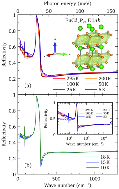
Single crystals of EuCd2P2 were grown using a flux technique that has been previously described [14]; x-ray diffraction on the large, mirror-like crystal faces revealed that they contain the a-b planes. It should be noted that there is some terracing on the surface of the crystal. The reflectivity of an as-grown crystal face () has been measured at a near-normal angle of incidence for light polarized parallel to the a-b planes over a wide temperature and frequency range ( meV to 4 eV) using an in situ evaporation technique [16]; the results are shown in Fig. 1.
The character of the reflectivity may be described as either poorly metallic, or semiconducting (insulating), depending on the temperature. The response of the reflectivity is shown in the metallic case in Fig. 1(a) at temperatures between 25 and 295 K, and at 5 K; for these temperatures the low-frequency reflectivity is increasing rapidly with decreasing frequency, which is in agreement with the requirement that when , . The two prominent features in the reflectivity that are attributed to the normally infrared-active lattice modes are also partially screened [17]. In contrast, the reflectivity in Fig. 1(b) between 10 and 18 K shows a dramatically different response; , the result expected for an insulator or semiconductor. In addition, the two lattice modes appear to be almost totally unscreened, resulting in fundamentally different line shapes [18].
The reflectivity is a combination of the real and imaginary parts of the dielectric function, and as such can be difficult to interpret; the real part of the optical conductivity, calculated from the imaginary part of the dielectric function, is a more intuitive quantity. Accordingly, the complex dielectric function, , has been determined from a Kramers-Kronig analysis of the reflectivity [19], which requires extrapolations at high and low frequency. In the case where metallic conductivity is observed, at low frequency a metallic Hagen-Rubens extrapolation, was employed, where is chosen to match the value of the reflectance at the lowest measured frequency. Where an insulating or semiconducting response is observed, below the lowest measured frequency the reflectance was assumed to be constant. Above the highest-measured frequency point the reflectance was assumed to follow a dependence up to cm-1, above which a free-electron approximation () was assumed [20]. The complex conductivity, , is calculated from from the complex dielectric function, , where high-frequency contribution to the real part of the dielectric function, and is the impedance of free space.
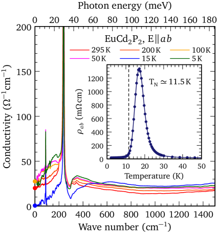
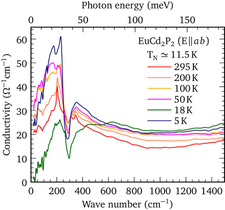
The temperature dependence of the real part of the optical conductivity for EuCd2P2 in the low-frequency region is shown in Fig. 2 for light polarized in the a-b planes. At room temperature, the optical conductivity is that of a poor metal, with , which is about a factor of two lower than the value obtained from transport [14]. Two sharp features, one weak and the other strong, are observed at about 89 and 239 cm-1, respectively. As the temperature is reduced, the low-energy conductivity increases slightly, with at 50 K, which is consistent with the decreasing resistivity observed in transport [14], shown in the inset in Fig. 2. At 10, 15 and 18 K (for clarity only the conductivity at 15 K is shown in Fig. 2), there is a dramatic decrease in the low-frequency conductivity, with a commensurate transfer of spectral weight (area under the conductivity curve) to high frequency, leading to an increase in the optical conductivity above cm-1. Interestingly, below at 5 K the metallic behavior is recovered and spectral weight is transferred back into the free-carrier component.
III Discussion
To investigate the behavior of the free-carriers in more detail, the optical response has been modeled using the Drude-Lorentz model for the complex dielectric function
| (1) |
In the first term and are the square of the plasma frequency and scattering rate for the delocalized (Drude) carriers, respectively, and and are the carrier concentration and effective mass. In the summation, , and are the position, width, and strength of a symmetric Lorentzian oscillator that describe the th vibration or bound excitation.
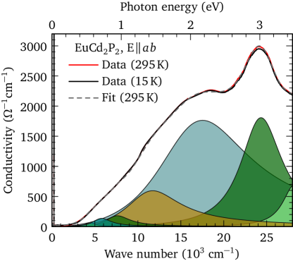
The strategy that we will adopt in fitting the optical conductivity is to first fit the interband transitions to Lorentzian oscillators using a non-linear least squares technique, then, either holding these high-frequency oscillators fixed or allowing only modest refinement, fit the free-carrier response in the low-frequency region. The general approach is to use the minimum number of oscillators required to describe the data. The real part of the in-plane optical conductivity is shown over a wide frequency range at several temperatures in Fig. 3, showing the onset of absorption above cm-1, along with the results of the fit at 295 K. Oscillators have been introduced at , 0.71, 0.95, 1.45, 2.17, 3.02, and 3.50 eV; the fit has been decomposed into the contributions from the Lorentz oscillators. While the overall fit is excellent, it can be argued that the low-frequency oscillator could probably be removed and a reasonable fit still obtained; however, the low-frequency oscillator is required to reproduce the linear region of the optical conductivity, which then allows the low-frequency conductivity to be fit reliably. We also note that because the oscillator at 3.5 eV is at the limit of the measured data, it should be treated with caution.
The determination of the frequencies for the interband transitions allows the low-frequency conductivity to be fit using the Drude model. However, the sharp features attributed to the lattice modes complicate this approach; it is simpler to fit these features and then subtract them from the conductivity, leaving only the electronic continuum associated with the free carriers. Accordingly, the rest of the discussion will first deal with the vibrational properties, followed by an analysis of the free-carrier response.
III.1 Vibrational properties
In the hexagonal (trigonal) setting, the irreducible vibrational representation for EuCd2P2 is . The and modes are Raman active, while the and modes are infrared active along the c axis and the a-b planes, respectively. The two modes observed in Fig. 2 at and 239 cm-1 are the expected modes. It is tempting to assume that the notch-like feature just above the high-frequency mode at cm-1 is due to electron-phonon coupling resulting in a Fano-like antiresonance in the electronic continuum [21, 22]. However, it should be noted that this vibration is exceptionally strong and narrow; it does not show the broadening that would be expected for a mode that was coupled to the electronic background [23]. Moreover, there is almost no electronic background for it to interact with. The low-frequency mode also displays no sign of any asymmetry. The two modes have therefore been fit using a symmetric Lorentzian on a linear background. The results of the fits to the two mode are shown in Fig.4.
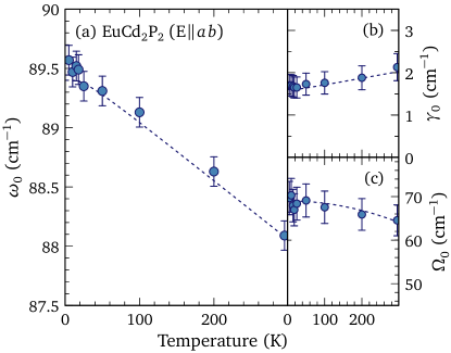
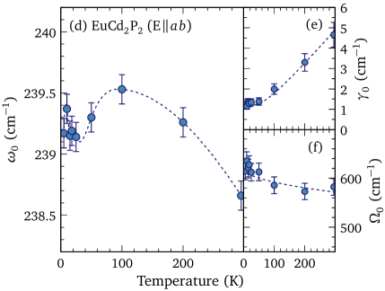
The temperature dependence of the position of the low-energy mode, shown in Fig. 4(a), behaves in the expected way, increasing in frequency (hardening) with decreasing temperature from to about 89.5 cm-1 at low temperature. At room temperature this mode is quite narrow with a line width of cm-1, and it decreases only slightly to 1.7 cm-1 at low temperature; the oscillator strength is roughly constant with cm-1. Overall, this behavior is what is expected for a symmetric anharmonic decay of an optic mode into two acoustic modes with identical frequencies and opposite momenta [24, 25]. The functional form employed here is,
| (2) |
| (3) |
where is the bare phonon frequency, is a residual line width, C and are constants, and ; the bare phonon frequency (residual line width) is recovered in the limit [26]. The model fits are indicated by the dashed lines in Figs. 4(a) and 4(b).
In contrast, the frequency dependence of the high-frequency mode, shown in Fig. 4(d), is somewhat anomalous, initially hardening with decreasing temperature, reaching a maximum of cm-1 at 100 K before softening by nearly 1 cm-1 as the temperature continues to decrease, then hardening again below about 25 K, suggesting a weak coupling to the magnetism in this material. Surprisingly, this mode narrows from to 1.3 cm-1 at low temperature in a uniform way, as shown in Fig. 4(e), and can be described by the anharmonic decay model, showing none of the anomalous behavior observed in the position, although there is some evidence the oscillator strength of this mode may increase slightly at low temperature, shown in Fig. 4(f).
The optical conductivity the fits were performed on have a typical wave number resolution of 1.8 cm-1. Measurements with a resolution of 0.2 cm-1 were performed in the far-infrared region above and below revealed that while the two modes have the same positions has previously reported, the line width of the low-frequency mode of cm-1 suggests it is limited by the resolution of the instrument, while the high-frequency mode has a width of 0.53 cm-1, indicating that this is likely its intrinsic value [18]. Interestingly, neither mode splits below , suggesting the antiferromagnetic ground state does not result in a significant lattice distortion.
III.2 Electronic response
The determination of the vibrational parameters for the two modes allows these features to be subtracted from the optical conductivity in Fig. 2, resulting in the residual conductivity shown in Fig. 5. There are several things about the residual conductivity that are unusual. The first is that the conductivity is non-Drude; it is initially increasing as a function of frequency, reaching a maximum at cm-1 before encountering a notch-like feature between cm-1. The Drude form for the real part of the optical conductivity may be written as
| (4) |
which has the form of a Lorentzian centered at zero frequency with a width of .
The origin of the notch-like feature may arise from the terraced nature of the crystal surface, which can introduce structure from the c axis into the ab-plane optical properties. Alternatively, it has been established that in anisotropic media such as the cuprate materials, measuring the reflectivity at anything other than a normal angle of incidence, or having a slightly misoriented surface, can allow c-axis longitudinal optic (LO) modes to manifest themselves as antiresonaces (resonances) in the metallic (insulating) electronic background [27, 28, 29]. The results from an a-c [(101)] face allows the positions of the transverse optic (TO) modes to be determined and the lower bound of the LO modes to be estimated; comparison with the in-plane results reveal that the artifacts in the a-b plane reflectivity arise from the c axis TO modes. The terraces lead to a mixing of the in-plane and c axis reflectivity, thus the notch-like feature is considered to be an artifact and not intrinsic and will be ignored in fits to the residual conductivity; this is discussed in detail in the Supplementary Materials [18].
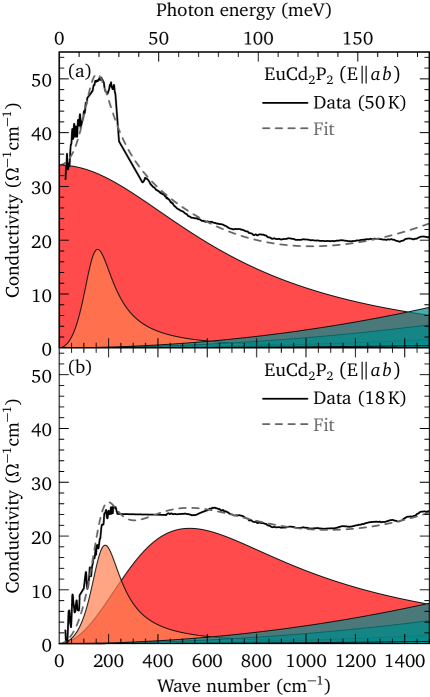
The residual optical conductivity has been fit using the Drude-Lorentz model and the results for two representative fits at 50 and 18 K are shown in Figs. 6(a) and 6(b), respectively; the bound excitations associated with the interband transitions have been held fixed, partly to allow for a more reliable convergence, and also because little temperature dependence of these features is expected (Fig. 3). The quality of the fits are quite good. In the metallic state at 50 K, the Drude response dominates the free-carrier response with cm-1 with a scattering rate of cm-1, values that are representative of a marginally-metallic material. A weak bound excitation at cm-1 has been included to reproduce the non-Drude response at low frequency; however, it represents only about 10% of the spectral weight associated with the free carriers. At 18 K, the Drude response vanishes and essentially all of the spectral weight associated with free carriers has been transferred to a bound excitation at cm-1, with a width cm-1 and cm-1. The results of the fits have been summarized in Table 1. While position of the excitation at cm-1 shows little temperature dependence, it does increase somewhat in strength below , suggesting that it is affected by the formation of magnetic order; however, its origin remains unclear.
| 295 | 993 | 756 | |||
| 200 | 1100 | 753 | |||
| 100 | 1160 | 680 | |||
| 50 | 1193 | 698 | |||
| 25 | 1311 | 1265 | |||
| 18 | 486 | 1180 | 1183 | ||
| 15 | 539 | 1028 | 1154 | ||
| 10 | 426 | 770 | 1078 | ||
| 5 | 1170 | 919 |
The temperature dependence of Drude plasma frequency is roughly constant with a value of cm-1. When the Drude term vanishes at temperatures close to the resistivity maximum, the free-carrier spectral weight is transferred into a localized excitation with , which is also temperature independent. On the other hand, the Drude scattering rate decreases from to 700 cm-1 at 50 K, but then increases dramatically at 25 K, just above the resistivity maximum, to cm-1. It is tempting to associate the rapid increase in close to with the scattering of carriers from antiferromagnetic fluctuations. This argument would be reasonable if the maximum in the resistivity occurred just above ; however, it occurs at K, nearly twice . Moreover, the resistivity in this material increases by roughly two orders of magnitude, far greater than the modest increases that are observed at in the As and Sb compounds.
A more conventional approach relies on polaron effects to describe the transport behavior in the colossal magnetoresistance materials [30, 31, 32, 33, 34, 35]. For instance, a transition from large (delocalized carriers) to small polarons (localized carriers) has been used to explain the metal-insulator transition in manganites [36, 37]. The application of polarons to this material is attractive because the shape of the electronic absorption is that of an asymmetric Gaussian with a long high-frequency tail [37], which it could be argued better describes the electronic background in Fig. 6(b) than the two Lorentzian oscillators; additionally, the peak of the localized carriers occurs at cm-1, which is roughly twice the energy of the high-frequency mode, consistent with a polaronic mechanism. There is are several problems with this interpretation. The first is that small lattice polarons are expected to form in systems with strong electron-phonon coupling [35]; however, as previously noted, the narrow line shapes of the infrared-active modes do not support the notion of strong electron-phonon coupling. Additionally, the size of this effect is orders of magnitude smaller than what is observed in the manganites, and finally, no removal of degeneracy due to the coupling of the infrared-active modes to a lattice distortion is observed. Consequently, the polaronic view is not favored.
The most compelling explanation for the dramatic increase of the resistivity above lies in the recent observation of the formation of ferromagnetism at [1]; ferromagnetic clusters form in a paramagnetic background, resulting in carriers becoming localized into spin-polarized clusters due to spin-carrier coupling. Optically, this is observed as the transfer of spectral weight from the free-carriers into a localization peak. The resistivity continues to increase until the ferromagnetic regions begin to merge into a contiguous network just above , at which point the resistivity begins to decrease and the spectral weight is transferred back into the free-carrier component. The ferromagnetic regions are observed to persist below in the metallic antiferromagnetic phase where the conductivity has improved slightly, likely due to a decrease in spin fluctuations [38].
IV Conclusions
The optical properties of a single crystal of EuCd2P2 have been determined for light polarized in the a-b planes above and below over a wide frequency range. At room temperature, the real part of the optical conductivity reveals a marginally-metallic material, consisting of a weak free-carrier component with the onset of interband transitions above cm-1. Two sharp infrared-active modes are observed at and 239 cm-1. In addition, a spurious notch-like feature observed in the in-plane conductivity is attributed to c-axis contamination due to terraces in the crystal surface [18]. As the temperature is lowered, there is a modest increase in the low-frequency conductivity; however, below about 50 K the conductivity begins to decrease until at K (just below ), a dramatic change is observed as the majority of the free-carriers enter into a localized state, before reverting back to metallic behavior again below . The loss and subsequent restoration of the free-carrier electronic background has a relatively minor effect on the nature of the modes; however, it results in a dramatic change in the line shapes of these vibrations in the reflectivity [18]. The localization of the free carriers is intimately connected with the magnetism in this material. While several scenarios are considered, the prevailing explanation for the resistivity maximum and carrier localization is the formation of ferromagnetic domains below that result in spin-polarized clusters due to spin-carrier coupling; once these domains form a contiguous network, the resistivity decreases and the free-carrier component is restored [1].
Acknowledgements.
We would like to acknowledge useful discussions with A. Akrap, V. Sunko and J. Orenstein. The work at Boston College was funded by the National Science Foundation under Award No. NSF/DMR-1708929. Work at Brookhaven National Laboratory was supported by the Office of Science, U.S. Department of Energy under Contract No. DE-SC0012704.References
- Sunko et al. [2022] V. Sunko, Y. S. M. Vranas, C. C. Homes, C. Lee, E. Donoway, Z.-C. Wang, S. Balguri, M. B. Mahendru, A. Ruiz, B. Gunn, R. Basak, E. Schierle, E. Weschke, F. Tafti, A. Frano, and J. Orenstein, Spin-carrier coupling induced ferromagnetism and giant resistivity peak in EuCd2P2, arXiv:2208.05499v1 (2022).
- Wang et al. [2016] H. P. Wang, D. S. Wu, Y. G. Shi, and N. L. Wang, Anisotropic transport and optical spectroscopy study on antiferromagnetic triangular lattice EuCd2As2: An interplay between magnetism and charge transport properties, Phys. Rev. B 94, 045112 (2016).
- Ma et al. [2019] J.-Z. Ma, S. M. Nie, C. J. Yi, J. Jandke, T. Shang, M. Y. Yao, M. Naamneh, L. Q. Yan, Y. Sun, A. Chikina, V. N. Strocov, M. Medarde, M. Song, Y.-M. Xiong, G. Xu, W. Wulfhekel, J. Mesot, M. Reticcioli, C. Franchini, C. Mudry, M. Müller, Y. G. Shi, T. Qian, H. Ding, and M. Shi, Spin fluctuation induced Weyl semimetal state in the paramagnetic phase of EuCd2As2, Sci. Adv. 5, eaaw4718 (2019).
- Wang et al. [2019] L.-L. Wang, N. H. Jo, B. Kuthanazhi, Y. Wu, R. J. McQueeney, A. Kaminski, and P. C. Canfield, Single pair of Weyl fermions in the half-metallic semimetal EuCd2As2, Phys. Rev. B 99, 245147 (2019).
- Behrends et al. [2019] J. Behrends, R. Ilan, and J. H. Bardarson, Anomalous conductance scaling in strained Weyl semimetals, Phys. Rev. Research 1, 032028 (2019).
- Soh et al. [2019] J.-R. Soh, F. de Juan, M. G. Vergniory, N. B. M. Schröter, M. C. Rahn, D. Y. Yan, J. Jiang, M. Bristow, P. Reiss, J. N. Blandy, Y. F. Guo, Y. G. Shi, T. K. Kim, A. McCollam, S. H. Simon, Y. Chen, A. I. Coldea, and A. T. Boothroyd, Ideal Weyl semimetal induced by magnetic exchange, Phys. Rev. B 100, 201102 (2019).
- Jo et al. [2020] N. H. Jo, B. Kuthanazhi, Y. Wu, E. Timmons, T.-H. Kim, L. Zhou, L.-L. Wang, B. G. Ueland, A. Palasyuk, D. H. Ryan, R. J. McQueeney, K. Lee, B. Schrunk, A. A. Burkov, R. Prozorov, S. L. Bud’ko, A. Kaminski, and P. C. Canfield, Manipulating magnetism in the topological semimetal EuCd2As2, Phys. Rev. B 101, 140402(R) (2020).
- Su et al. [2020] H. Su, B. Gong, W. Shi, H. Yang, H. Wang, W. Xia, Z. Yu, P.-J. Guo, J. Wang, L. Ding, L. Xu, X. Li, X. Wang, Z. Zou, N. Yu, Z. Zhu, Y. Chen, Z. Liu, K. Liu, G. Li, and Y. Guo, Magnetic exchange induced Weyl state in a semimetal EuCd2Sb2, APL Materials 8, 011109 (2020).
- Ma et al. [2020] J. Ma, H. Wang, S. Nie, C. Yi, Y. Xu, H. Li, J. Jandke, W. Wulfhekel, Y. Huang, D. West, P. Richard, A. Chikina, V. N. Strocov, J. Mesot, H. Weng, S. Zhang, Y. Shi, T. Qian, M. Shi, and H. Ding, Emergence of Nontrivial Low-Energy Dirac Fermions in Antiferromagnetic EuCd2As2, Adv. Mater. 32, 1907565 (2020).
- Xu et al. [2021] Y. Xu, L. Das, J. Z. Ma, C. J. Yi, S. M. Nie, Y. G. Shi, A. Tiwari, S. S. Tsirkin, T. Neupert, M. Medarde, M. Shi, J. Chang, and T. Shang, Unconventional Transverse Transport above and below the Magnetic Transition Temperature in Weyl Semimetal EuCd2As2, Phys. Rev. Lett. 126, 076602 (2021).
- Schellenberg et al. [2011] I. Schellenberg, U. Pfannenschmidt, M. Eul, C. Schwickert, and R. Pöttgen, A 121Sb and 151Eu Mössbauer Spectroscopic Investigation of EuCd ( = P, As, Sb) and YbCd2Sb2, Z. Anorg. Allg. Chem. 637, 1863 (2011).
- Rahn et al. [2018] M. C. Rahn, J.-R. Soh, S. Francoual, L. S. I. Veiga, J. Strempfer, J. Mardegan, D. Y. Yan, Y. F. Guo, Y. G. Shi, and A. T. Boothroyd, Coupling of magnetic order and charge transport in the candidate Dirac semimetal EuCd2As2, Phys. Rev. B 97, 214422 (2018).
- Soh et al. [2020] J.-R. Soh, E. Schierle, D. Y. Yan, H. Su, D. Prabhakaran, E. Weschke, Y. F. Guo, Y. G. Shi, and A. T. Boothroyd, Resonant x-ray scattering study of diffuse magnetic scattering from the topological semimetals EuCd2As2 and EuCd2Sb2, Phys. Rev. B 102, 014408 (2020).
- Wang et al. [2021] Z.-C. Wang, J. D. Rogers, X. Yao, R. Nichols, K. Atay, B. Xu, J. Franklin, I. Sochnikov, P. J. Ryan, D. Haskel, and F. Tafti, Colossal magnetoresistance without mixed valence in a layered phosphide crystal, Adv. Mater. 33, 2005755 (2021).
- Momma and Izumi [2011] K. Momma and F. Izumi, VESTA 3 for three-dimensional visualization of crystal, volumetric and morphology data, J. Appl. Crystr. 44, 1272 (2011).
- Homes et al. [1993] C. C. Homes, M. Reedyk, D. A. Crandles, and T. Timusk, Technique for measuring the reflectance of irregular, submillimeter-sized samples, Appl. Opt. 32, 2976 (1993).
- Homes et al. [2000] C. C. Homes, A. W. McConnell, B. P. Clayman, D. A. Bonn, R. Liang, W. N. Hardy, M. Inoue, H. Negishi, P. Fournier, and R. L. Greene, Phonon Screening in High-Temperature Superconductors, Phys. Rev. Lett. 84, 5391 (2000).
- [18] See Supplemental Material at [URL will be inserted by publisher] for a discussion of how a weak electronic background can fundamentally alter the vibrational line shape in the reflectivity. Examples of terracing in EuCd2P2 are shown; the experimental high-resolution (0.2 cm-1) in-plane [(001)] reflectivty, as well as the reflectivity from an a-c [(101)] face is shown. The fitted values of the in-plane and c-axis modes, as well as estimates for the positions of the LO modes, are presented; estimates of are validated by examining the positions of the a-b plane TO and LO modes. The analysis concludes that terracing leads to artifacts in the reflectivity due to the simple mixing of the a-b plane and c axis reflectivity.
- Dressel and Grüner [2001] M. Dressel and G. Grüner, Electrodynamics of Solids (Cambridge University Press, Cambridge, 2001).
- Wooten [1972] F. Wooten, Optical Properties of Solids (Academic Press, New York, 1972) pp. 244–250.
- Fano [1961] U. Fano, Effects of configuration interaction on intensities and phase shifts, Phys. Rev. 124, 1866 (1961).
- Damascelli [1996] A. Damascelli, Optical Spectroscopy of Quantum Spin Systems, Ph.D. thesis, University of Groningen (1996), p. 21.
- Wang et al. [2017] Y. Wang, L. Rademaker, E. Dagotto, and S. Johnston, Phonon linewidth due to electron-phonon interactions with strong forward scattering in FeSe thin films on oxide substrates, Phys. Rev. B 96, 054515 (2017).
- Klemens [1966] P. G. Klemens, Anharmonic decay of optical phonons, Phys. Rev. 148, 845 (1966).
- Menéndez and Cardona [1984] J. Menéndez and M. Cardona, Temperature dependence of the first-order Raman scattering by phonons in Si, Ge, and : Anharmonic effects, Phys. Rev. B 29, 2051 (1984).
- Homes et al. [2016] C. C. Homes, Y. M. Dai, J. Schneeloch, R. D. Zhong, and G. D. Gu, Phonon anomalies in some iron telluride materials, Phys. Rev. B 93, 125135 (2016).
- Berreman [1970] D. W. Berreman, Resonant Reflectance Anomalies: Effect of Shapes of Surface Irregularities, Phys. Rev. B 1, 381 (1970).
- Reedyk and Timusk [1992] M. Reedyk and T. Timusk, Evidence for a-b-plane coupling to longitudinal c-axis phonons in high- superconductors, Phys. Rev. Lett. 69, 2705 (1992).
- Homes et al. [2007] C. C. Homes, J. M. Tranquada, and D. J. Buttrey, Stripe order and vibrational properties of La2NiO4+δ for : Measurements and ab initio calculations, Phys. Rev. B 75, 045128 (2007).
- Emin [1993] D. Emin, Optical properties of large and small polarons and bipolarons, Phys. Rev. B 48, 13691 (1993).
- Alexandrov and Mott [1995] A. S. Alexandrov and N. Mott, Polarons & Bipolarons (World Scientific, Cambridge, 1995).
- Millis et al. [1996] A. J. Millis, R. Mueller, and B. I. Shraiman, Fermi-liquid-to-polaron crossover. II. Double exchange and the physics of colossal magnetoresistance, Phys. Rev. B 54, 5405 (1996).
- Röder et al. [1996] H. Röder, J. Zang, and A. R. Bishop, Lattice Effects in the Colossal-Magnetoresistance Manganites, Phys. Rev. Lett. 76, 1356 (1996).
- Lee and Min [1997] J. D. Lee and B. I. Min, Polaron transport and lattice dynamics in colossal-magnetoresistance manganites, Phys. Rev. B 55, 12454 (1997).
- Salamon and Jaime [2001] M. B. Salamon and M. Jaime, The physics of manganites: Structure and transport, Rev. Mod. Phys. 73, 583 (2001).
- Lanzara et al. [1998] A. Lanzara, N. L. Saini, M. Brunelli, F. Natali, A. Bianconi, P. G. Radaelli, and S.-W. Cheong, Crossover from Large to Small Polarons across the Metal-Insulator Transition in Manganites, Phys. Rev. Lett. 81, 878 (1998).
- Hartinger et al. [2004] C. Hartinger, F. Mayr, J. Deisenhofer, A. Loidl, and T. Kopp, Large and small polaron excitations in La2/3(Sr/Ca)1/3MnO3 films, Phys. Rev. B 69, 100403(R) (2004).
- Zhang et al. [2010] Y. Zhang, F. Chen, C. He, L. X. Yang, B. P. Xie, Y. L. Xie, X. H. Chen, M. Fang, M. Arita, K. Shimada, H. Namatame, M. Taniguchi, J. P. Hu, and D. L. Feng, Strong correlations and spin-density-wave phase induced by a massive spectral weight redistribution in Fe1.06Te, Phys. Rev. B 82, 165113 (2010).
![[Uncaptioned image]](/html/2209.10606/assets/x8.png)
![[Uncaptioned image]](/html/2209.10606/assets/x9.png)
![[Uncaptioned image]](/html/2209.10606/assets/x10.png)
![[Uncaptioned image]](/html/2209.10606/assets/x11.png)
![[Uncaptioned image]](/html/2209.10606/assets/x12.png)