HiRA: Hidden Row Activation
for Reducing Refresh Latency of Off-the-Shelf DRAM Chips
Abstract
DRAM is the building block of modern main memory systems. DRAM cells must be periodically refreshed to prevent data loss. Refresh operations degrade system performance by interfering with memory accesses. As DRAM chip density increases with technology node scaling, refresh operations also increase because: 1) the number of DRAM rows in a chip increases; and 2) DRAM cells need additional refresh operations to mitigate bit failures caused by RowHammer, a failure mechanism that becomes worse with technology node scaling. Thus, it is critical to enable refresh operations at low performance overhead. To this end, we propose a new operation, Hidden Row Activation (HiRA), and the HiRA Memory Controller (HiRA-MC) to perform HiRA operations.
HiRA hides a refresh operation’s latency by refreshing a row concurrently with accessing or refreshing another row within the same bank. Unlike prior works, HiRA achieves this parallelism without any modifications to off-the-shelf DRAM chips. To do so, it leverages the new observation that two rows in the same bank can be activated without data loss if the rows are connected to different charge restoration circuitry. We experimentally demonstrate on real off-the-shelf DRAM chips that HiRAcan reliably parallelize a DRAM row’s refresh operation with refresh or activation of any of the of the rows within the same bank. By doing so, HiRA reduces the overall latency of two refresh operations by .
HiRA-MC modifies the memory request scheduler to perform HiRA when a refresh operation can be performed concurrently with a memory access or another refresh. Our system-level evaluations show that HiRA-MC increases system performance by and as it reduces the performance degradation due to periodic refreshes and refreshes for RowHammer protection (preventive refreshes), respectively, for future DRAM chips with increased density and RowHammer vulnerability.
1 Introduction
DRAM [28] is the prevalent main memory technology used in a wide variety of computing systems from cloud servers to mobile devices due to its high density and low latency. A DRAM cell encodes a bit of data as electrical charge, which inherently leaks over time [70]. Therefore, to ensure reliable operation and data integrity, a DRAM cell needs to be periodically refreshed [55, 60, 61, 57, 58, 59]. Unfortunately, these refresh operations degrade system performance by interfering with memory accesses [103, 20]. During a refresh operation, which is performed at row granularity (e.g., 8KB), the memory cannot service any requests to the DRAM bank (e.g., 512MB) or rank (e.g., 8GB) that contains the refreshed row [113, 60, 57].
As DRAM density increases with technology node scaling, the performance overhead of refresh also increases due to three major reasons. First, as the DRAM chip density increases, more DRAM rows need to be periodically refreshed in a DRAM chip [55, 60, 61, 57, 58, 59]. Second, as DRAM technology node scales down, DRAM cells become smaller and thus can store less amount of charge, requiring them to be refreshed more frequently [124, 103, 10, 102, 20, 67, 118, 122, 123]. Third, with increasing DRAM density, DRAM cells are placed closer to each other, exacerbating charge leakage via a disturbance error mechanism called RowHammer [84, 79, 119, 183, 120, 167, 133, 134, 180], and thus requiring additional refresh operations (called preventive refreshes) to avoid data corruption due to RowHammer [2, 84, 76, 5, 3, 7, 6, 157, 152, 185, 97, 135, 179, 33, 66, 42, 141, 82, 29, 98, 107, 189, 63]. Prior work shows that 1) RowHammer can be exploited to escalate privilege, leak private data, and manipulate critical application outputs [149, 164, 38, 142, 138, 174, 13, 11, 139, 53, 1, 119, 162, 37, 101, 165, 32, 25, 62, 120, 45, 92, 33, 24, 171, 188, 145, 184, 27, 42, 54, 163, 15, 14, 84, 88]; and 2) modern DRAM chips, including the ones that are marketed as RowHammer-safe [33, 99, 113], are more vulnerable to RowHammer than their predecessors [84, 119, 120, 79, 33, 42, 129, 54, 180, 27]. Therefore, defending against RowHammer is critical for secure system operation and doing so likely requires aggressively refreshing the cells disturbed by RowHammer [79, 42, 129, 179, 181, 135, 141]. As a result of these three major reasons, newer generations of DRAM chips require performing more refresh operations compared to their predecessors. Thus, it is critical to reduce the performance overhead of refreshes.
Prior works suggest reducing refresh latency by 1) accelerating the charge restoration process [105, 40] and 2) exploiting parallelism across subarrays within a DRAM bank [85, 20, 169, 186]. Unfortunately, these proposals require modifications to DRAM circuitry, making them unsuitable for already deployed off-the-shelf DRAM chips. Therefore, it is important to find alternative solutions to reduce the negative performance impact of a refresh operation with no modifications to the DRAM chip circuitry.
Our goal is to reduce the refresh latency in off-the-shelf DRAM chips with no modifications to DRAM circuitry. To this end, we propose a new operation called Hidden Row Activation (HiRA)and the HiRA Memory Controller (HiRA-MC) to perform HiRA operations.
HiRA enables refreshing a DRAM row while refreshing or accessing another DRAM row within the same bank. HiRA leverages the new observation that opening two rows, whose charge restoration circuitries are electrically isolated from each other, in rapid succession, allows refreshing one row while refreshing or accessing the other row. To open two such rows in rapid succession, HiRAuses a carefully-engineered sequence of activate () and precharge () commands, already implemented in off-the-shelf DRAM chips for opening and closing DRAM rows, respectively. We experimentally demonstrate on real off-the-shelf DRAM chips that HiRA 1) reliably parallelizes a DRAM row’s refresh operation with refresh or activation of any of the of the rows within the same bank and 2) effectively reduces the overall latency of refreshing two rows by .
The HiRA Memory Controller (HiRA-MC) leverages the HiRAoperation to improve system performance by performing two main tasks. First, it queues each refresh request with a time slack before the refresh needs to be performed and assigns the refresh request a deadline. Second, it observes the memory accesses at real-time to find a memory access that can be performed concurrently with a queued refresh request. HiRA-MC ensures that each periodic and preventive refresh request is performed by its deadline. HiRA-MC achieves this by taking one of three possible actions, in the following order: 1) refresh a DRAM row concurrently with a memory access (refresh-access parallelization) before the refresh operation’s deadline; 2) refresh a row concurrently with another refresh operation (refresh-refresh parallelization) if refresh-access parallelization is not possible until the refresh operation’s deadline; or 3) perform a refresh operation right at its deadline if neither refresh-access nor refresh-refresh parallelization is possible. We evaluate HiRA-MC’s hardware complexity and show that it consumes only chip area and responds to queries within (in parallel to a command with a latency of ). To evaluate HiRA-MC’s performance benefits, we conduct cycle-level simulations on 125 multiprogrammed workloads. Our analysis shows that 1) without HiRA, periodic and preventive refresh operations cause and performance overhead for future DRAM chips with high density and high RowHammer vulnerability, respectively, compared to an ideal memory controller that does not perform periodic or preventive refreshes and 2) HiRA-MCincreases system performance by and as it reduces the performance degradation due to periodic refreshes and preventive refreshes, respectively, for future DRAM chips with increased density and RowHammer vulnerability.
This paper makes the following contributions:
-
This is the first work to show that refresh-refresh and refresh-access parallelization within a bank is possible in off-the-shelf DRAM chips by issuing a carefull-engineered sequence of activate () and precharge ()commands, which we call Hidden Row Activation (HiRA).
-
We experimentally demonstrate on real DDR4 DRAM chips that HiRA 1) reduces the latency of refreshing two rows back-to-back by , and 2) reliably parallelizes a DRAM row’s refresh operation with refresh or activation of any of the of the rows in the same bank.
-
We design the HiRA Memory Controller (HiRA-MC) to perform HiRA operations. We show that HiRA-MC significantly improves system performance by and as it reduces the performance degradation due to periodic refreshes and preventive refreshes for RowHammer, respectively.
2 Background
This section describes the background required to understand the rest of the paper. For a more comprehensive description of DRAM organization and operation, we refer the reader to [85, 103, 95, 70, 96].
2.1 DRAM Organization
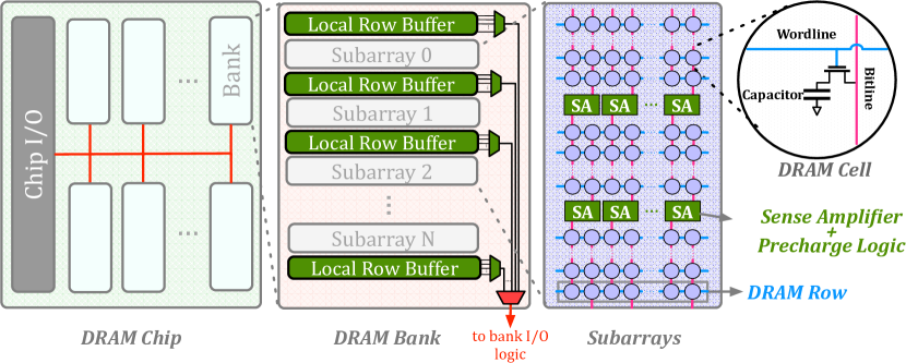
DRAM is organized hierarchically. The memory controller accesses DRAM modules via a memory channel. A DRAM module has one or more ranks, each of which contains multiple DRAM chips that work in lock-step. Each DRAM chip consists of multiple DRAM banks, which share the I/O circuitry of the chip (called chip I/O).
Bank Organization. Fig. 1 shows a typical DRAM chip organization, containing multiple banks. A DRAM bank is composed of multiple subarrays, which share the I/O circuitry of the bank (called bank I/O). Each subarray contains a two-dimensional array of DRAM cells, organized as rows and columns and a local row buffer. A DRAM cell stores data as electrical charge in a capacitor, which is accessed via an access transistor. The gate of an access transistor is driven by a row-wide wire, called wordline. The access transistor connects the cell capacitor to a column-wide structure, called bitline. A bitline is connected to a sense amplifier (SA) and precharge circuitry.
Open-bitline Architecture. To optimize the size and layout of subarrays, the common open-bitline architecture [21, 71, 105] places the SAs on both ends (i.e., top and bottom) of the subarray (as depicted in Fig. 1). In this architecture, horizontally adjacent DRAM cells are connected via bitlines to SAs on both ends of the subarray.
2.2 DRAM Operation
The memory controller implements a memory request scheduler to issue DDRx commands. We describe the four DDRx commands that are relevant to this work.
Precharge. A bitline needs to be precharged to half of the supply voltage () before accessing a DRAM row in a subarray. To do so, the precharge () command prepares the subarray for accessing data in DRAM cells using the precharge logic placed next to the sense amplifiers.
Row Activation. To access a DRAM cell, the memory controller needs to open the DRAM row containing the cell. To do so, the memory controller issues an activate () command. An command is performed in four steps. First, it drives the target wordline with a high voltage level to turn on the access transistors within the DRAM row (i.e., open the DRAM row). Second, turning on an access transistor initiates the charge sharing process between the DRAM cell and its bitline. Third, the charge sharing process causes a small deviation in the bitline voltage. Fourth, the sense amplifier is enabled to sense the voltage deviation on the bitline and amplify the bitline voltage to the level of either the supply voltage () or ground () (depending on the voltage deviation on the bitline). In doing so, an command copies the data in the open DRAM row to the local row buffer.
Column Access. Once the open row is copied to the local row buffer, it can be accessed by read () or modified by write () column access commands in the local row buffer using the bank I/O circuitry. Only one DRAM row in a bank can be open at a given time [60, 85].
Timing Parameters. DRAM specifications (e.g., DDR4 [60]) define timing parameters that the memory controller obeys while scheduling DRAM commands. Four timing parameters are important to understand the rest of the paper. First, consecutive row activation and column access commands (e.g., to ) must be separated in time by at least the row-to-column delay or row activation latency (). ensures that the deviation in the bitline voltage exceeds the reliable sensing threshold of the sense amplifier during row activation [78, 19]. Second, consecutive and commands must be separated by at least the charge restoration latency (). ensures that the charge levels of all DRAM cells in the open row are fully restored before the row is closed. Third, consecutive precharge and row activation commands must be separated by at least the precharge latency (). ensures that the bitline is fully precharged to , so that the next row activation can be reliably performed. Fourth, the time window between two consecutive row activations targeting a DRAM bank, i.e., row activation cycle ()must be at least as large as the sum of and .
2.3 DRAM Refresh
Charge stored in the capacitor of a DRAM cell leaks over time. Therefore, the charge in the cell’s capacitor must be periodically restored (i.e., the DRAM cell must be refreshed) to maintain data integrity. The time interval during which a cell can retain its charge without being refreshed is called the cell’s retention time. A DRAM cell needs to be refreshed once every refresh window (), which is typically (e.g., in DDR4 [60]) or (e.g., in DDR5 [61]).
To perform refresh operations, the memory controller periodically issues a refresh () command to a DRAM rank after every refresh interval () (e.g., [60] or [61]). Each command refreshes a number of rows in the DRAM chip based on the chip’s capacity. The DRAM chip internally decides which rows and how many rows to refresh, but does not expose this information to the memory controller.
Issuing a command makes the DRAM rank unavailable for a time window called refresh latency (), during which the rank cannot receive any commands. Unfortunately, needs to be large enough (e.g., [60]) such that multiple rows can be refreshed with a command. Thus, issuing a command can increase the access latency of memory requests and cause system-wide slowdown. With increasing DRAM chip density, more DRAM rows need to be refreshed, exacerbating the negative performance impact of DRAM refresh [124, 103].
2.4 RowHammer
Modern DRAM devices suffer from disturbance errors that happen when a DRAM row (the aggressor row) is repeatedly and rapidly activated [84, 119, 120]. These disturbance errors manifest in DRAM rows neighboring the aggressor row (i.e., victim rows) after the aggressor row’s activation count (i.e., hammer count) reaches a certain threshold value within a refresh window, which we call the RowHammer threshold () [79, 84, 129, 180]. As DRAM cells become smaller and closer to each other with technology node scaling, RowHammer vulnerability becomes worse [84, 119, 120, 79, 33, 42, 129, 54, 180, 27]. Given the severity of the RowHammer vulnerability, many prior works propose refreshing the potential victim rows to prevent RowHammer bit flips, which we call preventive refresh [2, 84, 76, 5, 3, 7, 6, 157, 152, 185, 97, 135, 179, 33, 66, 42, 141, 82, 29, 98, 107, 189, 63].
3 HiRA: Hidden Row Activation
Overview. We develop the Hidden Row Activation (HiRA) operation for concurrently activating two DRAM rows within a DRAM bank. HiRA overlaps the latency of refreshing a DRAM row with the latency of refreshing or activating another DRAM row in the same DRAM bank. Fig. 2 demonstrates how a HiRAoperation is performed by issuing a carefully-engineered sequence of , , and commands with two customized timing parameters: ( to latency) and ( to latency). A HiRA operation’s first refreshes and the second refreshes and opens it for column accesses. Since and commands are already implemented in off-the-shelf DRAM chips, HiRA does not require modifications to the DRAM chip circuitry.
At a high level, a HiRA operation 1) activates , 2) precharges the bank without disconnecting from its local row buffer, and 3) activates . In doing so, it allows the memory controller to 1) perform two refresh operations on and with a latency significantly smaller than two times the (i.e., refresh-refresh parallelization) and 2) activate for column accesses (i.e., only ’s local row buffer gets connected to the bank I/O after performing a HiRA operation) concurrently with refreshing (i.e., refresh-access parallelization).
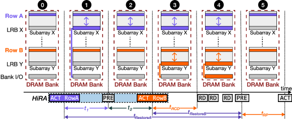
HiRA Operation Walk-Through. Fig. 2 demonstrates how a HiRA operation is performed and how it affects the state of a DRAM bank. Initially ( ) the DRAM bank is in precharged state and thus there is no active row. HiRA begins by issuing an command targeting , which connects ’s cells to local row buffer X ( ). Then, a precharge command is issued to disconnect local row buffer (LRB) X from the bank I/O ( ). This precharge operation is interrupted by issuing a new row activation, targeting in a completely separate subarray Y ( ), to avoid breaking the connection between the local row buffer X and . Therefore, the sense amplifiers in the local row buffer X continue charge restoration of . Thus, HiRA overlaps the latency of refreshing with the latency of activating . It is important that the subarray that contains (subarray Y) is physically isolated from the subarray that contains (subarray X), such that subarrays X and Y do not share any bitline or sense amplifier and thus activating does not affect the voltage levels on subarray X’s bitlines ( ). The HiRA operation completes when the second row activation is issued, after which both and are connected to their local row buffers without corrupting each other’s data ( ). Following a HiRA operation, ’s content can be read by issuing commands once is satisfied ( ). To close both and , issuing one precharge command is enough ( ).111Our experiments verify that issuing one precharge command is enough to reliably close both rows in all real DRAM chips we test. We hypothesize that issuing a command disables all wordlines and precharges all bitlines in a DRAM bank because the precharge command is not provided with a row address [55, 59, 60, 57, 58, 61, 113].
Charge Restoration after HiRA. Fig. 2 highlights the charge restoration time that and experience as and , respectively. To ensure charge restoration happens correctly for and , both and should be larger than or equal to the existing timing parameter [55, 59, 60, 57, 58, 61, 113]. Because we do not modify the timing constraints of the second command ( ), existing DRAM timing restrictions already ensure that is larger than or equal to the nominal . Since is already larger than (because is activated earlier than ), we conclude that charge restoration happens correctly for both rows.
HiRA’s Novelty. HiRA’s command sequence (--) is similar to the command sequences used in multiple prior works [34, 127, 126]. These prior works use the -- command sequence to activate two rows in the same subarray for various purposes (which we explain below). In contrast, HiRA’s purpose is to activate two rows in different subarrays such that we can refresh a DRAM row concurrently with refreshing or activating another row in the same bank.
First, ComputeDRAM [34] and PiDRAM [126] perform an -- command sequence to enable bulk data copy across DRAM rows in the same subarray (also known as RowClone [150]) in off-the-shelf DRAM chips. Second, QUAC-TRNG [127] uses -- command sequence for performing an operation called quadruple row activation, which concurrently activates four rows whose addresses vary only in the least significant two bits. 1) The RowClone [150] implementations of both ComputeDRAM [34] and PiDRAM [126] and 2) QUAC-TRNG’s [127] quadruple row activation require using two rows within the same subarray, so that the bitlines and local sense amplifiers are used for sharing the electrical charge across activated DRAM rows. Therefore, these works do not activate DRAM rows in different subarrays. In contrast, HiRA exclusively targets two rows in different subarrays, so that it enables the memory controller to perform two key operations that were not known to be possible before on off-the-shelf DRAM chips: 1) concurrently refreshing two rows, and 2) refreshing one row while activating another row in a different subarray.
HiRA’s Main Benefit. HiRA largely overlaps a DRAM row’s charge restoration latency ( in Fig. 2) with the latency of another row’s activation and charge restoration ( and in Fig. 2, respectively). Doing so allows HiRA to reduce the latency of two operations. First, HiRA reduces the latency of a memory access request that is scheduled immediately after a refresh operation. With HiRA, such a request experiences a latency of ( and in Fig. 2), which can be as small as (§4.2), instead of the nominal row cycle time of ( [60, 113]). Second, HiRA reduces the overall latency of refreshing two DRAM rows in the same bank. With HiRA, such an operation takes only ( for the HiRA operation to complete (§4.2) and to ensure that is large enough to complete charge restoration [60, 113]) instead of the nominal latency of .222To refresh two rows using nominal timing parameters, a conventional memory controller 1) activates the first row and waits until charge restoration is complete (), 2) precharges the bank and waits until all bitlines are ready for the next row activation (), and 3) activates the second row and waits until charge restoration is complete () [60, 113].
HiRA Operating Conditions. A HiRA operation works reliably if four conditions are satisfied. First, should be large enough so that the sense amplifiers are enabled before the precharge command is issued ( in Fig. 2). Second, should be small enough so that the second activate command ( in Fig. 2) interrupts the precharge operation before ’s wordline is disabled, allowing charge restoration on to complete correctly. Third, should be large enough to disconnect the local row buffer X from the bank I/O logic if HiRA is performed for refresh-access parallelization, so that future column accesses are performed only on (LRB Y). This constraint does not apply to refresh-refresh parallelization because the bank I/O logic is not used during refresh. Fourth, and should be located in two different subarrays that are physically isolated from each other, such that they do not share any sense amplifier or bitline.
4 HiRA in Off-the-Shelf DRAM Chips
In this section, we demonstrate that HiRA works reliably on real DDR4 DRAM chips. Table 1 provides the chip density, die revision (Die Rev.), chip organization (Org.), and manufacturing date of tested DRAM modules where DRAM chips are manufactured by SK Hynix.333We observe that HiRA reliably works only in DRAM chips from SK Hynix (similar to QUAC-TRNG [127]) out of 40, 40, and 56 DRAM chips that we test from three major DRAM manufacturers: Micron, Samsung, and SK Hynix, respectively. §12 discusses why we do not observe a successful HiRA operation in DRAM chips manufactured by Micron and Samsung. A is F4-2400C17S-8GNT from GSKill [39], B is KSM32RD8/16HDR from Kingston [87], and C is HMAA4GU6AJR8N-XN from SK Hynix [109]. We report the manufacturing date of these modules in the form of .
| Model |
|
|
|
|
|
|
|
|||||||||||||
| A0 | GSKill [39] | 4Gb | B | 8 | 42–20 | 1.90 | ||||||||||||||
| A1 | 1.94 | |||||||||||||||||||
| B0 | Kingston [87] | 8Gb | D | 8 | 48–20 | 1.89 | ||||||||||||||
| B1 | 1.91 | |||||||||||||||||||
| C0 | SK Hynix [109] | 4Gb | F | 8 | 51–20 | 1.89 | ||||||||||||||
| C1 | 1.88 | |||||||||||||||||||
| C2 | 1.96 |
∗ HiRA Cov. stands for HiRA coverage results, presented in §4.2.
∗∗ Norm. is the normalized RowHammer threshold, shown in §4.3.
Table 4 in Appendix A shows the minimum and the maximum values for both HiRA Cov. and Norm. across all tested rows per DRAM module.
We conduct experiments in three steps (§4.2-§4.4) to evaluate the feasibility, reliability, benefits and limitations of HiRA on real DRAM chips.
4.1 Testing Infrastructure
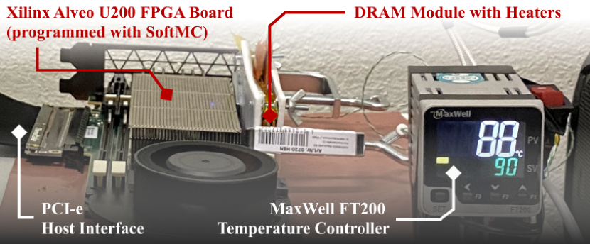
We conduct experiments on real DRAM chips444Due to time limitations, we conduct our tests on the 1) first 2K, 2) last 2K, and 3) middle 2K rows of Bank 0 in each DRAM chip, similar to [84, 129, 180]. using a modified version of SoftMC [43, 146] that can support DDR4 modules. Fig. 3 shows a picture of our experimental setup. We use the Xilinx Alveo U200 FPGA board [176], programmed with SoftMC to precisely issue DRAM commands.555SoftMC works with a minimum clock cycle of on Alveo U200 [176] and thus issues a DRAM command every in the double data rate domain. The host machine generates the sequence of DRAM commands that we issue to the DRAM module. To avoid fluctuations in ambient temperature, we place the DRAM module clamped with a pair of heaters on both sides. The heaters are controlled by a MaxWell FT200 [108] temperature controller that keeps DRAM chips at neighborhood of the target temperature.
Data Patterns. Our tests use four data patterns that are used by prior works [72, 102, 137, 79, 19, 22, 93, 73, 74, 75, 94]: 1) all ones (), 2) all zeros (), 3) alternating ones and zeros, i.e., checkerboard (), and 4) the inverse checkerboard ().
Disabling Sources of Interference. To directly observe whether HiRA reliably works at the circuit-level, we disable all known sources of interference (i.e., we prevent other DRAM error mechanisms (e.g., retention errors [102, 72, 110, 137, 140]) or error correction from interfering with a HiRA operation’s results) in three steps, similar to prior works [129, 79, 180]. First, we disable all DRAM self-regulation events (e.g., DRAM Refresh) and error mitigation mechanisms (e.g., error correction codes and RowHammer defense mechanisms) [60, 43, 175]) except calibration related events (e.g., ZQ calibration, which is required for signal integrity [60, 43]). Second, we conduct each test within a relatively short period of time () such that we do not observe retention errors. Third, we conduct each test for ten iterations to reduce noise in our measurements.
4.2 HiRA’s Coverage
HiRA works if the two rows that HiRA opens do not corrupt each other’s data. Therefore, it is important to carefully choose two DRAM rows for HiRA such that the rows are electrically isolated from each other, i.e., do not share a bitline or sense amplifier. The goal of our first experiment is to find all combinations of DRAM row pairs that HiRA can concurrently activate. To this end, we define HiRA’s coverage for a given row () in a given bank () as the fraction of other DRAM rows within which HiRA can reliably activate concurrently with . Algorithm 1 shows the experiment to find HiRA’s coverage for . To test a pair of DRAM rows and within , first, we initialize the two rows using inverse data patterns (lines 7–8). Second, we perform HiRA (lines 11–13) and close both rows (line 16). Third, we check whether there is a bit flip in either of the rows (lines 19–20). Fourth, if performing HiRA does not cause bit flips in either of the rows for any tested data pattern, we increment a counter called (line 25). Fifth, we calculate HiRA’s coverage for as the fraction of s that HiRA can concurrently activate with (line 26).
Fig. 4 shows the distribution of HiRA coverage across tested DRAM rows4 in a box and whiskers plot666A box-and-whiskers plot emphasizes the important metrics of a dataset’s distribution. The box is lower-bounded by the first quartile (i.e., the median of the first half of the ordered set of data points) and upper-bounded by the third quartile (i.e., the median of the second half of the ordered set of data points). The interquartile range () is the distance between the first and third quartiles (i.e., box size). Whiskers show the minimum and maximum values. for different combinations of (x-axis) and (colored boxes) timing parameters. The y-axis shows HiRA coverage across tested rows.
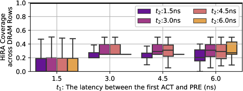
We make three observations from Fig. 4. First, if is or , a given DRAM row’s refresh operation can always be performed concurrently with at least another DRAM row’s refresh or activation (i.e., there are no DRAM rows with a HiRA coverage of ) for all tested values. Second, HiRA reliably parallelizes a tested row’s refresh operation with refresh or activation of any of the of the other rows777The minimum HiRA coverage we observe across all tested rows is when is and is either or . when is and is either or . Third, we observe that HiRA coverage can be if is chosen too small (e.g., ) or too large (e.g., ), meaning that at least one tested DRAM row’s refresh cannot be concurrently performed with refreshing or activating another tested DRAM row. We hypothesize that this happens because 1) is not long enough to enable sense amplifiers and 2) is not short enough for to interrupt row activation before the local row buffer is connected to the bank I/O or is too short for to disconnect ’s local row buffer from the bank I/O. Both design-induced variation [93] and manufacturing process-induced variation [19, 93] in row activation latency can cause this behavior. From these three observations, we conclude that it is possible to refresh a given DRAM row concurrently with refreshing or activating of the other DRAM rows on average when both and are . When HiRA is used with the configuration of , the latency of refreshing two rows is only (), while refreshing two rows with standard DRAM commands takes for 1) restoring the charge of the first row (), 2) precharging bitlines to prepare for second activation (), and 3) restoring the charge of the second row ().2 Therefore, HiRA reduces the latency of refreshing two rows by .
4.3 Verifying HiRA’s Second Row Activation
Observing no bit flips for a pair of rows tested using Algorithm 1 indicates either of the two cases: 1) HiRA successfully works or 2) HiRA activates only the first row because the DRAM chip simply ignores the second command. The goal of our second experiment is to test whether the DRAM chip ignores or performs HiRA’s second row activation command. To this end, we hammer the two adjacent rows888DRAM manufacturers use DRAM-internal mapping schemes to internally translate memory-controller-visible row addresses to physical row addresses [84, 155, 46, 70, 51, 102, 151, 73, 75, 93, 162, 9, 24, 136, 181, 129], which can vary across different DRAM modules. We reconstruct this mapping using single-sided RowHammer, similar to prior works [84, 79, 129, 180], so that we can hammer aggressor rows that are physically adjacent to a victim row. (i.e., aggressor rows) of a given victim row to induce RowHammer bit flips in the victim row (i.e., double-sided RowHammer [84, 79]). During the test, we try refreshing the victim row by using HiRA’s second row activation command. We hypothesize that if HiRA’s second row activation is not ignored (i.e., if HiRA works), then the minimum number of aggressor row activations required to induce the first RowHammer bit flip, i.e., RowHammer threshold (§2.4), increases compared to the RowHammer threshold measured without using HiRA. We measure RowHammer threshold of a given victim row via binary-search (similar to prior works [79, 129, 180]). Algorithm 2 shows how we perform a RowHammer test for a given victim row at a given hammer count () with and without a HiRA operation.
We conduct the RowHammer test in five steps. First, we initialize four DRAM rows in a given DRAM bank (BankX): the given victim row, a dummy row which HiRA can concurrently refresh with the given victim row, and the two aggressor rows. We initialize the victim row with the specified data pattern and the other three rows with the inverse data pattern (lines 3–9). Second, we hammer each aggressor row times (lines 12–16). Third, we either perform (lines 19–23) a HiRA operation (with HiRA) or wait (line 26) exactly the same amount of time as performing HiRA would take (without HiRA). Fourth, we hammer both aggressor rows times (lines 30–33). If HiRA’s second row activation is not ignored, then the victim row would be refreshed, and thus we would observe a significant increase in measured RowHammer threshold values in the test with HiRA, compared to the test without HiRA. Fifth, we read the victim row to check if the RowHammer test causes any bit flip (line 36).
Fig. 5 shows how a DRAM row’s RowHammer threshold varies when the row is refreshed using HiRA. Fig. 5a and 5b show the histogram of absolute and normalized RowHammer threshold values, respectively. We report the normalized values relative to tests without HiRA.
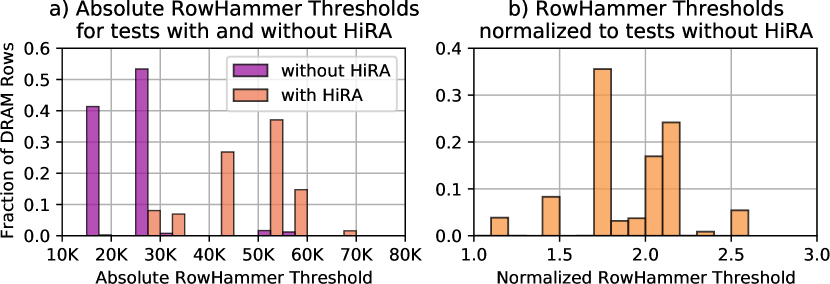
We make two observations. First, Fig. 5a shows that RowHammer threshold is / on average across tested rows when tested without / with HiRA. Second, Fig. 5b shows that RowHammer threshold increases by on average across tested DRAM rows and by more than 1.7 for the vast majority () of tested rows. Based on these two observations, we conclude that HiRA works in 56 tested DRAM chips (Table 1) such that HiRA’s second row activation, targeting the victim row, is not ignored, and thus the victim row is successfully activated concurrently with the dummy row.
4.4 Variation Across DRAM Banks
To investigate the variation in HiRA’s coverage and verify HiRA’s second row activation across DRAM banks, we repeat the tests that we explain in §4.2 and §4.3 for all 16 banks of three DRAM modules: A0, B0, and C0 (Table 1).
4.4.1 HiRA’s Coverage
We observe that the pairs of rows that HiRA can concurrently refresh and activate are identical across all 16 DRAM banks in all three modules. Based on this observation, we hypothesize that HiRA’s coverage largely depends on the DRAM circuit design, which should be a design-induced phenomenon across all DRAM banks.
4.4.2 Verifying HiRA’s Second Row Activation
To verify that HiRA’s second row activation works across all 16 DRAM banks, we repeat the tests shown in Algorithm 2. Fig. 6 shows how a DRAM row’s RowHammer threshold varies when the victim row is activated using HiRA’s second activation during a RowHammer attack (similar to Fig. 5b). The x-axis and different box colors show the module’s name and DRAM bank, respectively. The y-axis shows the measured RowHammer threshold in the tests with HiRA, normalized to the tests without HiRA. Each box in Fig. 6 shows the distribution’s and whiskers show the minimum and maximum values.6

We make three observations from Fig. 6. First, the normalized RowHammer threshold values are larger than across all banks in all three DRAM modules. Second, RowHammer threshold increases by , averaged across all banks in all three modules, when the victim row is refreshed using HiRA. Third, the average RowHammer threshold increase in a DRAM bank varies between and across all banks in all three modules. Therefore, we conclude that HiRA’s second row activation is not ignored in any bank.
5 HiRA-MC: HiRA Memory Controller
The HiRA Memory Controller (HiRA-MC)aims to improve overall system performance. To do so, HiRA-MC queues each periodic and preventive refresh request with a deadline and takes one of three possible actions in decreasing priority order: 1) concurrently perform a refresh operation with a memory access (refresh-access parallelization) before the refresh operation’s deadline; 2) concurrently perform a refresh operation with another refresh operation (refresh-refresh parallelization) if no memory access can be parallelized until the refresh operation’s deadline; or 3) perform a refresh operation by its deadline if the refresh operation cannot be concurrently performed with a memory access or another refresh. HiRA-MC intelligently schedules refresh operations from within the memory controller without requiring any modification to off-the-shelf DRAM chips.
Fig. 7 shows HiRA-MC’s components and their interaction with the memory request scheduler. First, we give an overview of HiRA-MC where we introduce its components. Then, we explain how HiRA-MC’s components interact with the memory request scheduler in performing four key operations.
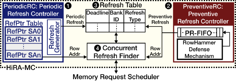
HiRA-MC Overview. HiRA-MC consists of four main components: Periodic Refresh Controller (PeriodicRC), Preventive Refresh Controller (PreventiveRC), Refresh Table, and Concurrent Refresh Finder. PeriodicRC generates a periodic refresh request for each DRAM row to maintain data integrity in the presence of DRAM cell charge leakage. To leverage HiRA’s subarray-level parallelism, PeriodicRC maintains a table called RefPtr table. RefPtr table has an entry per subarray, which contains a pointer to the next row to be refreshed within the corresponding subarray. PreventiveRC employs a refresh-based RowHammer defense mechanism (e.g., PARA [84]) to generate a preventive refresh request for a victim DRAM row. There might not be any memory access requests that can be parallelized with a periodic or preventive refresh when the refresh request is generated (i.e., there might not be any load or store memory requests waiting to be served by the memory controller). To address this issue, both PeriodicRC and PreventiveRC assign each refresh request a deadline that specifies the timestamp until which the refresh request must be performed. The deadline is determined using a configuration parameter called the maximum delay between the time a periodic/preventive refresh is generated and the time the refresh is performed (). The Refresh Table stores generated periodic and preventive refresh requests along with their deadline, target bank id, and refresh type (invalid, periodic, or preventive). The Concurrent Refresh Finder identifies the refresh requests that can be parallelized with memory access requests among the refresh requests stored in the Refresh Table. To serve a refresh request concurrently with a memory access request, the Concurrent Refresh Finder observes the memory access requests that the memory request scheduler999The memory request scheduler is the component that is responsible for scheduling DRAM requests, using a scheduling algorithm (e.g., FR-FCFS [143, 190] or PAR-BS [121]), and issuing DRAM commands to serve those requests. issues. If there is a refresh request that can be parallelized with a memory request, the Concurrent Refresh Finder replaces the memory request’s row activation command with a HiRA operation, such that HiRA’s first ACT targets the row that needs to be refreshed and HiRA’s second ACT targets the row that needs to be accessed. If HiRA-MC cannot perform a pending refresh request concurrently with a memory access until the refresh request’s deadline, the Concurrent Refresh Finder searches for another refresh request within the Refresh Table to parallelize the refresh request with. If possible, HiRA-MC performs a HiRA operation to concurrently refresh two rows. If the refresh request cannot be parallelized with an access or another refresh, HiRA-MC activates the row that needs to be refreshed and precharges the bank using nominal timing parameters.
5.1 HiRA-MC: Key Operations
5.1.1 Generating Periodic Refresh Requests
The Periodic Refresh Controller periodically generates refresh requests. PeriodicRC faces two main challenges in scheduling HiRA operations due to two fundamental differences between HiRA and operations. First, a command refreshes several rows in a DRAM bank as a batch [60, 61, 103]. In contrast, using the HiRA operation, the memory controller needs to issue an command for each refreshed DRAM row. Therefore, using HiRA increases DRAM bus utilization compared to using commands. For example, to refresh 64K rows in a bank of a DDR4 DRAM chip in , the memory controller issues 8K commands (once every [60]), indicating that each command refreshes eight rows in one bank. To ensure the same refresh rate as the baseline, PeriodicRC schedules 64K HiRA operations (once every ). Second, issuing a command triggers refresh operations in all banks in a rank (assuming all-bank refresh, as in DDR4 [60]). In contrast, HiRA operations are performed separately for each DRAM bank because they use already defined and commands at row- and bank-level, respectively. Therefore, frequently issued HiRA command sequences can occupy the command bus more than commands. For example, HiRA-MC needs to perform 128 HiRA operations to refresh the same number of rows as one command does in current systems, assuming that a single command refreshes eight rows from each of the 16 banks in a rank as in DDR4 [60]. To avoid overwhelming the command bus with HiRAoperations, PeriodicRC spreads the command bus pressure of HiRA command sequences over time by generating requests for each bank with the same period, starting at different time offsets. For example, assuming that 1) each bank receives a request once in every and 2) there are 16 banks, PeriodicRC generates a refresh request every (/16 banks) targeting a different bank. PeriodicRC inserts the generated request into the Refresh Table with the request’s 1) deadline, which is a timestamp pointing to the time that is later than the request’s generation time, 2) BankID, which is the target bank of the refresh request, and 3) refresh type, which is set to Periodic to indicate that the refresh request will perform a periodic refresh operation.
5.1.2 Generating Preventive Refresh Requests for RowHammer
HiRA-MC is not a RowHammer defense mechanism by itself, but it provides parallelism support for all memory controller-based preventive refresh mechanisms, which mitigate the RowHammer effect on victim rows by timely refreshing the victim rows [2, 84, 76, 5, 3, 7, 6, 157, 152, 185, 97, 135, 179, 33, 66, 42, 141, 82, 29, 98, 107, 189, 63]. HiRA-MC overlaps the latency of a preventive refresh operation with another periodic/preventive refresh or a memory access. To do so, PreventiveRC generates preventive refreshes with a large enough without compromising the security guarantees of RowHammer defense mechanisms. To achieve this, PreventiveRC assumes the worst case, where an attack fully exploits to maximize the hammer count such that the attack performs / additional activations during (after the preventive refresh is generated and before it is performed). To account for such case, PreventiveRC employs state-of-the-art RowHammer defense mechanisms[135, 66, 97, 152, 141, 82, 84, 157, 185] with a slightly increased aggressiveness in performing preventive refreshes. When implemented in PreventiveRC, the counter-based RowHammer defense mechanisms [135, 66, 97, 152, 141, 82] should be configured such that the mechanism triggers a preventive refresh at a hammer count that is / activations smaller than the mechanism’s original hammer count threshold (typically, the RowHammer threshold of the DRAM module). Therefore, even if the attack performs the maximum number of activations after the preventive refresh is generated, the total hammer count does not exceed the RowHammer defense mechanism’s original threshold before the preventive refresh is performed. When implemented in PreventiveRC, the probabilistic RowHammer defense mechanisms [84, 157, 185] should be configured with an increased probability threshold to maintain the same security guarantees as the original mechanism in the presence of . §9.1 explains how to increase the probability threshold to account for .
When the employed RowHammer defense mechanism generates a preventive refresh request, PreventiveRC 1) enqueues the refresh operation in a first-in-first-out queue, called PR-FIFO ( in Fig. 7), 2) creates an entry in the Refresh Table ( in Fig. 7) with the preventive refresh’s deadline and bank id, and 3) sets the request’s refresh type to Preventive to indicate that the refresh request will perform a preventive refresh operation.
5.1.3 Finding Concurrent Refresh Operations
Fig. 8 shows how HiRA-MC’s Concurrent Refresh Finder interacts with the memory request scheduler in two different cases: 1) when the memory request scheduler issues a command to prepare the bank for activating a ( in Fig. 8) and 2) when an internal timer periodically initiates a process that performs refreshes by their deadline ( in Fig. 8).
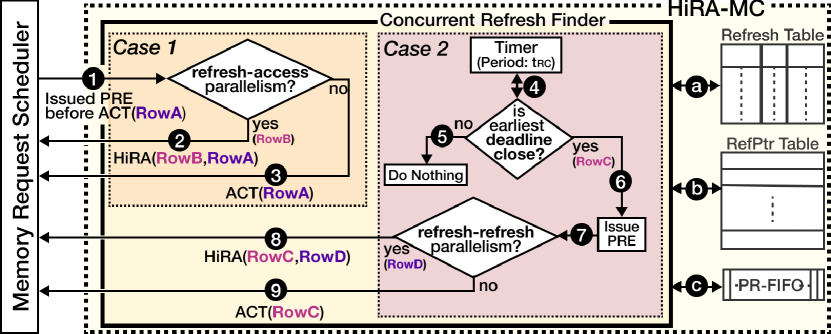
Case 1. To find an opportunity to concurrently refresh a DRAM row with a memory access (refresh-access parallelism), the Concurrent Refresh Finder observes the commands that the memory request scheduler issues. When the memory request scheduler issues a command to precharge the DRAM bank before activating a DRAM row () , the Concurrent Refresh Finder searches the Refresh Table (by iterating over the Refresh Table entries in the order of increasing deadlines) to find a refresh operation that targets the precharged bank ( ).
If the Refresh Table entry with the earliest deadline is a periodic refresh, the Concurrent Refresh Finder accesses the RefPtr Table ( ) to find a subarray 1) where refreshing a DRAM row can be parallelized with the activation of and 2) that has the smallest number of DRAM rows refreshed within the current refresh window. By doing so, HiRA-MC aims to advance the refresh pointers of all subarrays in a balanced manner while leveraging the subarray-level parallelism.
If the Refresh Table entry with the earliest deadline is a preventive refresh, the Concurrent Refresh Finder checks whether the request at the head of PR-FIFO can be refreshed concurrently with activating ( ).
If HiRA-MC finds a periodic or preventive refresh that targets and can be concurrently performed with an activation to ( ), the memory request scheduler issues a HiRAoperation such that the first and the second commands target and , respectively, so that is refreshed concurrently with activating .
If there is no opportunity to concurrently perform a periodic or preventive refresh with the activation of ( ), the memory request scheduler issues a regular command targeting . In this case, 1) the DRAM row activation is performed without leveraging HiRA’s parallelism because refresh-access parallelism is not possible and 2) the memory access request is prioritized over the queued refresh requests to improve system performance when queued refresh requests can be delayed until their deadline.
Case 2. To guarantee that each periodic and preventive refresh is performed timely (i.e., by its deadline), the Concurrent Refresh Finder periodically checks if there is a refresh operation that is close to its deadline (i.e., whose deadline is earlier than ) ( ). If there is no queued periodic or preventive refresh whose deadline is close ( ), the Concurrent Refresh Finder does not take any action. In doing so, HiRA-MC 1) does not interfere with the memory access requests and 2) opportunistically leaves refresh requests in the Refresh Table such that the refresh requests can be concurrently performed with a memory access by their deadlines.
If there is a refresh request (targeting a ) that needs to be performed within the next time window ( ), the Concurrent Refresh Finder precharges the target bank of the refresh operation if the bank is open and ( ) tries leveraging refresh-refresh parallelism by searching for a queued refresh operation that can be concurrently performed with refreshing . If there is a refresh request (targeting a ), which can be concurrently performed with refreshing (refresh-refresh parallelism), HiRA-MC forces the memory request scheduler to issue a HiRA operation such that the two activations of HiRA target and , respectively ( ). If such refresh-refresh parallelism is not possible ( ), the memory request scheduler issues a regular command targeting to perform the refresh operation because 1) refresh-refresh parallelism is not possible and 2) delaying ’s refresh would violate its deadline and could have caused bit flips.
5.1.4 Maintaining the Parallelism Information
To know if a DRAM row can be concurrently activated with another DRAM row, the memory controller needs to determine whether the two rows are located in subarrays that do not share bitlines or sense amplifiers. The memory controller can learn which subarrays do not share bitlines or a sense amplifiers with another subarray (i.e., determine the boundaries of a subarray) in two ways. First, the memory controller can perform a one-time reverse engineering (e.g., by testing for HiRA’s coverage as we do in §4.2). Second, DRAM manufacturers can expose this information to the memory controller by using mode status registers (MSRs) [60] in the DRAM chip. Once the memory controller obtains the subarray boundaries, it maintains them in a table called Subarray Pairs Table (SPT) implemented as an on-chip SRAM storage. SPT has an entry for each subarray (). This entry contains a list of subarrays which do not share bitlines or sense amplifiers with . Therefore, HiRA operation can be performed targeting a DRAM row in and another DRAM row in any of the listed subarrays.
5.2 Power Constraints
Each refresh and row activation in a HiRA operation is counted as a row activation with respect to the four row activation window () constraint in DDRx DRAM chips. We respect in our performance evaluation, such that within a given , at most four activations are performed in a DRAM rank (as required by DRAM datasheets (e.g., [60, 61, 57, 58])), thereby ensuring that the row activations are performed within the power budget of a DRAM rank.
5.3 Compatibility with Off-the-Shelf DRAM Chips
We experimentally demonstrate that HiRA works on all 56 real DRAM chips that we test (§4); and HiRA-MC does not require any modifications to these real DRAM chips to enable refresh-refresh and refresh-access parallelization.
5.4 Compatibility with Different Computing Systems
We discuss HiRA-MC’s compatibility with three types of computing systems: 1) FPGA-based systems (e.g., PiDRAM [126]), 2) contemporary processors, and 3) systems with programmable memory controllers [47, 12]. First, HiRA-MC can be easily integrated into all existing FPGA-based systems that use DRAM to store data [126, 177, 178] by implementing HiRA-MC in RTL. Second, contemporary processors require modifications to their memory controller logic to implement HiRA-MC. Implementing HiRA-MC is a design-time decision that requires balancing manufacturing cost with periodic and preventive refresh overhead reduction benefits. We show that HiRA-MC significantly improves system performance (§8 and §9) at low chip area cost (§6) and thus can be relatively easily integrated into contemporary processors. Third, systems that employ programmable controllers [47, 12] can be relatively easily modified to implement HiRA-MCby programming the HiRA operation and implementing HiRA-MC’s components using the ISA of programmable memory controllers [47, 12].
6 Hardware Complexity
We evaluate the hardware complexity of implementing HiRA-MC in a processor, using CACTI 7.0 [8] to model HiRA-MC’s components (Refresh Table, RefPtr Table, and PR-FIFO). We use CACTI’s technology node to model SRAM arrays for each component’s on-chip data storage. Table 2 shows the area cost and the access latency of each component.
| HiRA-MC Component | Area () | Area (*) | Access Latency |
|---|---|---|---|
| Refresh Table | < | ||
| RefPtr Table | |||
| PR-FIFO | < | ||
| Subarray Pairs Table (SPT) | |||
| Overall | ** |
Refresh Table. In this analysis, we assume a of 4because 1) increasing increases the hardware complexity of HiRA-MC (by increasing the number of entries in the Refresh Table and the PR-FIFO) and 2) a of 4already provides as large performance benefit as a of 8 (§8 and §9). Within a time window of 4, HiRA-MC can generate at most 4 periodic refresh requests per rank and 4 preventive refresh requests per bank (64 preventive refresh requests per rank). Therefore, a Refresh Table with 68 entries per rank is enough to store all generated refresh requests. Each entry consists of 1) 10 bits to store the deadline,101010 A 10-bit number can represent the number of clock cycles within a of 4 ( [60]), assuming a memory controller clock frequency of . 2) 4 bits to store the bank id, and 3) 2 bits to store the refresh type (Periodic, Preventive, or Invalid). Our analysis shows that Refresh Table consumes only chip area per rank and can be accessed in .
RefPtr Table. We model a 2048-entry RefPtr Table (128 entries per bank and 16 banks per rank). We assume that there can be as many as 1024 rows in a DRAM subarray. Thus, each RefPtr Table entry contains 10 bits to point to a row in a subarray. Based on our analysis, RefPtr Table’s size is chip area per rank and it can be accessed in .
PR-FIFO. We model a 4-entry PR-FIFO per DRAM bank, assuming the worst case, where the RowHammer defense mechanism generates a preventive refresh for every performed row activation. PR-FIFO’s chip area cost is per rank and access latency is .
Subarray Pairs Table (SPT). For 128 subarrays per bank, our analysis shows that this table can be accessed in and consumes only chip area per DRAM rank.
6.1 HiRA-MC’s Overall Area Overhead
HiRA-MC takes only chip area per DRAM rank. This area corresponds to of the chip area of a Intel processor [172].
6.2 HiRA-MC’s Overall Access Latency
In the worst-case, HiRA-MC traverses the Refresh Table to search for refresh-access parallelization opportunities. During traversal, within a time window, HiRA-MC accesses the Refresh Table and the SPT 68 times to iterate over all Refresh Table entries. Iterating over Refresh Table and SPT entries in a pipelined manner results in an overall latency of . If HiRA-MC finds a periodic refresh request, it accesses RefPtr Table once to get the address of the row that needs to be refreshed (see §5.1.3), which takes . If HiRA-MC finds a preventive refresh, it accesses the head of the PR-FIFO, which takes . Therefore, the overall access latency of HiRA-MC is , which is significantly smaller than the nominal of . We conclude that HiRA-MC completes all search operations with a significantly smaller latency than the latency of a precharge operation, and thus it does not cause additional latency for memory access requests.
7 Evaluation Methodology
We evaluate HiRA-MCvia two case studies focusing on high-density DRAM chips: 1) refreshing very high capacity DRAM chips and 2) protecting DRAM chips with high RowHammer vulnerability. We demonstrate for each study that HiRA-MCsignificantly improves system performance by leveraging HiRA’s ability to concurrently refresh a row while refreshing or activating another row.
Simulation Environment. To evaluate the performance impact of HiRA-MC under each use-case, we conduct cycle-level simulations, using Ramulator [144, 86]. Our baseline leverages the regular rank-level commands, periodically issued at every with a latency of in respect to DDR4 specifications [60]. Table 3 shows the simulated system configuration. In our evaluations, we assume a realistic system with 8 cores, connected to a memory rank with four bank groups each of which contains four banks (16 banks in total). We execute 125 8-core multiprogrammed workloads, randomly chosen from SPEC CPU2006 [159] benchmarks. We simulate these workloads until each core executes 200M instructions with a warmup period of 100M instructions, similar to prior work [79, 181]. The memory controller employs the FR-FCFS [143, 190] scheduling algorithm with the open-row policy. We assume that a refresh to a DRAM row can be served concurrently with a refresh or an access to of the rows within the same DRAM bank, based on our experimental results (§4.2). We measure system performance in terms of weighted speedup [31, 156].
| Processor | 3.2GHz, 8 core, 4-wide issue, 128-entry instr. window |
|---|---|
| Last-Level Cache | 64-byte cache line, 8-way set-associative, 8MB |
| Memory Controller | 64-entry each read and write request queues |
| Scheduling policy: FR-FCFS [143, 190] | |
| Address mapping: MOP [68] | |
| Main Memory | DDR4-2400 [60], 1 channel∗, 1 rank∗, 4 bank groups |
| 4 banks/bank group (16 banks per rank), 64K rows/bank | |
| Timing Parameters | , , |
Adapting Baseline Refresh for High-Capacity DRAM Chips. Across different generations of DRAM protocols [58, 61, 60, 57, 59] the minimum and maximum refresh interval () does not significantly change, while the standards allow the manufacturer to define the necessary refresh latency () value based on the time required to complete a refresh operation. As DRAM capacity increases, more DRAM rows need to be refreshed when a command is issued, which increases [124]. To estimate for a given density, we use the state-of-the-art regression model [124] for projecting with increased chip capacity (), as shown in Expression 1:
| (1) |
8 Periodic Refresh Results
We evaluate HiRA’s performance when HiRA is used for performing periodic refreshes in high-capacity DRAM chips instead of using conventional commands used in current systems. We sweep DRAM chip capacity and quantify the performance overhead of periodic refresh operations on a baseline system that performs rank-level operations and four configurations of HiRAwith different deadlines. Fig. 9 demonstrates system performance (y-axis) for different DRAM chip capacities from to (x-axis).
We denote HiRA’s different configurations as HiRA-N, where N specifies the configuration in terms of the number of row activations that can be performed within a , i.e., of HiRA-N is .
For example, HiRA-2 schedules each refresh request with a of , whereas HiRA-0 schedules refresh requests with a of 0 (i.e., the refresh operation must be performed immediately after it is generated by HiRA-MC). Fig. 9a shows system performance in terms of weighted speedup, normalized to an ideal system that we call No Refresh, where the system does not need to perform any periodic refreshes.
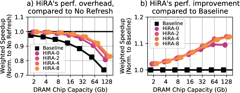
We make two observations from Fig. 9a. First, using commands to perform periodic refresh operations (as done in baseline) significantly degrades system performance as DRAM chip capacity increases. For example, periodic refresh operations cause system performance degradation for refreshing 128Gb DRAM chips on average across all evaluated workloads. Second, HiRA (HiRA-2) significantly reduces the performance degradation caused by periodic refresh operations by (from down to ), on average across all evaluated workloads for a DRAM chip capacity of 128Gb.
Fig. 9b shows system performance in terms of weighted speedup, normalized to the baseline. We make three observations from Fig. 9b. First, HiRA significantly improves system performance. For example, HiRA-2 provides performance improvement over the baseline on average across all evaluated workloads for a DRAM chip capacity of 128Gb. Second, HiRA’s performance benefits increase with up to a certain value of . For example, for a DRAM chip capacity of 128Gb, HiRA-0 and HiRA-2 provide and performance improvement over the baseline, respectively. This is because as increases, HiRA-MC can find more opportunities to perform each queued refresh operation concurrently with refreshing or accessing another DRAM row. We observe that increasing from to does not significantly improve system performance (i.e., curves for HiRA-2, HiRA-4, HiRA-8 overlap with each other) on average across all evaluated workloads. This is because a of is large enough to perform periodic refreshes concurrently with memory accesses or other refreshes. Third, HiRA’s performance improvement increases with DRAM chip capacity. For example, HiRA-2’s performance improvement increases from for 2Gb chips to for 128Gb chips on average across all evaluated workloads.
Based on these observations, we conclude that HiRA significantly improves system performance by reducing the performance overhead of periodic refresh operations, and HiRA’s benefits increase with DRAM chip capacity.
9 RowHammer Preventive Refresh Results
Modern DRAM chips, including the ones that are marketed as RowHammer-safe [33, 99, 113], are shown to be even more vulnerable to RowHammer (at the circuit level) than their predecessors [84, 119, 120, 79, 33, 42, 129, 54, 180, 27]. Therefore, it is critical for a RowHammer defense mechanism to efficiently scale with worsening RowHammer vulnerability. Among many RowHammer defense mechanisms (e.g., [2, 84, 76, 3, 5, 7, 6, 157, 152, 185, 97, 135, 179, 181, 33, 66, 42, 141, 147, 14, 89, 165, 36, 82, 98, 107, 189, 63, 64]), we find Probabilistic Row Activation (PARA) [84] as the most lightweight and hardware-scalable RowHammer defense due to two reasons. First, PARA’s hardware cost does not increase when it is scaled to work on chips that have higher RowHammer vulnerability. This is because PARA is a stateless mechanism that refreshes a potential victim row with a low probability, defined as PARA’s probability threshold (), when a DRAM row is activated, with no need for maintaining any metadata. Second, PARA, as a memory controller-based mechanism which is implemented solely in the processor chip, easily adapts to the RowHammer vulnerability of a given DRAM chip by programming after the processor is deployed. Unlike PARA, other defenses (e.g., [2, 84, 76, 3, 5, 7, 6, 157, 152, 185, 97, 135, 179, 181, 33, 66, 42, 141, 147, 14, 89, 165, 36, 82, 98, 107, 189, 63, 64]) are usually configured for a particular RowHammer vulnerability level at the processor chip’s design time and they cannot be easily reconfigured for a new DRAM chip’s RowHammer vulnerability. This is because these mechanisms require implementing as many hardware counters as needed to accurately identify a RowHammer attack for a given RowHammer threshold, and thus they likely need more counters to reliably work for smaller RowHammer thresholds; unfortunately, the number of hardware counters cannot be easily increased after deployment.
When scaled to work on a DRAM chip that has a higher RowHammer vulnerability, PARA refreshes a victim row with a higher probability, thereby inducing a larger system performance overhead [79, 181]. HiRA-MCreduces PARA’s performance overhead, by leveraging the parallelism HiRA provides. §9.1 explains how we configure when PARA is used with HiRA. Then, §9.2 evaluates HiRA’s performance when it is used for performing PARA’s preventive refreshes.
9.1 Security Analysis
9.1.1 Threat Model
We assume a comprehensive RowHammer threat model, similar to that assumed by state-of-the-art works [84, 135, 181], in which the attacker can 1) fully utilize memory bandwidth, 2) precisely time each memory request, and 3) comprehensively and accurately know details of the memory controller and the DRAM chip. We do not consider any hardware or software component to be trusted or safe except we assume that the DRAM commands issued by the memory controller are performed within the DRAM chip as intended.
9.1.2 Revisiting PARA’s configuration methodology
Kim et al. [84] configure PARA’s probability threshold (), assuming that the attacker hammers an aggressor row only enough times, but no more. With more than an order of magnitude decrease in the RowHammer threshold in the last decade[79, 33, 42, 129, 180], an attacker can complete a RowHammer attack 144 times within a refresh window of ,111111The minimum hammer count required to induce the first RowHammer bit flip (RowHammer threshold) for modern DRAM chips is as low as 9600 [79]. Assuming a of , performing 9600 row activations can be completed only in , which is 1/144.14 of a nominal refresh window of . As such, an attacker can perform 9600 activations for 144 times within a refresh window. requiring a revisit of PARA’s configuration methodology.121212A concurrent work also revisits PARA’s configuration methodology [148].
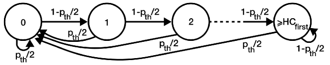
The rest of this section explains how we calculate for a given RowHammer threshold. Fig. 10 shows the probabilistic state machine that we use to calculate the hammer count, which we define as the number of aggressor row activations that may affect a victim row.Initially the hammer count is zero (state 0). When an aggressor row is activated, PARA triggers a preventive refresh with a probability of . Since there are two rows that are adjacent to the activated row, PARA refreshes the victim row with a probability of , in which case the hammer count is reset. Therefore, the hammer count is incremented with a probability of upon an aggressor row activation. An attack is considered to be successful if its hammer count reaches the RowHammer threshold () within a refresh window ().
Because the time delay between two row activations targeting the same bank cannot be smaller than , an attacker can perform a maximum of state transitions within a . To account for all possible access patterns, we model a successful RowHammer access pattern as a set of failed attempts, where the victim row is refreshed before the hammer count reaches the RowHammer threshold, followed by a successful attempt, where the victim row is not refreshed until the hammer count reaches the RowHammer threshold. To calculate , we follow a five-step approach. First, we calculate the probability of a failed attempt () and a successful attempt. Second, we calculate the probability of observing a number () of consecutive failed attempts.Third, we calculate the overall RowHammer success probability () as the overall probability of all possible successful RowHammer access patterns. Fourth, we extend the probability calculation to account for . Fifth, we calculate for a given failure probability target.
Step 1: Failed and successful attempts. Exp. 2 shows : the probability of a failed attempt with a given hammer count (). The attempt contains 1) consecutive aggressor row activations that do not trigger a preventive refresh, , where is smaller than the RowHammer threshold (), and 2) an aggressor row activation that triggers a preventive refresh .
| (2) |
Similarly, we calculate the probability of a successful attempt which has consecutive aggressor row activations that do not trigger a preventive refresh as .
Step 2: The probability of consecutive failed attempts. Since a failed attempt may have a hammer count value in the range , we account for all possible hammer count values that a failed attempt might have. Exp. 3 shows the probability of a given number of () consecutive failed attempts.
| (3) |
Step 3: Overall RowHammer success probability. To find the overall RowHammer success probability, we 1) calculate the probability of the successful RowHammer access pattern (), which consists of consecutive failed attempts and one successful attempt for each possible value that can take and 2) sum the probability of all possible successful RowHammer access patterns: . To do so, we multiply Exp. 3 with the probability of a successful attempt: . Exp. 4 shows how we calculate . We derive Exp. 4 by evaluating the product on both terms in Exp. 3: and .
| (4) |
To account for the worst-case, we maximize by choosing the worst possible value for each value. Intuitively, the number of activations in a failed attempt should be minimized. Since a failed attempt has to perform at least one activation, we conclude that all failed attempts fail after only one row activation in the worst case. Mathematically, our goal is to maximize . Since is a value between zero and one, we minimize the term to maximize . Thus, we derive Exp. 5 by choosing to achieve the maximum (worst-case) .
| (5) |
Exp. 6 shows the overall RowHammer success probability (), as the sum of all possible values. can be as small as 0 if the RowHammer attack does not include any failed attempt and as large as the maximum number of failed attempts that can fit in a refresh window () together with a successful attempt. Since in the worst case, each failed attempt costs only two row activations (): one aggressor row activation and one activation for preventively refreshing the victim row. Thus, the execution time of failed attempts, followed by one successful attempt is . Therefore, the maximum value can take within a refresh window () is .
| (6) |
Using Exps. 5 and 6, we compute the overall RowHammer success probability for a given PARA probability threshold ().
Step 4: Accounting for . The original PARA proposal [84] performs a preventive refresh immediately after the activated row is closed. However, HiRA-MC allows a preventive refresh to be queued for a time window as long as . Since the aggressor rows can be activated while a preventive refresh request is queued, we update Exps. 5 and 6, assuming the worst case, where an aggressor row is activated as many times as possible within (i.e., the maximum amount of time the preventive refresh is queued). To do so, we update Exp. 6: we reduce the RowHammer threshold () by the maximum number of activations that an attacker can perform within a (). Thus, we calculate and as shown in Exps. 7 and 8, respectively.
| (7) |
| (8) |
9.1.3 Results
We refer to the original PARA work [84] as PARA-Legacy. PARA-Legacy calculates the overall RowHammer success probability as with an optimistic assumption that the attacker hammers an aggressor row only enough times, but no more. To mathematically compare the overall RowHammer success probability that we calculate () with , we reorganize Exp. 8, which already includes , and derive Exp. 9.
| (9) |
Exp. 9 shows that is a multiple of by a factor of , where depends on a given system’s properties (e.g., ) and PARA’s configuration (e.g., ). To understand the difference between and , we evaluate Exp. 9 for different RowHammer threshold values.131313We calculate for , , and . For old DRAM chips (manufactured in 2010-2013) [84], is 1.0005 (for and [84]), causing only variation in PARA’s reliability target. However,for future DRAM chips with values of 1024 and 64 ( values of 0.4730 and 0.8341), becomes 1.0331 and 1.3212, respectively. Therefore, the difference between the two probabilities, and , significantly increases as RowHammer worsens.
Fig. 11a shows how decreasing RowHammer threshold, i.e., worsening RowHammer vulnerability (x-axis), changes PARA’s probability threshold () (y-axis). The dashed curve shows PARA-Legacy’s probability threshold (calculated using ), whereas the other curves show for different values which we calculate using Exp. 8.
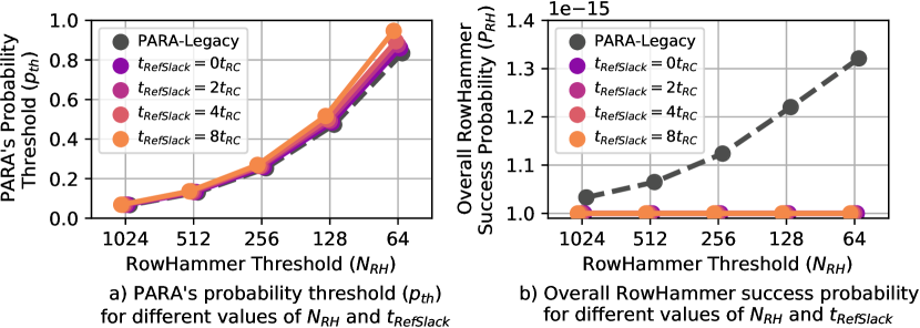
We make two observations from Fig. 11a. First, to maintain a RowHammer success probability, significantly increases for smaller RowHammer thresholds. For example, increases from 0.068 to 0.860 ( =0) when the RowHammer threshold reduces from 1024 to 64. This is because as the RowHammer threshold reduces, fewer activations are enough for an attack to induce bit flips. Thus, PARA needs to perform preventive refreshes more aggressively. Second, increases with , e.g., when the RowHammer threshold is 128, should be 0.48, 0.49, 0.50, and 0.52 for values of 0, 2, 4, and 8, respectively. This is because a larger allows reaching a higher hammer count, requiring PARA to perform preventive refreshes more aggressively.
Fig. 11b shows how decreasing RowHammer threshold () changes the overall RowHammer success probability (). We calculate all values by evaluating Exp. 8 using the values in Fig. 11a. The dashed curve shows PARA-Legacy’s , whereas the other curves show PARA’s for different configurations. We make two observations from Fig. 11b. First, configuring as described in PARA-Legacy [84] 1) results in a larger overall RowHammer success probability than the consumer memory reliability target (), and 2) the difference between and the increases as the RowHammer vulnerability increases (i.e., the RowHammer threshold reduces). For example, the values that PARA-Legacy calculates targeting a overall RowHammer success probability for RowHammer thresholds of 1024 and 64, result in overall RowHammer success probability values of and , respectively. This happens because PARA-Legacy assumes that the attacker performs only as many aggressor row activations as the RowHammer threshold () within a refresh window, even though increasingly more aggressor row activations can be performed in a refresh window as reduces. Second, the values that we calculate using Exp. 8 significantly reduce the overall RowHammer success probability compared to PARA-Legacy (and maintains a of across all RowHammer thresholds) because Exp. 8, to calculate , takes into account all aggressor row activations that can be performed in a refresh window.
We conclude that as RowHammer threshold decreases, PARA-Legacy’s values result in a significantly larger overall RowHammer success probability than the consumer memory reliability target (), while values calculated using Exp. 8 maintain the overall RowHammer success probability at .
9.2 Performance of PARA with HiRA
We evaluate HiRA’s performance benefits when it is used to perform PARA’s preventive refreshes. We use the evaluation methodology described in §7. We calculate values Exp. 8. We evaluate PARA’s impact on performance when it is used with and without HiRA for different RowHammer thresholds.
Fig. 12a shows the performance of 1) a system that implements PARA without HiRA, labeled as PARA, and 2) a system that implements PARA with four different configurations of HiRA, labeled using the HiRA-N notation ( of HiRA-N is ) as HiRA-0, HiRA-2, HiRA-4, and HiRA-8, normalized to the baseline that does not perform any preventive refresh operations (i.e., does not implement PARA).
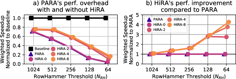
From Fig. 12a, we observe that PARA induces slowdown on system performance on average across all evaluated workloads when it is configured for a RowHammer threshold of 1024. HiRA-2 reduces PARA’s performance overhead down to , which results in a performance improvement of compared to PARA. Similarly, when configured for a RowHammer threshold of 64, HiRA-4 increases system performance by compared to PARA as it reduces PARA’s performance overhead by (from down to ). This happens because HiRA reduces the latency of preventive refreshes by concurrently performing them with refreshing or accessing other rows in the same bank.
Fig. 12b shows the performance of the system that implements PARA with HiRA (labeled using the HiRA-N notation), normalized to the performance of the system that implements PARA without HiRA (labeled as PARA). We make two observations from Fig. 12b. First, HiRA’s performance improvement increases with higher RowHammer vulnerability, i.e., smaller RowHammer threshold. For example, when compared to PARA (Fig. 12b), HiRA-2 provides a speedup of on average across all evaluated workloads when RowHammer threshold is 64, which is significantly larger than HiRA-2’s performance improvement of when RowHammer threshold is 1024. This is because PARA generates preventive refreshes more aggressively as RowHammer threshold reduces (§9.1.2), which increases PARA’s memory bandwidth utilization and provides HiRA with a larger number of preventive refreshes to parallelize with other accesses and refreshes. Second, configuring HiRA with a larger improves system performance. For example, when the RowHammer threshold is , HiRA-0, HiRA-2, HiRA-4, and HiRA-8 improve system performance by , , , and , respectively, on average across all evaluated workloads, compared to PARA without HiRA (Fig. 12b). This happens because HiRA-MC can find a parallelization opportunity for a queued preventive refresh with a larger probability when there is a larger .
Based on our observations, we conclude that HiRA significantly reduces PARA’s system performance degradation.
10 Sensitivity Studies
We analyze how HiRA’s performance changes with 1) number of channels and 2) number of ranks per channel. To evaluate high-end system configurations, we sweep the number of channels and ranks from one to eight, inspired by commodity systems [49, 48, 112, 60, 113, 114].
10.1 HiRA with Periodic Refresh
Fig. 13 shows how increasing the number of channels (x-axis) affects HiRA’s performance for two configurations (HiRA-2 and HiRA-4), compared to the baseline, where rows are periodically refreshed using rank-level command. The y-axis shows system performance in terms of average weighted speedup across 125 evaluated workloads, normalized to the baseline’s performance at the 1-channel 1-rank configuration. Three subplots show the results for 2Gb (left), 8Gb (middle), and 32Gb (right) DRAM chip capacity.
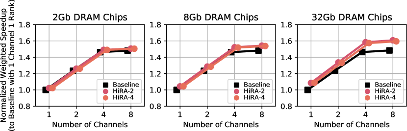
We make three observations. First, both the baseline and HiRA provide higher performance with more channels. For example, HiRA and the baseline exhibit speedups of and , respectively, when the number of channels increases from one to eight for a DRAM chip capacity of 32Gb. This is because memory-level parallelism increases with more channels. Performance overheads of rank-level refresh and HiRA do not increase with more channels because different channels do not share command, address, or data buses, thereby allowing different channels to be accessed simultaneously. Second, at smaller channel counts, the effect of channel count on performance is greater. For example, the slopes of the line plots are steeper in-between one and four channels than in-between four and eight channels. This happens because the evaluated workloads do not exhibit sufficient memory-level parallelism to fully leverage the available parallelism with more than four channels. Third, both HiRA-2 and HiRA-4 configurations exhibit significant speedup over the baseline for all channel counts. For example, HiRA-2 improves the performance of a system using 32Gb DRAM chips with eight channels by compared to the baseline with 8-channels. We conclude that HiRA provides significant performance benefits for high-capacity DRAM chips even with a large number of channels.
Fig. 14 shows how increasing the number of ranks (x-axis) affects HiRA’s performance benefits. The y-axis shows system performance using the same metric as Fig. 13 uses. Three subplots show the results for 2Gb (left), 8Gb (middle), and 32Gb (right) DRAM chip capacity.
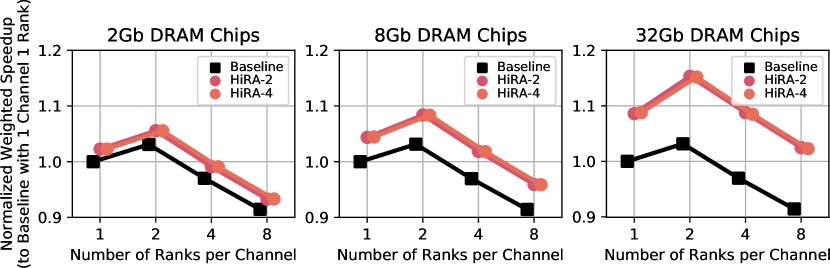
We make three observations. First, increasing the number of ranks from one to two increases system performance (e.g., by and for the baseline and HiRA-2, respectively, for a chip capacity of 32Gb). This is because the evaluated workloads leverage the higher rank-level parallelismSecond, unlike with channels, further increasing the number of ranks beyond two slows down the system for both the baseline and HiRA by and , respectively, on average as number of ranks increases from 2 to 8. This happens because multiple ranks share a single command bus and together occupy the command bus for refresh operations, making the command bus a bottleneck. Third, HiRA provides higher performance than the baseline for all evaluated rank configurations. For example, HiRA-2 provides performance improvement over the baseline even for an 8-rank system with 32Gb DRAM chips. We conclude that HiRA provides significant performance benefits for high-capacity DRAM chips compared to the baseline even with a large number of ranks.
10.2 HiRA with Preventive Refresh
Fig. 15 shows how increasing the channel count (x-axis) affects PARA’s impact on system performance when used without HiRA (labeled as PARA) and with HiRA (labeled as HiRA-N, where N represents the configuration as in §8 and §9.2). The y-axis reports system performance in terms of average weighted speedup across 125 workloads, normalized to the baseline 1-channel 1-rank system with no RowHammer defense mechanism. Three subplots show the results for RowHammer thresholds () of 1024 (left), 256 (middle), and 64 (right).
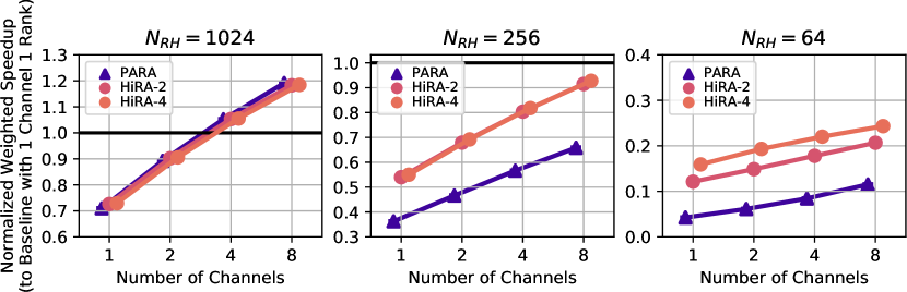
We make three observations. First, system performance increases with channel count when PARA is used (with and without HiRA). For example, increasing the number of channels from one to eight improves the performance of the system with PARA and HiRA-2 by and by , respectively, when the RowHammer threshold is 1024. This is because memory accesses are distributed across a larger number of banks given more channels, thereby reducing the congestion in banks, and thus the number of row buffer conflicts. As a result, the evaluated workloads perform fewer row activations, and PARA generates fewer preventive refreshes. Second, at smaller RowHammer thresholds, HiRA significantly improves system performance even with a large number of channels. For example, PARA causes performance reduction on an eight-channel system when the RowHammer threshold is 64. HiRA-2 and HiRA-4 reduce this performance overhead to and , respectively, by performing preventive refreshes concurrently with refreshing or activating other rows in the same bank. Third, HiRA improves system performance compared to PARA for all evaluated channel counts. This happens because HiRA reduces the performance overhead of PARA’s preventive refreshes for each memory channel regardless of the system’s channel count. We conclude that HiRA provides significant performance benefits even with a large number of channels.
Fig. 16 shows how increasing the rank count (x-axis) affects PARA’s impact on system performance when used without HiRA and with HiRA. The y-axis shows system performance using the same metric as Fig. 15 uses. Three subplots show the results for RowHammer thresholds () of 1024 (left), 256 (middle), and 64 (right).
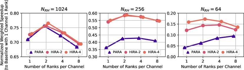
We make three observations. First, similar to Fig. 14, increasing the number of ranks from one to two increases system performance for all three mechanisms (e.g., by and for PARA and HiRA-4 when ) across all shown RowHammer thresholds due to the higher rank-level parallelism. Second, further increasing the number of ranks beyond two ranks reduces HiRA’s benefits over PARA. This happens because increasing the rank count beyond two increases the command bus bandwidth usage of periodic refresh requests.Third, despite the performance reduction at high rank counts, HiRA significantly improves system performance compared to PARA. For example, HiRA-2 (HiRA-4) improves system performance by () compared to PARA on an 8-rank system with a RowHammer threshold of 64. Based on these observations, we conclude that HiRA provides significant performance benefits over PARA even when a large number of ranks share the command bus.
11 Summary of Major Results
We summarize the major observations from four main evaluations in this paper. First, by using HiRA, it is possible to reliably refresh a DRAM row concurrently with refreshing or activating another DRAM row within the same bank in off-the-shelf DRAM chips (§4). §4 experimentally demonstrates on real DRAM chips that HiRAcan reliably parallelize a DRAM row’s refresh operation with refresh or activation of any of the of the rows within the same bank. Second, HiRA-MC reduces the overall latency of refreshing two DRAM rows within the same bank by (§4). Third, HiRAsignificantly improves system performance by reducing the performance degradation caused by periodic refreshes across all system configurations we evaluate (§8). Fourth, HiRA-MCsignificantly improves system performance by reducing the performance overhead of PARA’s preventive refreshes across all system configurations we evaluate (§9). Our major results show that HiRA can effectively and robustly improve system performance by reducing the time spent for both periodic refreshes and preventive refreshes without compromising system reliability or security. We hope that our findings inspire DRAM manufacturers and standards bodies to explicitly and properly support HiRA in future DRAM chips.
12 Limitations
We identify HiRA’s limitations under three categories.
First, we experimentally demonstrate that HiRA is supported by real DDR4 DRAM chips. However, we cannot verify the exact operation of HiRA (i.e., how HiRA is enabled) in those chips for two reasons: 1) no public documentation discloses or verifies HiRA in real DRAM chips and 2) we do not have access to DRAM manufacturers’ proprietary circuit designs.
Second, all DRAM chips that exhibit successful HiRA operation are manufactured by SK Hynix (the second largest DRAM manufacturer that has of the DRAM market share [160]). We also conducted experiments using 40 DRAM chips from each of the two other manufacturers (Samsung and Micron) for which we observed no successful HiRA operation. We hypothesize that the DRAM chips from these other manufacturers ignore the or the second command of HiRA’s command sequence when and timing parameters are greatly violated (e.g., the DRAM chip acts as if it did not receive the or the second commands). Therefore, HiRA is currently limited to DRAM chips that can successfully perform HiRA operations. We believe that other DRAM chips are fundamentally capable of HiRA since HiRA is consistent with fundamental operational principles of modern DRAM. We hope that this work inspires future DRAM designs that explicitly support HiRA, given that HiRA 1) provides significant performance benefits and 2) is already possible in real DRAM chips, even though DRAM chips are not even designed to support it. Third, performing periodic refresh using HiRA results in higher memory command bus utilization compared to using conventional REF commands. HiRA issues a row activation (ACT) command and a precharge (PRE) command to refresh a single DRAM row, while multiple DRAM rows are refreshed when a single REF command is issued. Even though HiRA overlaps the latency of row activation and precharge operations with the latency of other refresh or access operations, it still uses the command bus bandwidth to transmit and commands to DRAM chips. As the number of ranks and banks per DRAM channel increases, HiRA’s command bus utilization can cause memory access requests to experience larger delays compared to using REF commands (as we evaluate in §10). However, HiRA still provides system performance benefit over a baseline memory controller that uses REF commands even in an 8-rank system with high command bus utilization.
We conclude that none of these limitations fundamentally prevent a system designer from using existing DRAM chips that can reliably perform HiRA operations and thus, benefit from HiRA’s refresh-refresh and refresh-access parallelization.
13 Related Work
To our knowledge, this is the first work to demonstrate that 1) real off-the-shelf DRAM chips are capable of refreshing a DRAM row concurrently with refreshing or activating another row within the same DRAM bank, by carefully violating DRAM timing parameters and 2) doing so is beneficial to reduce the performance overhead of both periodic refresh operations (required for reliable DRAM operation) and preventive refresh operations (required for RowHammer bit flip prevention). We classify the related work into six main categories.
Eliminating unnecessary refreshes (e.g., [103, 100, 123, 4, 140, 137, 166, 75, 73, 72, 50, 104, 74, 65, 52, 69, 173, 35, 158, 30, 117, 44, 91, 132, 168, 83]). Various prior works eliminate unnecessary refresh operations by leveraging the heterogeneity in the retention time of DRAM cells to reduce the rate at which some or all DRAM rows are refreshed. Our work differs from these works in two key aspects. First, most of these works rely on identifying cells or rows with worst-case retention times, which is a difficult problem [115, 116, 137, 103, 140, 102]. In contrast, our work uses a relatively simple and well-understood one-time experiment to 1) identify HiRA’s coverage and 2) verify that HiRA reliably works, presented in §4.2 and §4.3, respectively. Second, these works focus on reducing the performance overhead of periodic refreshes, but not the increasingly worsening performance overhead of preventive refresh operations of RowHammer defenses [79, 42, 129, 179, 181, 135, 141]. In contrast, our work tackles the performance overheads of both periodic and preventive refreshes.
Circuit-level modifications to reduce the performance impact of refresh operations (e.g., [40, 105, 80, 81, 182, 125, 122, 128, 23]). These works develop DRAM-based techniques that 1) reduce the latency of a refresh operation [40, 105], 2) implement a new refresh command that can be interrupted to quickly perform main memory accesses [122], and 3) reduce the rate at which some or all DRAM rows are refreshed [80, 81, 182, 125]. As opposed to HiRA, these techniques 1) are not compatible with existing DRAM chips as they require modifications to DRAM circuitry, and 2) cannot hide DRAM access latency in the presence of refresh operations.
Memory access scheduling techniques to reduce the performance impact of refresh operations (e.g., [118, 161, 20, 131, 130, 90]). Several works propose issuing commands during DRAM idle time (where no memory access requests are scheduled) to reduce the performance impact of refresh operations. Most of these works leverage the flexibility of delaying a command for multiple refresh intervals (e.g., for in DDR4 [60]). In contrast, HiRA overlaps the latency of a refresh operation with other refreshes or memory accesses and thus can reduce the performance impact of refresh operations without relying on DRAM idle time.
Modifications to the DRAM architecture to leverage subarray-level parallelism (e.g., [85, 20, 169, 186]). Several works partially overlap the latency of refresh operations or memory accesses via modifications to the DRAM architecture. The HiRA operation builds on the basic ideas of subarray-level parallelism introduced in [85] and refresh-access parallelization introduced in [20, 186]. However, unlike HiRA, these works require modifications to DRAM chip design, and thus they are not compatible with off-the-shelf DRAM chips. In contrast, HiRA uses existing and commands, and we demonstrate that it works on real off-the-shelf DRAM chips.
RowHammer defense mechanisms that use preventive refresh operations (e.g., [2, 84, 76, 5, 3, 7, 6, 157, 152, 185, 97, 135, 179, 33, 66, 42, 141, 82, 29, 98, 107, 189, 63]). These works propose mechanisms that observe memory access patterns and speculatively schedule preventive refresh operations targeting potential victim rows of a RowHammer attack. HiRA can be combined with all of these mechanisms to reduce the performance overheads of preventive refresh operations.
Reducing the latency of major DRAM operations (e.g., [41, 26, 170, 187, 154, 95, 94, 77, 19, 22, 93, 18, 153]). Many works develop techniques that reduce the latency of major DRAM operations (e.g., , , , ) by leveraging 1) temporal locality in workload access patterns [41, 26, 170, 187, 154], 2) the guardbands in manufacturer-recommended DRAM timing parameters [95, 94, 77, 19, 93, 22], and 3) variation in DRAM latency due to temperature dependence [18, 94, 77]. These latency reduction techniques can improve system performance by alleviating the performance impact of refresh operations (e.g., a refresh can be performed faster with a reduced charge restoration latency). These techniques can be combined with HiRA to further alleviate the performance impact of refresh operations, as HiRA overlaps the latency of refreshing a DRAM row with the latency of refreshing or activating another row in the same bank.
14 Conclusion
We introduce HiRA, a new DRAM operation that can reliably parallelize a DRAM row’s refresh operation with refresh or activation of another row within the same bank. HiRA achieves this by activating two electrically-isolated rows in quick succession, allowing them to be refreshed/activated without disturbing each other. We show that HiRA 1) works reliably in 56 real off-the-shelf DRAM chips, using already-available (i.e., standard) and DRAM commands, by violating timing constraints and 2) reduces the overall latency of refreshing two rows by . To leverage the parallelism HiRAprovides, we design the HiRA Memory Controller (HiRA-MC). HiRA-MC modifies the memory request scheduler to perform HiRA operations when a periodic or RowHammer-preventive refresh can be performed concurrently with another refresh or row activation to the same bank. Our system-level evaluations show that HiRA-MC increases system performance by and as it reduces the performance degradation due to periodic and preventive refreshes, respectively. We conclude that HiRA1) already works in off-the-shelf DRAM chips and can be used to significantly reduce the performance degradation caused by both periodic and preventive refreshes and 2) provides higher performance benefits in higher-capacity DRAM chips. We hope that our findings will inspire DRAM manufacturers and standards bodies to explicitly and properly support HiRA in future DRAM chips and standards.
Acknowledgments
We thank our shepherd and the reviewers of ASPLOS’22, ISCA’22, and MICRO’22 for valuable feedback. We thank the SAFARI Research Group members for useful feedback and the stimulating intellectual environment they provide. We acknowledge the generous gifts provided by our industrial partners, including Google, Huawei, Intel, Microsoft, and VMware, and support from the Microsoft Swiss Joint Research Center.
References
- [1] M. T. Aga, Z. B. Aweke, and T. Austin, “When Good Protections Go Bad: Exploiting Anti-DoS Measures to Accelerate Rowhammer Attacks,” in HOST, 2017.
- [2] Apple Inc., “About the Security Content of Mac EFI Security Update 2015-001,” https://support.apple.com/en-us/HT204934, June 2015.
- [3] Z. B. Aweke, S. F. Yitbarek, R. Qiao, R. Das, M. Hicks, Y. Oren, and T. Austin, “ANVIL: Software-Based Protection Against Next-Generation Rowhammer Attacks,” in ASPLOS, 2016.
- [4] S. Baek, S. Cho, and R. Melhem, “Refresh Now and Then,” IEEE TC, 2013.
- [5] K. Bains, J. Halbert, C. Mozak, T. Schoenborn, and Z. Greenfield, “Row Hammer Refresh Command,” 2015, U.S. Patent 9,117,544.
- [6] K. S. Bains and J. B. Halbert, “Distributed Row Hammer Tracking,” 2016, U.S. Patent 9,299,400.
- [7] K. S. Bains and J. B. Halbert, “Row Hammer Monitoring Based on Stored Row Hammer Threshold Value,” 2016, U.S. Patent 9,384,821.
- [8] R. Balasubramonian, A. B. Kahng, N. Muralimanohar, A. Shafiee, and V. Srinivas, “CACTI 7: New Tools for Interconnect Exploration in Innovative Off-Chip Memories,” ACM TACO, 2017.
- [9] A. Barenghi, L. Breveglieri, N. Izzo, and G. Pelosi, “Software-Only Reverse Engineering of Physical DRAM Mappings for Rowhammer Attacks,” in IVSW, 2018.
- [10] R. Baumann, “Radiation-Induced Soft Errors in Advanced Semiconductor Technologies,” IEEE TDMR, 2005.
- [11] S. Bhattacharya and D. Mukhopadhyay, “Curious Case of Rowhammer: Flipping Secret Exponent Bits Using Timing Analysis,” in CHES, 2016.
- [12] M. N. Bojnordi and E. Ipek, “PARDIS: A Programmable Memory Controller for the DDRx Interfacing Standards,” in ISCA, 2012.
- [13] E. Bosman, K. Razavi, H. Bos, and C. Giuffrida, “Dedup Est Machina: Memory Deduplication as An Advanced Exploitation Vector,” in S&P, 2016.
- [14] F. Brasser, L. Davi, D. Gens, C. Liebchen, and A.-R. Sadeghi, “Can’t Touch This: Software-Only Mitigation Against Rowhammer Attacks Targeting Kernel Memory,” in USENIX Security, 2017.
- [15] W. Burleson, O. Mutlu, and M. Tiwari, “Invited: Who is the Major Threat to Tomorrow’s Security? You, the Hardware Designer,” in DAC, 2016.
- [16] Y. Cai, S. Ghose, E. F. Haratsch, Y. Luo, and O. Mutlu, “Error Characterization, Mitigation, and Recovery in Flash Memory Based Solid-State Drives,” Proc. IEEE, 2017.
- [17] Y. Cai, E. F. Haratsch, O. Mutlu, and K. Mai, “Error Patterns in MLC NAND Flash Memory: Measurement, Characterization, and Analysis,” in DATE, 2012.
- [18] K. Chandrasekar, S. Goossens, C. Weis, M. Koedam, B. Akesson, N. Wehn, and K. Goossens, “Exploiting Expendable Process-Margins in DRAMs for Run-Time Performance Optimization,” in DATE, 2014.
- [19] K. K. Chang, A. Kashyap, H. Hassan, S. Ghose, K. Hsieh, D. Lee, T. Li, G. Pekhimenko, S. Khan, and O. Mutlu, “Understanding Latency Variation in Modern DRAM Chips: Experimental Characterization, Analysis, and Optimization,” in SIGMETRICS, 2016.
- [20] K. K. Chang, D. Lee, Z. Chishti, A. R. Alameldeen, C. Wilkerson, Y. Kim, and O. Mutlu, “Improving DRAM Performance by Parallelizing Refreshes with Accesses,” in HPCA, 2014.
- [21] K. K. Chang, P. J. Nair, D. Lee, S. Ghose, M. K. Qureshi, and O. Mutlu, “Low-Cost Inter-Linked Subarrays (LISA): Enabling Fast Inter-Subarray Data Movement in DRAM,” in HPCA, 2016.
- [22] K. K. Chang, A. G. Yağlıkçı, S. Ghose, A. Agrawal, N. Chatterjee, A. Kashyap, D. Lee, M. O’Connor, H. Hassan, and O. Mutlu, “Understanding Reduced-Voltage Operation in Modern DRAM Devices: Experimental Characterization, Analysis, and Mechanisms,” in SIGMETRICS, 2017.
- [23] H. Choi, D. Hong, J. Lee, and S. Yoo, “Reducing DRAM Refresh Power Consumption by Runtime Profiling of Retention Time and Dual-Row Activation,” Microprocessors and Microsystems, 2020.
- [24] L. Cojocar, J. Kim, M. Patel, L. Tsai, S. Saroiu, A. Wolman, and O. Mutlu, “Are We Susceptible to Rowhammer? An End-to-End Methodology for Cloud Providers,” in S&P, 2020.
- [25] L. Cojocar, K. Razavi, C. Giuffrida, and H. Bos, “Exploiting Correcting Codes: On the Effectiveness of ECC Memory Against Rowhammer Attacks,” in S&P, 2019.
- [26] A. Das, H. Hassan, and O. Mutlu, “VRL-DRAM: Improving DRAM Performance via Variable Refresh Latency,” in DAC, 2018.
- [27] F. de Ridder, P. Frigo, E. Vannacci, H. Bos, C. Giuffrida, and K. Razavi, “SMASH: Synchronized Many-Sided Rowhammer Attacks from JavaScript,” in USENIX Security, 2021.
- [28] R. H. Dennard, “Field-Effect Transistor Memory,” 1968, U.S. Patent 3,387,286.
- [29] F. Devaux and R. Ayrignac, “Method and Circuit for Protecting a DRAM Memory Device from the Row Hammer Effect,” 2021, 10,885,966.
- [30] P. G. Emma, W. R. Reohr, and M. Meterelliyoz, “Rethinking Refresh: Increasing Availability and Reducing Power in DRAM for Cache Applications,” IEEE Micro, 2008.
- [31] S. Eyerman and L. Eeckhout, “System-Level Performance Metrics for Multiprogram Workloads,” IEEE Micro, 2008.
- [32] P. Frigo, C. Giuffrida, H. Bos, and K. Razavi, “Grand Pwning Unit: Accelerating Microarchitectural Attacks with the GPU,” in S&P, 2018.
- [33] P. Frigo, E. Vannacci, H. Hassan, V. van der Veen, O. Mutlu, C. Giuffrida, H. Bos, and K. Razavi, “TRRespass: Exploiting the Many Sides of Target Row Refresh,” in S&P, 2020.
- [34] F. Gao, G. Tziantzioulis, and D. Wentzlaff, “ComputeDRAM: In-Memory Compute Using Off-the-Shelf DRAMs,” in MICRO, 2019.
- [35] M. Ghosh and H.-H. S. Lee, “Smart Refresh: An Enhanced Memory Controller Design for Reducing Energy in Conventional and 3D Die-Dtacked DRAMs,” in MICRO, 2007.
- [36] Z. Greenfield and T. Levy, “Throttling Support for Row-Hammer Counters,” 2016, U.S. Patent 9,251,885.
- [37] D. Gruss, M. Lipp, M. Schwarz, D. Genkin, J. Juffinger, S. O’Connell, W. Schoechl, and Y. Yarom, “Another Flip in the Wall of Rowhammer Defenses,” in S&P, 2018.
- [38] D. Gruss, C. Maurice, and S. Mangard, “Rowhammer.js: A Remote Software-Induced Fault Attack in Javascript,” arXiv:1507.06955 [cs.CR], 2016.
- [39] GSKill, “F4-2400C17S-8GNT Specifications,” https://www.gskill.com/product/165/186/1535961538/F4-2400C17S-8GNT.
- [40] H. Hassan, M. Patel, J. S. Kim, A. G. Yağlıkçı, N. Vijaykumar, N. Mansouri Ghiasi, S. Ghose, and O. Mutlu, “CROW: A Low-Cost Substrate for Improving DRAM Performance, Energy Efficiency, and Reliability,” in ISCA, 2019.
- [41] H. Hassan, G. Pekhimenko, N. Vijaykumar, V. Seshadri, D. Lee, O. Ergin, and O. Mutlu, “ChargeCache: Reducing DRAM Latency by Exploiting Row Access Locality,” in HPCA, 2016.
- [42] H. Hassan, Y. C. Tugrul, J. S. Kim, V. van der Veen, K. Razavi, and O. Mutlu, “Uncovering In-DRAM RowHammer Protection Mechanisms: A New Methodology, Custom RowHammer Patterns, and Implications,” in MICRO, 2021.
- [43] H. Hassan, N. Vijaykumar, S. Khan, S. Ghose, K. Chang, G. Pekhimenko, D. Lee, O. Ergin, and O. Mutlu, “SoftMC: A Flexible and Practical Open-Source Infrastructure for Enabling Experimental DRAM Studies,” in HPCA, 2017.
- [44] J. Hong, H. Kim, and S. Kim, “EAR: ECC-Aided Refresh Reduction through 2-D Zero Compression,” in PACT, 2018.
- [45] S. Hong, P. Frigo, Y. Kaya, C. Giuffrida, and T. Dumitraş, “Terminal Brain Damage: Exposing the Graceless Degradation in Deep Neural Networks Under Hardware Fault Attacks,” in USENIX Security, 2019.
- [46] M. Horiguchi, “Redundancy Techniques for High-Density DRAMs,” in ISIS, 1997.
- [47] T. Hussain, A. Haider, and E. Ayguadé, “PMSS: A Programmable Memory System and Scheduler for Complex Memory Patterns,” JPDC, 2014.
- [48] A. Inc., “AMD EPYC™ 7003 Series Processors,” https://www.amd.com/system/files/documents/amd-epyc-7003-series-datasheet.pdf.
- [49] Intel Inc., “3rd Gen Intel Xeon Scalable Processors,” https://www.intel.com/content/dam/www/public/us/en/documents/a1171486-icelake-productbrief-updates-r1v2.pdf.
- [50] C. Isen and L. John, “ESKIMO - Energy Savings Using Semantic Knowledge of Inconsequential Memory Occupancy for DRAM Subsystem,” in MICRO, 2009.
- [51] K. Itoh, VLSI Memory Chip Design. Springer, 2001.
- [52] S. M. A. H. Jafri, H. Hassan, A. Hemani, and O. Mutlu, “Refresh Triggered Computation: Improving the Energy Efficiency of Convolutional Neural Network Accelerators,” TACO, 2021.
- [53] Y. Jang, J. Lee, S. Lee, and T. Kim, “SGX-Bomb: Locking Down the Processor via Rowhammer Attack,” in SOSP, 2017.
- [54] P. Jattke, V. van der Veen, P. Frigo, S. Gunter, and K. Razavi, “Blacksmith: Scalable Rowhammering in the Frequency Domain,” in S&P, 2022.
- [55] JEDEC, JESD79F: Double Data Rate (DDR) SDRAM Standard, 2008.
- [56] JEDEC, JEP122G: Failure Mechanisms and Models for Semiconductor Devices, 2012.
- [57] JEDEC, JESD209-4B: Low Power Double Data Rate 4 (LPDDR4) Standard, 2017.
- [58] JEDEC, JESD209-5A: LPDDR5 SDRAM Standard, 2020.
- [59] JEDEC, JESD235C: High Bandwidth Memory (HBM) DRAM, 2020.
- [60] JEDEC, JESD79-4C: DDR4 SDRAM Standard, 2020.
- [61] JEDEC, JESD79-5: DDR5 SDRAM Standard, 2020.
- [62] S. Ji, Y. Ko, S. Oh, and J. Kim, “Pinpoint Rowhammer: Suppressing Unwanted Bit Flips on Rowhammer Attacks,” in ASIACCS, 2019.
- [63] B. K. Joardar, T. K. Bletsch, and K. Chakrabarty, “Learning to Mitigate RowHammer Attacks,” in DATE, 2022.
- [64] J. Juffinger, L. Lamster, A. Kogler, M. Eichlseder, M. Lipp, and D. Gruss, “CSI: Rowhammer–Cryptographic Security and Integrity against Rowhammer (to appear),” in S&P, 2023.
- [65] M. Jung, E. Zulian, D. M. Mathew, M. Herrmann, C. Brugger, C. Weis, and N. Wehn, “Omitting Refresh: A Case Study for Commodity and Wide I/O DRAMs,” in MEMSYS, 2015.
- [66] I. Kang, E. Lee, and J. H. Ahn, “CAT-TWO: Counter-Based Adaptive Tree, Time Window Optimized for DRAM Row-Hammer Prevention,” IEEE Access, 2020.
- [67] U. Kang, H.-S. Yu, C. Park, H. Zheng, J. Halbert, K. Bains, S. Jang, and J. S. Choi, “Co-Architecting Controllers and DRAM to Enhance DRAM Process Scaling,” in The Memory Forum, 2014.
- [68] D. Kaseridis, J. Stuecheli, and L. K. John, “Minimalist Open-Page: A DRAM Page-Mode Scheduling Policy for the Many-Core Era,” in MICRO, 2011.
- [69] Y. Katayama, E. J. Stuckey, S. Morioka, and Z. Wu, “Fault-Tolerant Refresh Power Reduction of DRAMs for Quasi-Nonvolatile Data Retention,” in EFT, 1999.
- [70] B. Keeth and R. Baker, DRAM Circuit Design: A Tutorial. Wiley, 2001.
- [71] B. Keeth, R. J. Baker, B. Johnson, and F. Lin, DRAM Circuit Design: Fundamental and High-Speed Topics. John Wiley & Sons, 2007.
- [72] S. Khan, D. Lee, Y. Kim, A. R. Alameldeen, C. Wilkerson, and O. Mutlu, “The Efficacy of Error Mitigation Techniques for DRAM Retention Failures: A Comparative Experimental Study,” in SIGMETRICS, 2014.
- [73] S. Khan, D. Lee, and O. Mutlu, “PARBOR: An Efficient System-Level Technique to Detect Data-Dependent Failures in DRAM,” in DSN, 2016.
- [74] S. Khan, C. Wilkerson, D. Lee, A. R. Alameldeen, and O. Mutlu, “A Case for Memory Content-Based Detection and Mitigation of Data-Dependent Failures in DRAM,” CAL, 2016.
- [75] S. Khan, C. Wilkerson, Z. Wang, A. R. Alameldeen, D. Lee, and O. Mutlu, “Detecting and Mitigating Data-Dependent DRAM Failures by Exploiting Current Memory Content,” in MICRO, 2017.
- [76] D.-H. Kim, P. J. Nair, and M. K. Qureshi, “Architectural Support for Mitigating Row Hammering in DRAM Memories,” CAL, 2014.
- [77] J. S. Kim, M. Patel, H. Hassan, and O. Mutlu, “Solar-DRAM: Reducing DRAM Access Latency by Exploiting the Variation in Local Bitlines,” in ICCD, 2018.
- [78] J. S. Kim, M. Patel, H. Hassan, L. Orosa, and O. Mutlu, “D-RaNGe: Using Commodity DRAM Devices to Generate True Random Numbers with Low Latency and High Throughput,” in HPCA, 2019.
- [79] J. S. Kim, M. Patel, A. G. Yağlıkçı, H. Hassan, R. Azizi, L. Orosa, and O. Mutlu, “Revisiting RowHammer: An Experimental Analysis of Modern Devices and Mitigation Techniques,” in ISCA, 2020.
- [80] J. Kim and M. C. Papaefthymiou, “Dynamic Memory Design for Low Data-Retention Power,” in PATMOS, 2000.
- [81] J. Kim and M. Papaefthymiou, “Block-Based Multiperiod Dynamic Memory Design for Low Data-Retention Power,” TVLSI, 2003.
- [82] M. J. Kim, J. Park, Y. Park, W. Doh, N. Kim, T. J. Ham, J. W. Lee, and J. H. Ahn, “Mithril: Cooperative Row Hammer Protection on Commodity DRAM Leveraging Managed Refresh,” in HPCA, 2022.
- [83] S. Kim, W. Kwak, C. Kim, D. Baek, and J. Huh, “Charge-Aware DRAM Refresh Reduction with Value Transformation,” in HPCA, 2020.
- [84] Y. Kim, R. Daly, J. Kim, C. Fallin, J. H. Lee, D. Lee, C. Wilkerson, K. Lai, and O. Mutlu, “Flipping Bits in Memory Without Accessing Them: An Experimental Study of DRAM Disturbance Errors,” in ISCA, 2014.
- [85] Y. Kim, V. Seshadri, D. Lee, J. Liu, and O. Mutlu, “A Case for Exploiting Subarray-Level Parallelism (SALP) in DRAM,” in ISCA, 2012.
- [86] Y. Kim, W. Yang, and O. Mutlu, “Ramulator: A Fast and Extensible DRAM Simulator,” CAL, 2016.
- [87] Kingston, “KSM32RD8/16HDR Specifications,” https://www.kingston.com/dataSheets/KSM32RD8_16HDR.pdf, 2020.
- [88] A. Kogler, J. Juffinger, S. Qazi, Y. Kim, M. Lipp, N. Boichat, E. Shiu, M. Nissler, and D. Gruss, “Half-Double: Hammering From the Next Row Over,” in USENIX Security, 2022.
- [89] R. K. Konoth, M. Oliverio, A. Tatar, D. Andriesse, H. Bos, C. Giuffrida, and K. Razavi, “ZebRAM: Comprehensive and Compatible Software Protection Against Rowhammer Attacks,” in OSDI, 2018.
- [90] J. B. Kotra, N. Shahidi, Z. A. Chishti, and M. T. Kandemir, “Hardware-Software Co-Design to Mitigate DRAM Refresh Overheads: A Case for Refresh-Aware Process Scheduling,” ASPLOS, 2017.
- [91] K. Kraft, C. Sudarshan, D. M. Mathew, C. Weis, N. Wehn, and M. Jung, “Improving the Error Behavior of DRAM by Exploiting its Z-channel Property,” in DATE, 2018.
- [92] A. Kwong, D. Genkin, D. Gruss, and Y. Yarom, “RAMBleed: Reading Bits in Memory Without Accessing Them,” in S&P, 2020.
- [93] D. Lee, S. Khan, L. Subramanian, S. Ghose, R. Ausavarungnirun, G. Pekhimenko, V. Seshadri, and O. Mutlu, “Design-Induced Latency Variation in Modern DRAM Chips: Characterization, Analysis, and Latency Reduction Mechanisms,” in SIGMETRICS, 2017.
- [94] D. Lee, Y. Kim, G. Pekhimenko, S. Khan, V. Seshadri, K. Chang, and O. Mutlu, “Adaptive-Latency DRAM: Optimizing DRAM Timing for the Common-Case,” in HPCA, 2015.
- [95] D. Lee, Y. Kim, V. Seshadri, J. Liu, L. Subramanian, and O. Mutlu, “Tiered-Latency DRAM: A Low Latency and Low Cost DRAM Architecture,” in HPCA, 2013.
- [96] D. Lee, L. Subramanian, R. Ausavarungnirun, J. Choi, and O. Mutlu, “Decoupled Direct Memory Access: Isolating CPU and IO Traffic by Leveraging a Dual-Data-Port DRAM,” in PACT, 2015.
- [97] E. Lee, I. Kang, S. Lee, G. E. Suh, and J. H. Ahn, “TWiCe: Preventing Row-Hammering by Exploiting Time Window Counters,” in ISCA, 2019.
- [98] G.-H. Lee, S. Na, I. Byun, D. Min, and J. Kim, “CryoGuard: A Near Refresh-Free Robust DRAM Design for Cryogenic Computing,” in ISCA, 2021.
- [99] J. Lee, “Green Memory Solution,” Investor’s Forum, Samsung Electronics, 2014.
- [100] C.-H. Lin, D.-Y. Shen, Y.-J. Chen, C.-L. Yang, and M. Wang, “SECRET: Selective Error Correction for Refresh Energy Reduction in DRAMs,” in ICCD, 2012.
- [101] M. Lipp, M. T. Aga, M. Schwarz, D. Gruss, C. Maurice, L. Raab, and L. Lamster, “Nethammer: Inducing Rowhammer Faults Through Network Requests,” arXiv:1805.04956 [cs.CR], 2018.
- [102] J. Liu, B. Jaiyen, Y. Kim, C. Wilkerson, O. Mutlu, J. Liu, B. Jaiyen, Y. Kim, C. Wilkerson, and O. Mutlu, “An Experimental Study of Data Retention Behavior in Modern DRAM Devices,” in ISCA, 2013.
- [103] J. Liu, B. Jaiyen, R. Veras, and O. Mutlu, “RAIDR: Retention-Aware Intelligent DRAM Refresh,” in ISCA, 2012.
- [104] S. Liu, K. Pattabiraman, T. Moscibroda, and B. G. Zorn, “Flikker: Saving DRAM Refresh-Power through Critical Data Partitioning,” in ASPLOS, 2011.
- [105] H. Luo, T. Shahroodi, H. Hassan, M. Patel, A. G. Yağlıkçı, L. Orosa, J. Park, and O. Mutlu, “CLR-DRAM: A Low-Cost DRAM Architecture Enabling Dynamic Capacity-Latency Trade-Off,” in ISCA, 2020.
- [106] Y. Luo, S. Ghose, Y. Cai, E. F. Haratsch, and O. Mutlu, “Enabling Accurate and Practical Online Flash Channel Modeling for Modern MLC NAND Flash Memory,” in JSAC, 2016.
- [107] M. Marazzi, P. Jattke, F. Solt, and K. Razavi, “ProTRR: Principled yet Optimal In-DRAM Target Row Refresh,” in S&P, 2022.
- [108] Maxwell, “FT20X User Manual,” https://www.maxwell-fa.com/upload/files/base/8/m/311.pdf.
- [109] Memory.NET, “HMAA4GU6AJR8N,” https://memory.net/product/hmaa4gu6ajr8n-xn-sk-hynix-1x-32gb-ddr4-3200-udimm-pc4-25600u-dual-rank-x8-module/.
- [110] J. Meza, Q. Wu, S. Kumar, and O. Mutlu, “Revisiting Memory Errors in Large-Scale Production Data Centers: Analysis and Modeling of New Trends from the Field,” in DSN, 2015.
- [111] R. Micheloni, P. Onufryk, A. Marelli, C. Norrie, and I. Jaser, “Apparatus and Method Based on LDPC Codes for Adjusting a Correctable Raw Bit Error Rate Limit in a Memory System,” 2015, U.S. Patent 9,092,353.
- [112] Micron Inc., “DDR4 Module Part Numbering System,” https://media-www.micron.com/-/media/client/global/documents/products/part-numbering-guide/numsdrammod.pdf?la=en&rev=79e3864cbeac4be190fa3c619a12bddb.
- [113] Micron Inc., “SDRAM, 4Gb: x4, x8, x16 DDR4 SDRAM Features,” 2014.
- [114] Micron Inc., “TN-40-03: DDR4 Networking Design Guide,” 2014.
- [115] I. Mrozek, “Analysis of Multibackground Memory Testing Techniques,” IJAMCS, 2010.
- [116] I. Mrozek, Multi-Run Memory Tests for Pattern Sensitive Faults. Springer, 2019.
- [117] L. Mukhanov, K. Tovletoglou, H. Vandierendonck, D. S. Nikolopoulos, and G. Karakonstantis, “Workload-Aware DRAM Error Prediction Using Machine Learning,” in IISWC, 2019.
- [118] J. Mukundan, H. Hunter, K.-h. Kim, J. Stuecheli, and J. F. Martínez, “Understanding and Mitigating Refresh Overheads in High-Density DDR4 DRAM Systems,” in ISCA, 2013.
- [119] O. Mutlu, “The RowHammer Problem and Other Issues We May Face as Memory Becomes Denser,” in DATE, 2017.
- [120] O. Mutlu and J. S. Kim, “RowHammer: A Retrospective,” TCAD, 2019.
- [121] O. Mutlu and T. Moscibroda, “Parallelism-Aware Batch Scheduling: Enhancing Both Performance and Fairness of Shared DRAM Systems,” in ISCA, 2008.
- [122] P. J. Nair, C.-C. Chou, and M. K. Qureshi, “Refresh Pausing in DRAM Memory Systems,” TACO, 2014.
- [123] P. J. Nair, D.-H. Kim, and M. K. Qureshi, “ArchShield: Architectural Framework for Assisting DRAM Scaling by Tolerating High Error Rates,” in ISCA, 2013.
- [124] K. Nguyen, K. Lyu, X. Meng, V. Sridharan, and X. Jian, “Nonblocking Memory Refresh,” in ISCA, 2018.
- [125] T. Ohsawa, K. Kai, and K. Murakami, “Optimizing the DRAM Refresh Count for Merged DRAM/Logic LSIs,” in ISLPED, 1998.
- [126] A. Olgun, J. G. Luna, K. Kanellopoulos, B. Salami, H. Hassan, O. Ergin, and O. Mutlu, “PiDRAM: A Holistic End-to-end FPGA-based Framework for Processing-in-DRAM,” TACO, 2022.
- [127] A. Olgun, M. Patel, A. G. Yağlıkçı, H. Luo, J. S. Kim, N. Bostanci, N. Vijaykumar, O. Ergin, and O. Mutlu, “QUAC-TRNG: High-Throughput True Random Number Generation Using Quadruple Row Activation in Commodity DRAM Chips,” in ISCA, 2021.
- [128] L. Orosa, Y. Wang, M. Sadrosadati, J. S. Kim, M. Patel, I. Puddu, H. Luo, K. Razavi, J. Gómez-Luna, H. Hassan, N. Mansouri-Ghiasi, S. Ghose, and O. Mutlu, “CODIC: A Low-Cost Substrate for Enabling Custom In-DRAM Functionalities and Optimizations,” in ISCA, 2021.
- [129] L. Orosa, A. G. Yağlıkçı, H. Luo, A. Olgun, J. Park, H. Hassan, M. Patel, J. S. Kim, and O. Mutlu, “A Deeper Look into RowHammer’s Sensitivities: Experimental Analysis of Real DRAM Chips and Implications on Future Attacks and Defenses,” in MICRO, 2021.
- [130] X. Pan and F. Mueller, “Hiding DRAM Refresh Overhead in Real-Time Cyclic Executives,” in RTSS, 2019.
- [131] X. Pan and F. Mueller, “The Colored Refresh Server for DRAM,” in ISORC, 2019.
- [132] H. Park, S. Yoo, and S. Lee, “Power Management of Hybrid DRAM/PRAM-based Main Memory,” in DAC, 2011.
- [133] K. Park, C. Lim, D. Yun, and S. Baeg, “Experiments and Root Cause Analysis for Active-Precharge Hammering Fault in DDR3 SDRAM under 3xnm Technology,” Microelectronics Reliability, 2016.
- [134] K. Park, D. Yun, and S. Baeg, “Statistical Distributions of Row-Hammering Induced Failures in DDR3 Components,” Microelectronics Reliability, 2016.
- [135] Y. Park, W. Kwon, E. Lee, T. J. Ham, J. H. Ahn, and J. W. Lee, “Graphene: Strong yet Lightweight Row Hammer Protection,” in MICRO, 2020.
- [136] M. Patel, J. Kim, T. Shahroodi, H. Hassan, and O. Mutlu, “Bit-Exact ECC Recovery (BEER): Determining DRAM On-Die ECC Functions by Exploiting DRAM Data Retention Characteristics,” in MICRO, 2020.
- [137] M. Patel, J. S. Kim, and O. Mutlu, “The Reach Profiler (REAPER): Enabling the Mitigation of DRAM Retention Failures via Profiling at Aggressive Conditions,” in ISCA, 2017.
- [138] P. Pessl, D. Gruss, C. Maurice, M. Schwarz, and S. Mangard, “DRAMA: Exploiting DRAM Addressing for Cross-CPU Attacks,” in USENIX Security, 2016.
- [139] R. Qiao and M. Seaborn, “A New Approach for RowHammer Attacks,” in HOST, 2016.
- [140] M. Qureshi, D.-H. Kim, S. Khan, P. Nair, and O. Mutlu, “AVATAR: A Variable-Retention-Time (VRT) Aware Refresh for DRAM Systems,” in DSN, 2015.
- [141] M. Qureshi, A. Rohan, G. Saileshwar, and P. J. Nair, “Hydra: Enabling Low-Overhead Mitigation of Row-Hammer at Ultra-Low Thresholds via Hybrid Tracking,” in ISCA, 2022.
- [142] K. Razavi, B. Gras, E. Bosman, B. Preneel, C. Giuffrida, and H. Bos, “Flip Feng Shui: Hammering a Needle in the Software Stack,” in USENIX Security, 2016.
- [143] S. Rixner, W. J. Dally, U. J. Kapasi, P. Mattson, and J. D. Owens, “Memory Access Scheduling,” in ISCA, 2000.
- [144] SAFARI Research Group, “Ramulator — GitHub Repository,” https://github.com/CMU-SAFARI/ramulator.
- [145] SAFARI Research Group, “RowHammer — GitHub Repository,” https://github.com/CMU-SAFARI/rowhammer.
- [146] SAFARI Research Group, “SoftMC — GitHub Repository,” https://github.com/CMU-SAFARI/softmc.
- [147] G. Saileshwar, B. Wang, M. Qureshi, and P. J. Nair, “Randomized Row-Swap: Mitigating Row Hammer by Breaking Spatial Correlation Between Aggressor and Victim Rows,” in ASPLOS, 2022.
- [148] S. Saroiu and A. Wolman, “How to Configure Row-Sampling-Based Rowhammer Defenses,” DRAMSec, 2022.
- [149] M. Seaborn and T. Dullien, “Exploiting the DRAM Rowhammer Bug to Gain Kernel Privileges,” Black Hat, 2015.
- [150] V. Seshadri, Y. Kim, C. Fallin, D. Lee, R. Ausavarungnirun, G. Pekhimenko, Y. Luo, O. Mutlu, P. B. Gibbons, M. A. Kozuch, and T. Mowry, “RowClone: Fast and Energy-Efficient In-DRAM Bulk Data Copy and Initialization,” in MICRO, 2013.
- [151] V. Seshadri, T. Mullins, A. Boroumand, O. Mutlu, P. B. Gibbons, M. A. Kozuch, and T. C. Mowry, “Gather-Scatter DRAM: In-DRAM Address Translation to Improve the Spatial Locality of Non-Unit Strided Accesses,” in MICRO, 2015.
- [152] S. M. Seyedzadeh, A. K. Jones, and R. Melhem, “Mitigating Wordline Crosstalk Using Adaptive Trees of Counters,” in ISCA, 2018.
- [153] W. Shin, J. Choi, J. Jang, J. Suh, Y. Moon, Y. Kwon, and L.-S. Kim, “DRAM-Latency Optimization Inspired by Relationship between Row-Access Time and Refresh Timing,” IEEE TC, 2015.
- [154] W. Shin, J. Yang, J. Choi, and L.-S. Kim, “NUAT: A Non-Uniform Access Time Memory Controller,” in HPCA, 2014.
- [155] R. T. Smith, J. D. Chlipala, J. F. Bindels, R. G. Nelson, F. H. Fischer, and T. F. Mantz, “Laser Programmable Redundancy and Yield Improvement in a 64K DRAM,” JSSC, 1981.
- [156] A. Snavely and D. M. Tullsen, “Symbiotic Job Scheduling for A Simultaneous Multithreaded Processor,” in ASPLOS, 2000.
- [157] M. Son, H. Park, J. Ahn, and S. Yoo, “Making DRAM Stronger Against Row Hammering,” in DAC, 2017.
- [158] S. P. Song, “Method and System for Selective DRAM Refresh to Reduce Power Consumption,” 2000, U.S. Patent 6,094,705.
- [159] Standard Performance Evaluation Corp., “SPEC CPU 2006,” http://www.spec.org/cpu2006/.
- [160] Statista, “DRAM Manufacturers Revenue Share Worldwide From 2011 to 2022, by Quarter,” https://www.statista.com/statistics/271726/global-market-share-held-by-dram-chip-vendors-since-2010/, 2022.
- [161] J. Stuecheli, D. Kaseridis, H. C.Hunter, and L. K. John, “Elastic Refresh: Techniques to Mitigate Refresh Penalties in High Density Memory,” in MICRO, 2010.
- [162] A. Tatar, C. Giuffrida, H. Bos, and K. Razavi, “Defeating Software Mitigations Against Rowhammer: A Surgical Precision Hammer,” in RAID, 2018.
- [163] M. C. Tol, S. Islam, B. Sunar, and Z. Zhang, “Toward Realistic Backdoor Injection Attacks on DNNs using RowHammer,” arXiv:2110.07683v2 [cs.LG], 2022.
- [164] V. van der Veen, Y. Fratantonio, M. Lindorfer, D. Gruss, C. Maurice, G. Vigna, H. Bos, K. Razavi, and C. Giuffrida, “Drammer: Deterministic Rowhammer Attacks on Mobile Platforms,” in CCS, 2016.
- [165] V. van der Veen, M. Lindorfer, Y. Fratantonio, H. P. Pillai, G. Vigna, C. Kruegel, H. Bos, and K. Razavi, “GuardION: Practical Mitigation of DMA-Based Rowhammer Attacks on ARM,” in DIMVA, 2018.
- [166] R. Venkatesan, S. Herr, and E. Rotenberg, “Retention-Aware Placement in DRAM (RAPID): Software Methods for Quasi-Non-Volatile DRAM,” in HPCA, 2006.
- [167] A. J. Walker, S. Lee, and D. Beery, “On DRAM RowHammer and the Physics on Insecurity,” IEEE TED, 2021.
- [168] S. Wang, M. N. Bojnordi, X. Guo, and E. Ipek, “Content Aware Refresh: Exploiting the Asymmetry of DRAM Retention Errors to Reduce the Refresh Frequency of Less Vulnerable Data,” IEEE TC, 2018.
- [169] Y. Wang, L. Orosa, X. Peng, Y. Guo, S. Ghose, M. Patel, J. S. Kim, J. G. Luna, M. Sadrosadati, N. M. Ghiasi et al., “FIGARO: Improving System Performance via Fine-Grained In-DRAM Data Relocation and Caching,” in MICRO, 2020.
- [170] Y. Wang, A. Tavakkol, L. Orosa, S. Ghose, N. M. Ghiasi, M. Patel, J. S. Kim, H. Hassan, M. Sadrosadati, and O. Mutlu, “Reducing DRAM Latency via Charge-Level-Aware Look-Ahead Partial Restoration,” in MICRO, 2018.
- [171] Z. Weissman, T. Tiemann, D. Moghimi, E. Custodio, T. Eisenbarth, and B. Sunar, “JackHammer: Efficient Rowhammer on Heterogeneous FPGA–CPU Platforms,” arXiv:1912.11523 [cs.CR], 2020.
- [172] WikiChip, “Core i7-5960X Extreme Edition - Intel.” [Online]. Available: https://en.wikichip.org/wiki/intel/core_i7ee/i7-5960x
- [173] C. Wilkerson, A. R. Alameldeen, Z. Chishti, W. Wu, D. Somasekhar, and S.-l. Lu, “Reducing Cache Power with Low-Cost, Multi-Bit Error-Correcting Codes,” in ISCA, 2010.
- [174] Y. Xiao, X. Zhang, Y. Zhang, and R. Teodorescu, “One Bit Flips, One Cloud Flops: Cross-VM Row Hammer Attacks and Privilege Escalation,” in USENIX Security, 2016.
- [175] Xilinx Inc., “UltraScale Architecture-Based FPGAs Memory IP v1.4,” https://www.xilinx.com/support/documentation/ip_documentation/ultrascale_memory_ip/v1_4/pg150-ultrascale-memory-ip.pdf.
- [176] Xilinx Inc., “Xilinx Alveo U200 FPGA Board,” https://www.xilinx.com/products/boards-and-kits/alveo/u200.html.
- [177] Xilinx Inc., “Adaptable Accelerator Cards for Data Center Workloads,” 2021. [Online]. Available: https://www.xilinx.com/products/boards-and-kits/alveo.html
- [178] Xilinx Inc., “FPGAs and 3D ICs,” 2021. [Online]. Available: https://www.xilinx.com/products/silicon-devices/fpga.html
- [179] A. G. Yağlıkçı, J. S. Kim, F. Devaux, and O. Mutlu, “Security Analysis of the Silver Bullet Technique for RowHammer Prevention,” arXiv:2106.07084 [cs.CR], 2021.
- [180] A. G. Yağlıkçı, H. Luo, G. F. De Oliviera, A. Olgun, M. Patel, J. Park, H. Hassan, J. S. Kim, L. Orosa, and O. Mutlu, “Understanding RowHammer Under Reduced Wordline Voltage: An Experimental Study Using Real DRAM Devices,” in DSN, 2022.
- [181] A. G. Yağlıkçı, M. Patel, J. S. Kim, R. Azizibarzoki, A. Olgun, L. Orosa, H. Hassan, J. Park, K. Kanellopoullos, T. Shahroodi, S. Ghose, and O. Mutlu, “BlockHammer: Preventing RowHammer at Low Cost by Blacklisting Rapidly-Accessed DRAM Rows,” in HPCA, 2021.
- [182] K. Yanagisawa, “Semiconductor Memory,” 1988, U.S. Patent 4,736,344.
- [183] T. Yang and X.-W. Lin, “Trap-Assisted DRAM Row Hammer Effect,” EDL, 2019.
- [184] F. Yao, A. S. Rakin, and D. Fan, “Deephammer: Depleting the Intelligence of Deep Neural Networks Through Targeted Chain of Bit Flips,” in USENIX Security, 2020.
- [185] J. M. You and J.-S. Yang, “MRLoc: Mitigating Row-Hammering Based on Memory Locality,” in DAC, 2019.
- [186] T. Zhang, M. Poremba, C. Xu, G. Sun, and Y. Xie, “CREAM: A Concurrent-Refresh-Aware DRAM Memory Architecture,” in HPCA, 2014.
- [187] X. Zhang, Y. Zhang, B. R. Childers, and J. Yang, “Restore Truncation for Performance Improvement in Future DRAM Systems,” in HPCA, 2016.
- [188] Z. Zhang, Y. Cheng, D. Liu, S. Nepal, Z. Wang, and Y. Yarom, “PTHammer: Cross-User-Kernel-Boundary Rowhammer Through Implicit Accesses,” in MICRO, 2020.
- [189] Z. Zhang, Y. Cheng, M. Wang, W. He, W. Wang, S. Nepal, Y. Gao, K. Li, Z. Wang, and C. Wu, “SoftTRR: Protect Page Tables against Rowhammer Attacks using Software-only Target Row Refresh,” in USENIX ATC, 2022.
- [190] W. K. Zuravleff and T. Robinson, “Controller for a Synchronous DRAM That Maximizes Throughput by Allowing Memory Requests and Commands to Be Issued Out of Order,” 1997, U.S. Patent 5,630,096.
Appendix A Tested DRAM Chips
Table 4 shows the characteristics of the DDR4 DRAM modules we test and analyze. We provide the access frequency (Freq.), manufacturing date (Date Code), chip capacity (Chip Cap.), die revision (Die Rev.), and chip organization (Chip Org.) of tested DRAM modules. We report the manufacturing date of these modules in the form of . For each DRAM module, Table 4 shows two HiRA characteristics in terms of minimum (Min.), average (Avg.) and maximum (Max.) values across all tested rows: 1) HiRA Coverage: the fraction of DRAM rows within a bank which HiRA can reliably activate concurrently with refreshing a given row (§4.2) and 2) Norm. : the increase in the RowHammer threshold when HiRA’s second row activation is used for refreshing the victim row (§4.3).
| Module | Module | Module Identifier | Freq | Date | Chip | Die | Chip | HiRA Coverage | Norm. | ||||
| Label | Vendor | Chip Identifier | (MT/s) | Code | Cap. | Rev. | Org. | Min. | Avg. | Max. | Min. | Avg. | Max. |
| A0 | G.SKILL | DWCW (Partial Marking)∗ F4-2400C17S-8GNT [39] | 2400 | 42-20 | 4Gb | B | x8 | 1.75 | 1.90 | 2.52 | |||
| A1 | 1.72 | 1.94 | 2.55 | ||||||||||
| B0 | Kingston | H5AN8G8NDJR-XNC KSM32RD8/16HDR [87] | 2400 | 48-20 | 4Gb | D | x8 | 1.71 | 1.89 | 2.34 | |||
| B1 | 1.74 | 1.91 | 2.51 | ||||||||||
| C0 | SK Hynix | H5ANAG8NAJR-XN HMAA4GU6AJR8N-XN [109] | 2400 | 51-20 | 4Gb | F | x8 | 1.47 | 1.89 | 2.23 | |||
| C1 | 1.09 | 1.88 | 2.27 | ||||||||||
| C2 | 1.49 | 1.96 | 2.58 | ||||||||||
∗ The chip identifier is partially removed on these modules. We infer the chip manufacturer and die revision based on the remaining part of the chip identifier.