Neutron Irradiation and Electrical Characterisation of the First 8” Silicon Pad Sensor Prototypes for the CMS Calorimeter Endcap Upgrade
Abstract
As part of its HL-LHC upgrade program, the CMS collaboration is replacing its existing endcap calorimeters with a high-granularity calorimeter (CE). The new calorimeter is a sampling calorimeter with unprecedented transverse and longitudinal readout for both electromagnetic and hadronic compartments. Due to its compactness, intrinsic time resolution, and radiation hardness, silicon has been chosen as active material for the regions exposed to higher radiation levels. The silicon sensors are fabricated as (8”) wide hexagonal wafers and are segmented into several hundred pads which are read out individually. As part of the sensor qualification strategy, 8” sensor irradiation with neutrons has been conducted at the Rhode Island Nuclear Science Center (RINSC) and followed by their electrical characterisation in 2020-21. The completion of this important milestone in the CE’s RD program is documented in this paper and it provides detailed account of the associated infrastructure and procedures. The results on the electrical properties of the irradiated CE silicon sensors are presented.
1 Introduction
In the current decade, the Large Hadron Collider [1] (LHC) at CERN will be upgraded to the High-Luminosity LHC (HL-LHC) [2].
Its instantaneous luminosity is designed to reach at least five times the LHC’s design value.
The increase in both the expected number of pile-up interactions and the anticipated damage due to the enhanced radiation levels will pose significant challenges to the LHC experiments.
The CMS [3] collaboration has undertaken an extensive RD program to upgrade many parts of the detector.
One of the planned upgrades consists of the replacement of the existing endcap calorimeters with a high-granularity calorimeter (CE) [4].
The new CE will consist of 47 sampling layers interspersed with absorber plates and will feature close to six million readout channels.
For its compactness, fast signal formation, and acceptable radiation hardness, silicon has been chosen as one of the active materials.
Approximately of it will be deployed in the regions where integrated fluences up to 1-MeV neutron-equivalents per square centimeter () at the end of its 10-year operation at the HL-LHC are expected.
Prototypes of silicon-based modules have already been built and were tested with particle beams [5, 6, 7, 8].
The silicon sensors will be fabricated as multi-pad, DC-coupled, n-on-p ("p-type"), 8” hexagonal wafers with active thicknesses of , or .
To assess their anticipated degradation over the HL-LHC lifetime, irradiation studies are an integral component to the CE’s RD efforts.
However, the irradiation and electrical characterisation of full 8” silicon sensors are not trivial due to their large size and the large number of pads.
In fact, previous RD on the CE silicon sensors’ bulk degradation in terms of their leakage currents and depletion voltages was, thus far, limited to testing of small, approximately -sized, single-diode test structures [9, 10].
As part of the CE’s prototyping phase in the last few years, the CMS collaboration has developed the required infrastructure and procedures for the irradiation and the electrical characterisation of its 8” silicon sensors.
The neutron irradiation was performed at the Rhode Island Nuclear Science Center (RINSC) which offers the necessary infrastructure to expose such large objects up to within a few hours.
Afterwards, the ARRAY system [11] was used for the electrical characterisation of all pads on the silicon sensors.
In order to reduce the fluence-induced leakage current to measurable levels, the tests were conducted at .
This paper is structured as follows:
Section 2 deals with the CE silicon pad sensor prototypes in terms of their design and the production parameters.
Section 3 describes the neutron irradiation of the 8” wafers at RINSC.
The electrical test setup based on the ARRAY system and the measurement procedure are documented in Section 4.
Results on the electrical sensor characteristics and their limitations are discussed in Section 5.
Finally, the conclusions are given in Section 6.
2 Silicon Pad Sensor Prototypes for the CMS Endcap Calorimeter Upgrade
The CMS high granularity calorimeter will be made of more than of planar DC-coupled silicon pad sensors.
Starting from 8” circular wafers, the sensors are diced into hexagons.
P-type doping of their bulk was chosen due to empirical evidence of superior noise performance after irradiation with respect to n-type doping [12].
The oxygen content of those 8” wafers is reduced with respect to the case of the 6” wafers used for the CMS and ATLAS trackers which, in principle, could impair the sensor’s radiation hardness.
In this work, the first version prototypes of hexagonal wafer sensors with the so-called low-density (LD) and high-density (HD) designs were irradiated with neutrons and electrically characterised.
Their design is illustrated in Figure 1.
Each CE silicon sensor is segmented into several hundred pads that constitute the sensitive units.
The majority of those pads are shaped as regular hexagons which are drawn as cyan-colored pads in Figure 1.
Special non-hexagonal structures fill out the sensor periphery.
The arrangement of pads on a sensor is enclosed by a set of three guard rings (grounded, floating, biased) which protect the sensor from currents drawn from its dicing edges.
The LD sensors were produced from physically thinned p-type float zone silicon wafers.
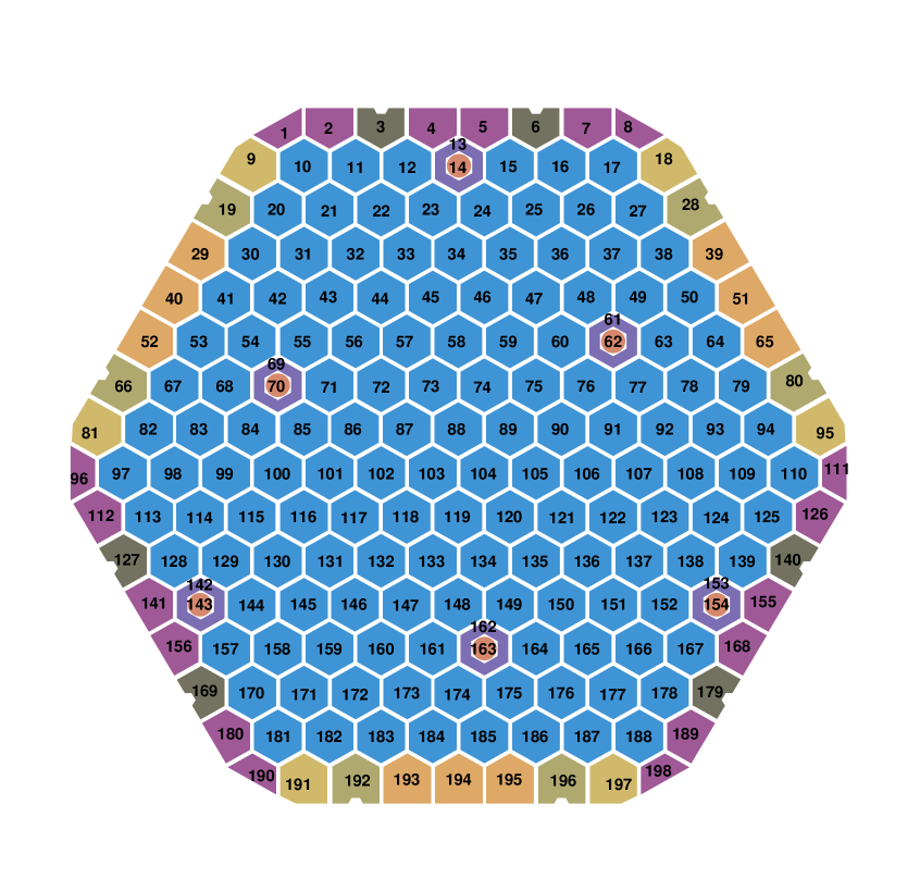
They are segmented into 198 pads, where full hexagonal pads are about , and or in active thickness.
LD sensors will be installed in regions of intermediate radiation levels inside the CE.
By contrast, regions with the highest radiation levels will be populated with HD sensors whose active thickness is .
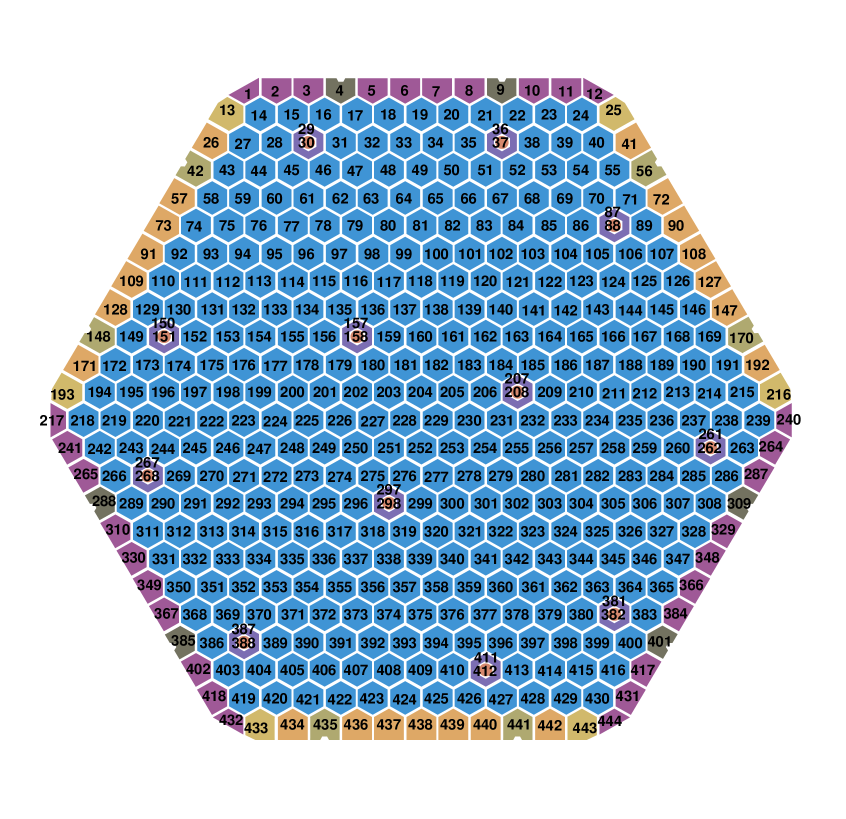
HD sensors are segmented into 444 pads (full hexagon pad size: ) and are produced by epitaxial growth.
As it is foreseen for the final design, p-stop structures were added to all the tested prototype silicon sensors in this work in order to limit the accumulation of electrons on the Si/SiO2 interface after exposure to high radiation levels which otherwise could form a conduction channel, effectively shorting adjacent pads.
Those structures were either bound to the single pads (individual p-stop) or shared between neighboring ones (common p-stop), representing two options under consideration for the CE.
In addition, the tested prototype sensors differed in their flatband voltage (pre-irradiation value of either or ).
Unless explicitly stated otherwise, all other production parameters, such as doping concentrations and the production process for the oxide material, were identical for all prototype sensors discussed in this paper.
Prior to irradiation, the sensors had been electrically qualified and proper functionality could be verified.
In particular, full depletion was achieved around for sensors, for sensors, and for sensors.
Moreover, per-pad leakage currents of the non-irradiated sensors did not exceed a few nA, and the total currents at room temperatures between 20– over the full sensor remained well below for (absolute) bias voltages up to .
In general, exposure of silicon sensors to radiation causes displacement damage to the silicon lattice which affects both the leakage currents and the depletion voltages.
While the bulk-dominated leakage current density increases proportionally with the fluence, the expected increase of the depletion voltage (for p-type sensors) is non-trivial and its quantification, like it is done e.g. in Refs. [13, 14], is beyond the scope of this work.
3 Irradiation at the Rhode Island Nuclear Science Center
3.1 Rhode Island Nuclear Reactor
The Rhode Island Nuclear Science Center (RINSC) houses a , light-water cooled, pool-type reactor in Narragansett, Rhode Island, USA.
Its core consists of fuel assemblies moderated with a combination of graphite and beryllium.
The fuel is plate type U3Si2, cladded with aluminum, enriched to less than 20 Uranium-235.
The reactor beam port was used as a sample delivery system because it was the only reactor access point large enough to fit a full-sized CE sensor.
The beam port in question had not previously been used for experiments, only for facility-related work.
A sketch of the beam port and a photo of its inside are shown in Figure 2.
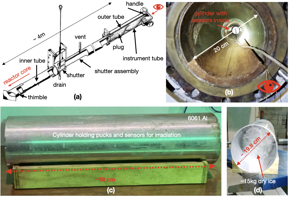
It measures about from its opening to the termination near to the reactor core, and it can accommodate samples with diameters of up to and with depths up to . A shutter assembly is located from the opening of the beam port, which must be raised to allow for the insertion of the samples and closed prior to the start of operations. A -long lead plug serves as a radiation shield that has to be inserted into the opening of the beam port prior to the start of the irradiation.
3.2 Irradiation of CE Silicon Sensor Prototypes
Given the constraints of the beam port system at RINSC, a dedicated sample delivery method had to be developed for irradiating CE silicon sensors. This new sample delivery allows for:
-
•
positioning sensors as close to the reactor core as possible;
-
•
protecting them from physical damage during the loading, irradiation, and unloading;
-
•
keeping the irradiated sensors at low temperatures during and after the irradiation;
-
•
monitoring the temperature of the samples inside the beam port.
Two compatible pieces of hardware were manufactured: a sensor container, referred to as a "hockey puck", and a sample delivery cylinder (see Figure 2). The former is used to protect, orient, and store the sensors during the irradiation while the latter is used to protect and locate the hockey puck inside the beam port. The cylinder is made from 6061 aluminum and has an outer(inner) diameter of (), allowing for a snug fit of the cylinder inside the beam port and a smooth insertion and removal of the hockey pucks. Three different hockey puck materials were considered (see Figure 3): oak, acrylic, and PEEK. They differ in their mechanical properties with respect to temperature and humidity fluctuations, in their activation, radiation hardness and overall cost. As a practical compromise between these factors, acrylic was found most suitable for irradiation up to fluences of , and PEEK material suitable for higher fluences. The usage of oak was eventually discarded because of its unfavorable tendency to absorb moisture.
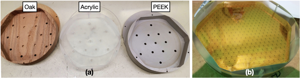
The puck base has an outer diameter of that allows for a smooth fit inside the cylinder.
The interior of the puck is milled out in the profile of the silicon sensors with an additional clearance of .
With these constraints the thinnest sections of the wall of the puck are slightly over thick.
Kapton™ foils were used to separate sensors in a stack such that no sensors were in direct contact with any metallic surfaces (cf. Figure 3).
In addition, antistatic foam was used for covering the top and bottom of the sensor-Kapton™ stack serving as a cushion against the walls inside the puck.
After preparation of the puck, the latter was inserted into the delivery cylinder.
In general, the silicon sensors should be kept at low temperatures during the irradiation in order to limit unwanted thermal annealing.
For this purpose, the rest of the delivery cylinder was filled with 15- of dry ice (Figure 2).
In order to monitor the temperature, PT1000 resistance temperature detectors (RTD) were inserted into the puck, at the front and back faces, to record the temperature throughout the irradiation for assessment of the expected sensor annealing during irradiation.
Representative temperature recordings from two irradiation rounds of different duration are shown in Figure 4.
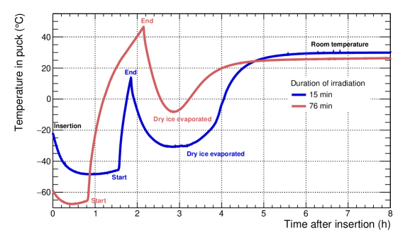
During irradiation, the temperature rose significantly, eventually reaching temperatures ranging from a few to . In fact, it was found that most of the dry ice sublimated. Only after shutdown of the reactor, the temperature decreased again. As a result, the annealing of the silicon sensors inside the beam port was not negligible. The corresponding annealing time at , cf. Ref. [13], varied between a few minutes to a few hundred minutes for all sensors irradiated at RINSC in 2020-21 up to . After in the beam port after irradiation, the cylinder’s activation levels had decayed sufficiently, it could be safely extracted, and transferred into a storage freezer.
3.3 Fluence Assessment
In addition to the sensors, mechanical packing material, and temperature sensors, each puck contained a number of reference samples for measuring the fluence achieved during an irradiation round. Two different objects were found appropriate for measuring the fluences during this campaign: silicon diodes, which were studied for usage in the D0 experiment [15], and ultrapure iron foils. The diodes were included inside the puck as close to the sensors as possible by encasing them in small plastic bags and taping them to the inside faces of the puck. By contrast, the iron foils were attached to the exterior of the cylinder for ease of removal and gamma spectroscopy measurements. The latter were performed at RINSC after irradiation for derivation of the integrated fluence. In addition, CV and IV measurements of the irradiated diodes were performed at Brown University to assess the depletion voltage, the associated dark current and ultimately the fluence assuming the literature value for the current-related leakage current rate of A/cm at [13]. The reference silicon diodes are most useful for the lower to medium range of the targeted fluences, where their depletion voltage was well within the measurement range (). For higher fluences, full depletion of the silicon diodes could not be reached, and the gamma ray spectra derived from the iron foils are considered more reliable. Table 1 in Appendix A shows the estimated actual fluences from those reference samples. In order to improve the accuracy of the fluence assessment, future irradiations will include iron foils inside the puck as well as additional silicon test structures.
4 Electrical Characterisation of Neutron-Irradiated Silicon Pad Sensors
The experimental setup and the electrical characterisation procedure of neutron-irradiated CE silicon pad sensors are presented in this section. The following paragraphs describe two similar setups installed at CERN and Texas Tech University, which were used to obtain the results reported in this paper. Since the majority of the results are based on the CERN setup, its specifics are elaborated in the following.
4.1 ARRAY- and Cold-Chuck Based Setup at CERN
At CERN, the S200FA probe station produced by Wentworth Laboratories Ltd. was used for the electrical characterisation of neutron-irradiated silicon pad sensors. Its chuck (Systems att, C200-40 model) is temperature-controlled down to .
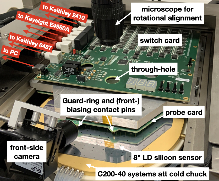
Apart from a Keithley 2410 power supply, a Keithley 6487 picoammeter, and a Keysight E4980A LCR-meter, all relevant components were installed inside the probe station, see Figure 5.
The silicon sensors were first placed on the chuck and then connected to the probe- and switch-card based ARRAY system that is described in detail in Ref. [11].
The contact between the probe card and the pads was realised with spring-loaded pins.
Through-holes in the cards and the probe station’s microscope enable sufficient sensor-to-probe card alignment.
Also, the sensor’s grounded guard ring was accessible via a dedicated contact pad and could be connected with dedicated pins on the probe card.
The high voltage from the power supply was provided to the chuck and with it to the sensor’s backside.
Two probe cards specific for the LD and HD sensor layouts have been designed and manufactured.
The switch card was operated with a bias resistance (R) of and a high voltage resistance (R) of , see [11] (Figure 9).
In this configuration, the ARRAY system is designed to safely withstand total leakage currents up to and per-pad currents up to .
Since these limits would have been exceeded by a few orders of magnitude at room temperature, cooling the neutron-irradiated sensors down to hereby reducing the leakage current by almost three orders of magnitude with respect to room temperature was imperative.
The spatial variation of the C200-40 chuck temperature profile at this temperature amounts to , cf. Appendix B, whereas fluctuations with time were found to be negligible.
For the purpose of preventing the formation of ice, the probe station was continuously flushed with dry air.
With total currents at the order of , the voltage drop at R for the testing of neutron-irradiated sensors corresponded to a few volts and was corrected for.
Per-pad leakage currents were measured with the picoammeter, whereas total currents were measured directly with the power supply.
The LCR meter was operated at a frequency (f) of for the inference of the per-pad impedance.
This particular frequency was chosen to minimise the error associated to the capacitance that is derived from it [11].
4.2 Characterisation Procedure
After connecting the sensor to the probecard, per-pad leakage currents as a function of the bias voltage for all pads on a given sensor were measured (IV).
This was followed by a per-pad capacitance vs. bias voltage assessment (CV).
After each iteration over all pads at a fixed bias voltage, voltages were incremented in varying steps between 50- up to , whereby the exact choice depended on the measurement type (IV/CV) and on the thickness of the sensor.
Although not applicable for the results shown in this work, it should be noted that a given measurement sequence was aborted if the total leakage current exceeded .
Similarly, individual pads whose leakage currents exceeded were not measured any further and in particular were excluded from the subsequent CV.
These compliance limits prohibited large voltage drops inside the test circuitry, minimising the risk of damage to the ARRAY system.
The entire characterisation sequence was fully automatised as a LabVIEW-based program (HexDAQ version 1.5.1 [16]).
Including voltage ramps and settling times, the IV(CV) measurements of low-density sensors in this work took about (), whereby the duration is proportional to the number of voltage steps (10-15 here).
The duration was about twice as long for high-density sensors due to the higher number of pads.
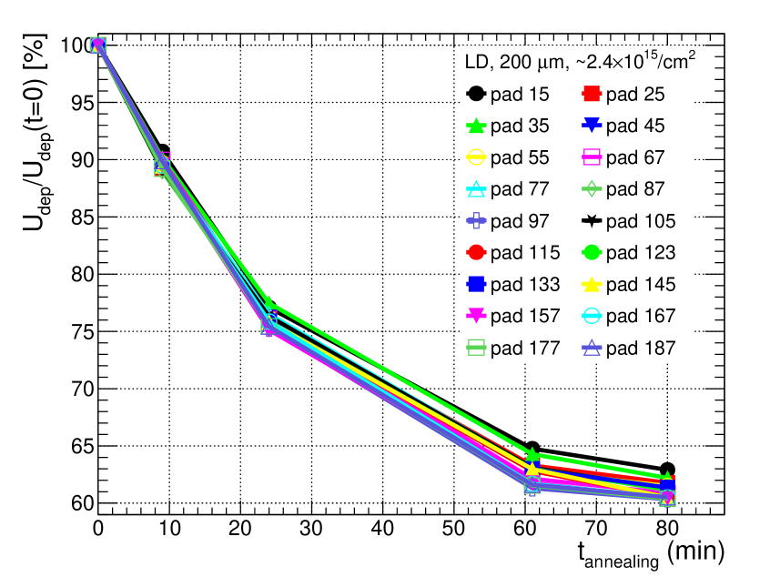
In order to quantify the potential performance benefit via annealing, silicon sensors were warmed up to inside the probe station.
After a total of at this temperature 111Corresponding to about three years at ., the sensor’s depletion voltage is expected to be minimal [17] and the studied sensors were cooled again to .
IV and CV characterisations were conducted before and after additional annealing.
5 Results
The results of the electrical characterisation of the neutron-irradiated CE silicon pad sensor prototypes are presented in this section. Section 5.1 focuses on the discussion of leakage currents (IV) whereas Section 5.2 addresses the capacitance (CV) and depletion voltage assessments. Section 5.3 offers a discussion on the drawn conclusion.
5.1 Leakage Current
The total leakage current, interpreted as the dark current of a full silicon sensor, is defined as the current flowing through the high-voltage resistor R (cf. Figure 2 in [11]).
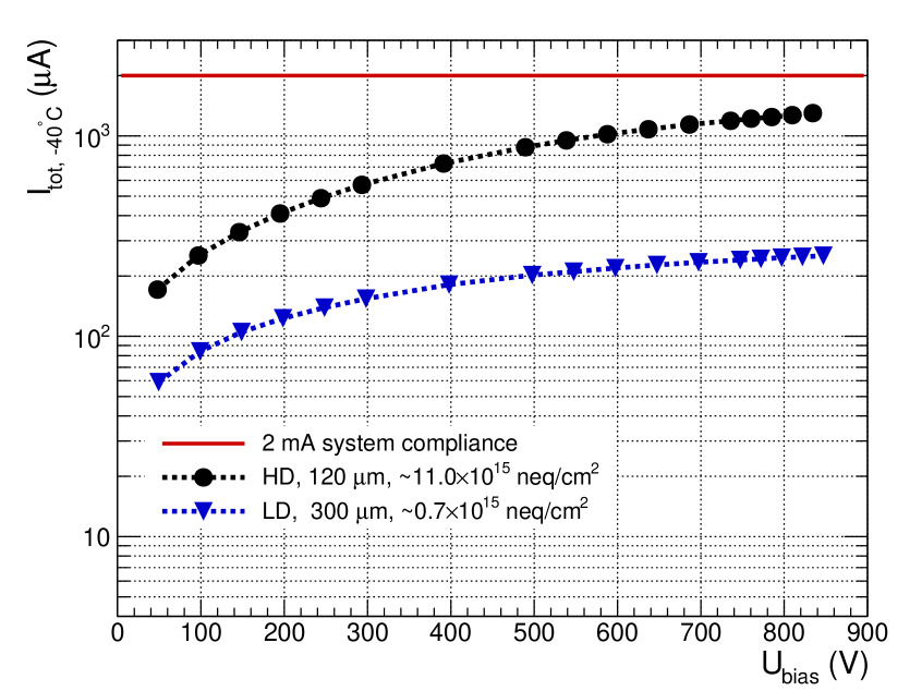
As it is shown for two prototype sensors in Figure 6(a), the total leakage current did not break down and stayed well below the ARRAY system’s compliance of for the irradiated sensors discussed in this paper.
Irreversible discharges are undesired but occurred for a handful of sensors where the total leakage current suddenly increased and exceeded the limitation.
One half of those instances could be traced back to mechanical damages, e.g. induced during the transport or sensor handling, and the other half hinted at the presence of a minor flaw in the CE silicon sensor design.
The latter ultimately lead to a design modification with which the risk of discharges in the future should be minimised222More than 50 prototype sensors with the improved design have been characterized with voltages up to in the meantime. None have shown discharges thus far..
Results of the affected sensors are not discussed further in this paper.
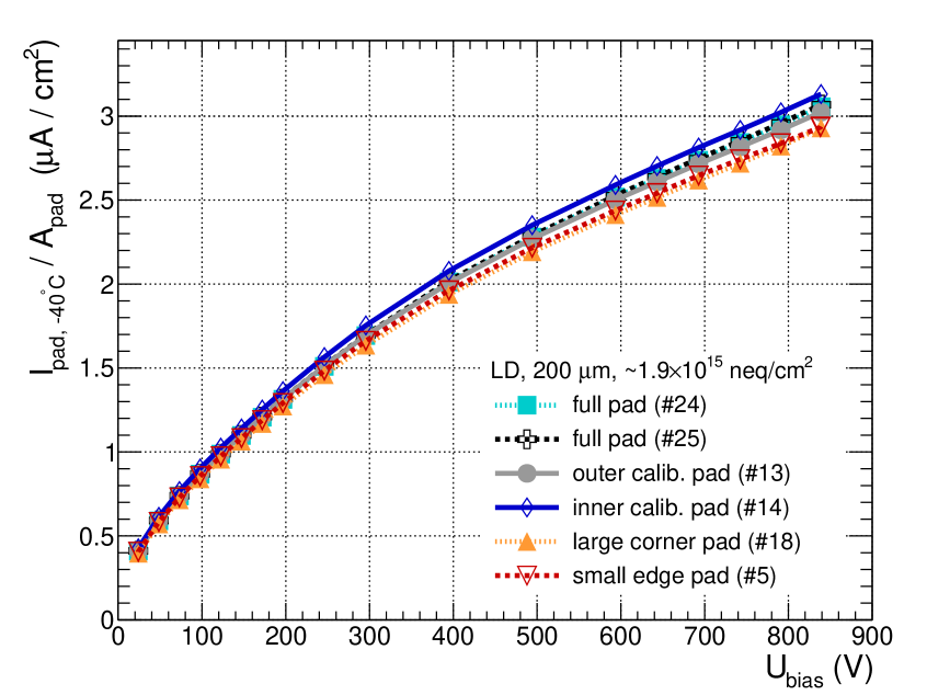
Figure 6(b) shows the per-pad leakage current as a function of the effective bias voltage for adjacent pads of various sizes on a low density sensor irradiated up to .
The data demonstrate that, in good approximation, the leakage current of a pad scales with its volume.
The relative increase from to remains well below meeting the vendor specifications.
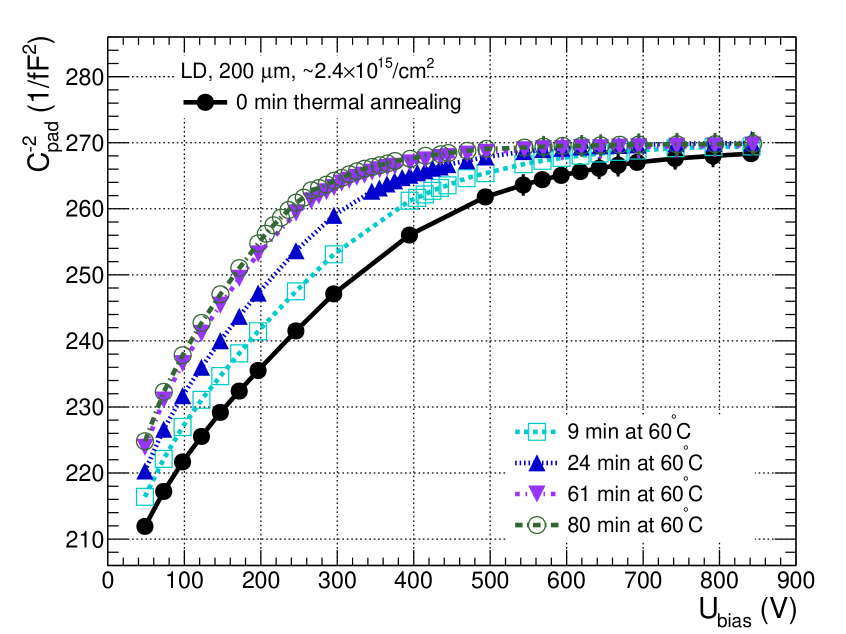
The IV curves after different annealing times are shown for a representative pad in Figure 7(a).
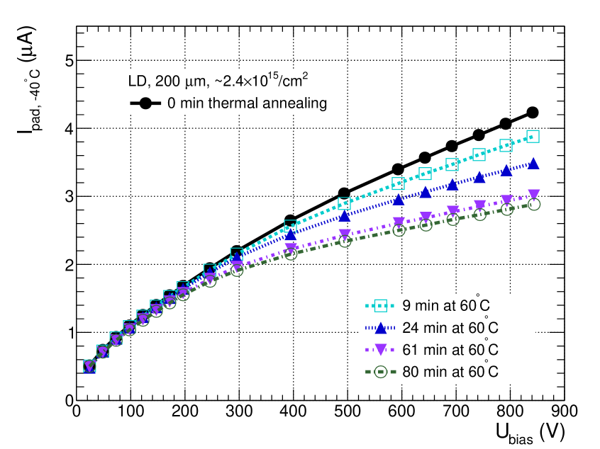
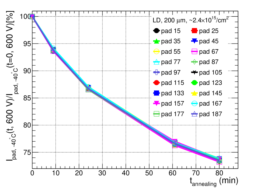
For bias voltages beyond full depletion, per-pad leakage currents at are reduced systematically by after at , cf. Figure 7(b).
Given the simultaneous reduction in the depletion voltage, cf. Figure 10(b), leakage currents around full depletion are even further reduced.
The expected relationship between the per-pad leakage current density and the fluence was observed.
The proportionality for current densities at a bias voltage of , which is well above full depletion for all investigated sensors (except for the sensors irradiated to ), and extrapolated to is displayed in Figure 8.
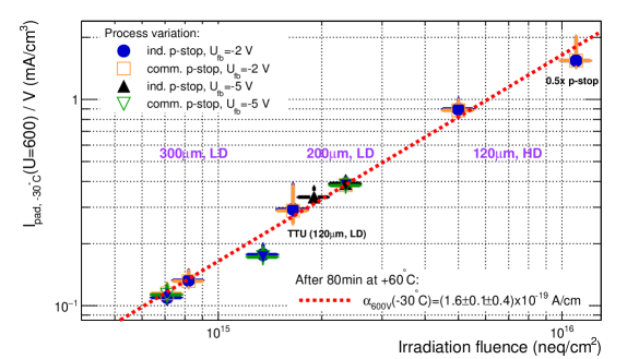
As expected [18], the current-related damage rate () is found to be independent on the tested material properties investigated in this work.
The numerical result for scaled to room temperature is A/cm.
The central value is about less than what is reported in Ref. [13].
A possible explanation could be a systematic overestimation of the fluence at the RINSC irradiation facility.
Follow-up studies in this regard are anticipated in the mid-term future.
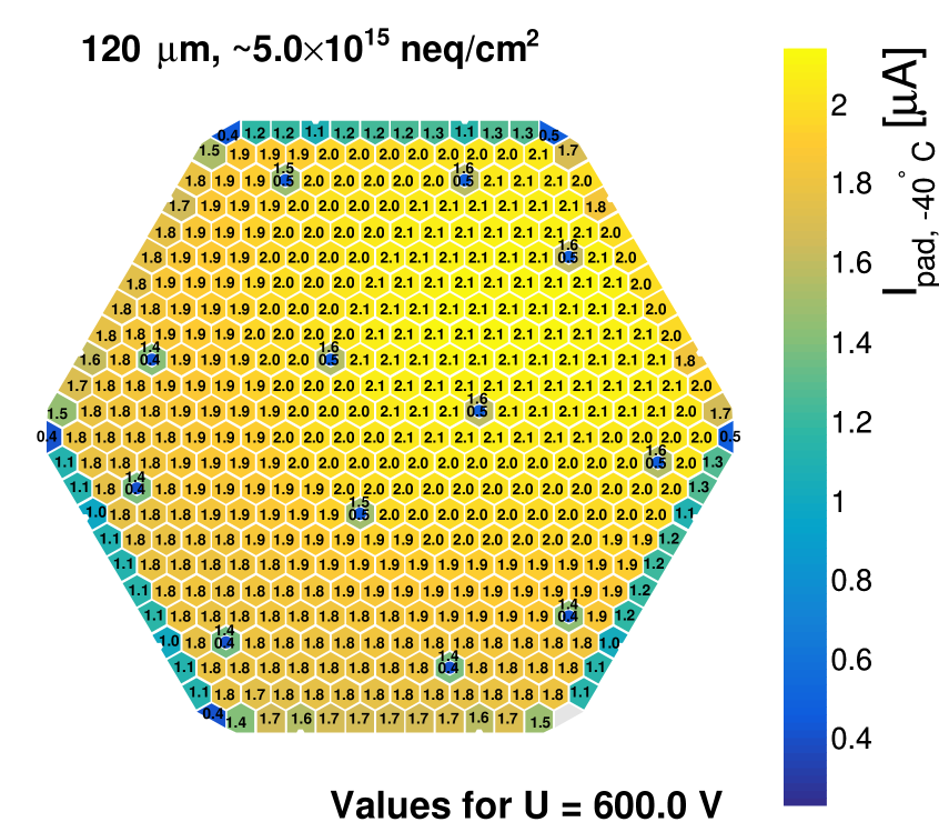
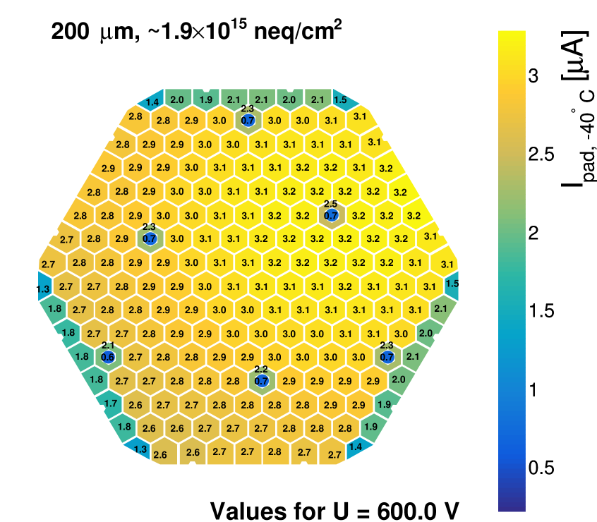
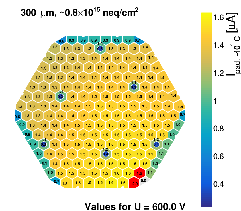
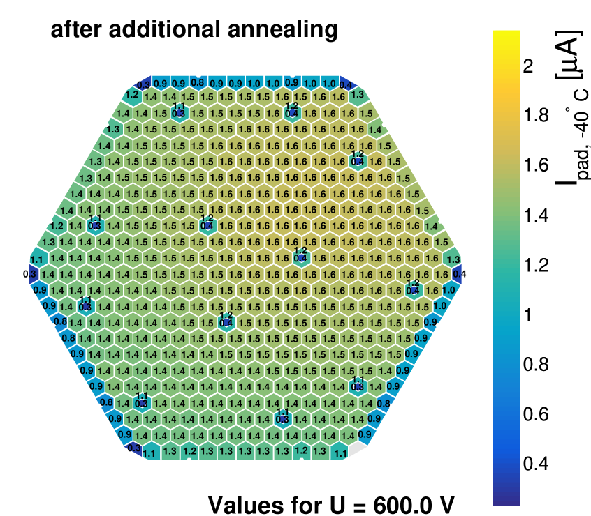
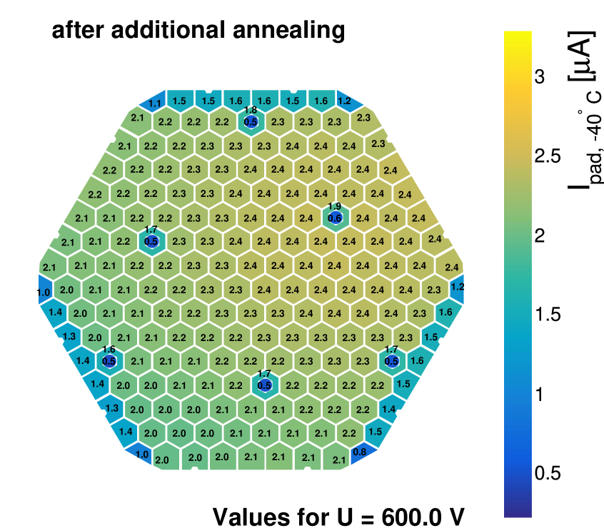
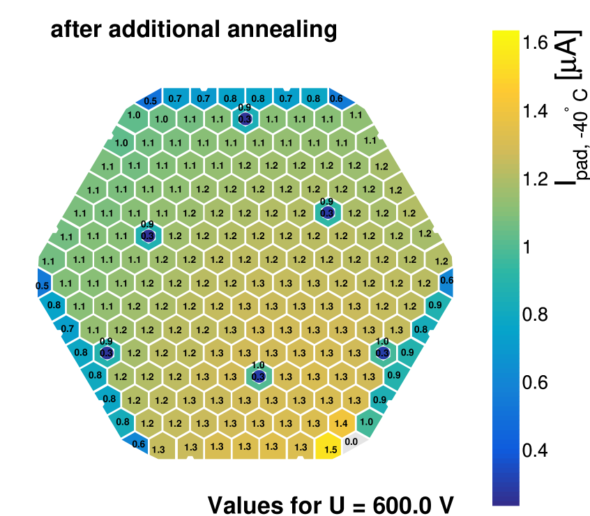
After correction for the chuck temperature non-uniformity, per-pad leakage current densities across a sensor at a fixed voltage still vary by .
The associated current profiles are present both before (cf. Figures 9(a), 9(b) and 9(c)) and after additional annealing (cf. Figures 9(d), 9(e) and 9(f)).
Furthermore, they are consistent between sensors that had been irradiated simultaneously in the same puck.
Among others, a plausible explanation for this observation could be the presence of a fluence profile within the beam port at RINSC that can be approximated as a Gaussian with a width of .
5.2 Capacitance and Depletion Voltage
The measured per-channel impedance is open-corrected by subtracting the impedance of the ARRAY system.
Subsequently, the sensor pad capacitance is computed assuming an underlying serial connection to the measurement circuitry.
Due to the finite mobility of the sensor defects, the frequency at which the impedance is measured may, in principle, have sizeable impact on the derived capacitance and on the depletion voltages, cf. Ref. [19].
The impedance measurement was conducted at .
Experimental follow-up indicated an impact of on the asymptotic capacitance and a reduction of the depletion voltage when decreasing to , which have no implication on the following discussion.
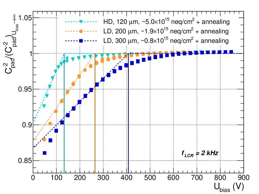
The depletion voltage for each pad is assessed from the saturation of its squared reciprocal capacitance () of a pad with respect to the bias voltage ().
It is defined as the intersection of a straight-line fitted to the rising part of the vs. curve with a line fitted to its plateau.
Prior to additional annealing, such a plateau could not always be reached within the tested bias voltage range, see for example the black line in Figure 10(a).
After additional annealing to at , the estimated depletion voltage has been reduced by about a third with respect to the case without annealing, cf. Figure 10(b).
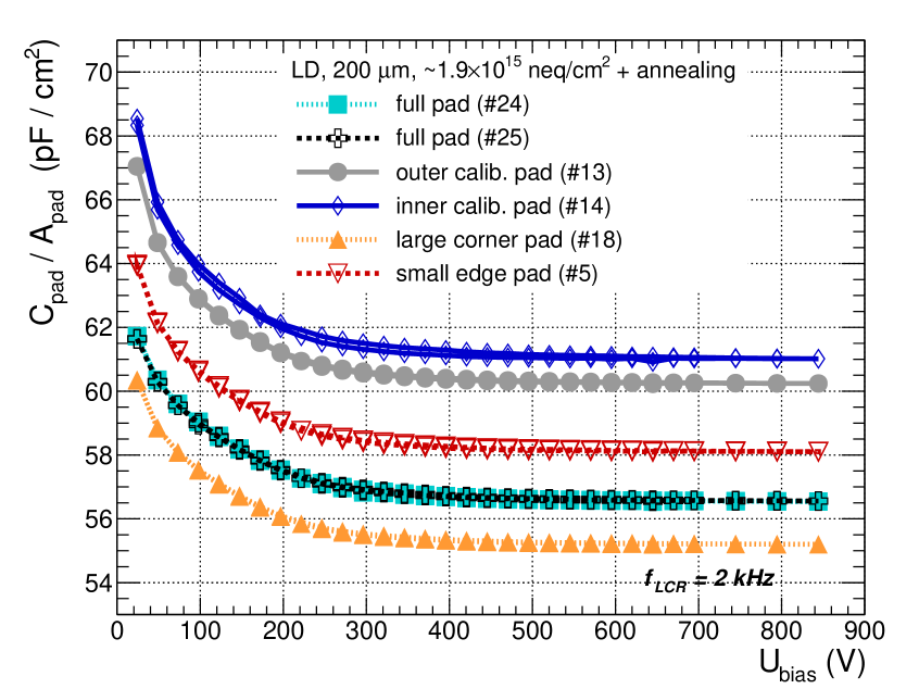
The per-pad capacitance after irradiation is found to scale well with the area of the pad, cf. Figure 11(a).
Deviations from this scaling amount to less than , suggesting a slight dependence of the inter-pad capacitances on the pad geometries.
Figure 11(b) illustrates that the estimated depletion voltages depend primarily on the associated thickness of the depleted zone.
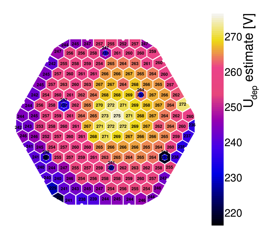
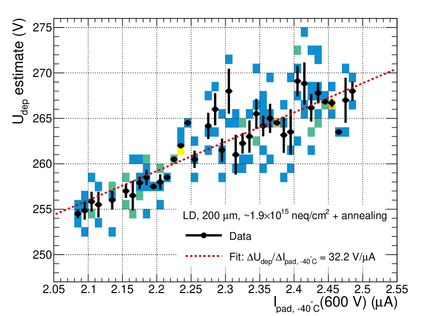
The estimated per-pad depletion voltage across the sensor is shown in Figure 12(a). Those estimates exhibit positive correlation with the leakage currents, taken as proxy for the fluence, cf. Figure 12(b). In fact, the obtained correlation coefficient from this analysis is positive for all tested sensors where full depletion could be reached. This can be interpreted as further evidence for the presence of a fluence profile inside the beam port during irradiation.
5.3 Discussion
The neutron irradiation induced leakage currents are consistent both qualitatively and quantitatively with previous RD on irradiated silicon sensors.
They are also found to be independent of the silicon fabrication process (flatband voltage, p-stop layout).
Furthermore, unchanged end-capacitances and reduced depletion voltages after beneficial annealing are qualitatively consistent with previous findings.
The findings presented in this paper with the first prototypes of CE silicon sensors, i.e. hexagonal sensors and fabricated with a new 8” process, irradiated to fluences corresponding to the end of lifetime of HL-LHC are in full support of the radiation-hardness of their general design.
By implication, RINSC could be qualified as a valid facility for neutron irradiation of 8” silicon sensors for the first time.
However, more accurate studies on the electrical sensor properties after neutron-irradiation would need to incorporate the systematic uncertainty on the effective annealing during irradiation, that is due to the temperature evolution and its potential lateral profile inside the reactor’s beam port.
Similarly, an accurate assessment of the actual fluence at each pad would have to address the neutron flux profile, for whose existence this work provides first evidence.
6 Conclusion
An essential component of the silicon sensors’ prototyping for the CMS highly granular endcap calorimeter upgrade (CE) is the experimental verification of the radiation hardness in terms of their electrical properties, i.e. leakage currents, capacitances and depletion voltages.
RINSC is one of the few locations world-wide that offers the infrastructure for the irradiation of large structures compatible with CE’s 8”-wide silicon pad sensors.
Given that parts of the necessary infrastructure have not been used in this experimental capacity, the irradiation was non-trivial and specific preparations had to be made.
After irradiation, the probe- and switch card-based ARRAY system [11] was used for the first time for the electrical characterisation of neutron-irradiated silicon sensors at CERN and at Texas Tech University.
In order to protect the test system from currents that would exceed its specifications, the neutron-irradiated sensors were cooled down to during the tests.
The preparation and execution of the neutron-irradiation at RINSC and the electrical characterisation of the irradiated sensors at cold temperatures using the ARRAY system was explained in this paper.
Evidence for specific properties of the RINSC irradiation facility such as a non-uniform flux profile across the 8” wafer and for non-negligible sensor annealing due to insufficient cooling during irradiation was reported.
For the planned CMS CE upgrade, the findings in this work are encouraging as they confirm the overall expected radiation hardness of the prototype silicon sensors.
In particular, their leakage current densities are found to scale proportionally with the fluence, independent of the properties of the tested production process variations.
It is reconfirmed that annealing the sensors up to at has beneficial impact on the electrical properties by lowering the dark current and the depletion voltages by .
Despite the tested sensors being prototypes, the insights from their characterisation can be considered representative for the final version.
Therefore, the results reported in this work may serve as reference for the expected electrical performance and degradation of CE’s silicon sensors towards the end of their lifetime at HL-LHC.
Acknowledgments
We thank the staff at the Rhode Island Nuclear Science Center for their support during the preparation and execution of the neutron irradiation of the CE silicon pad sensor prototypes. The EP-DT and the former EP-LCD group at CERN have developed essential infrastructure, such as the ARRAY system including the associated data acquisition software, and have co-financed the acquisition of the utilised cold-chuck probe station at CERN. Without their input, this RD milestone towards the realisation of this novel calorimeter would not have been possible. We are thankful for the technical and administrative support at CERN and at other CMS institutes and thank the staffs for their contributions to the success of the CMS effort. We acknowledge the enduring support provided by the following funding agencies and laboratories: BMBWF and FWF (Austria); CERN; CAS, MoST, and NSFC (China); MSES and CSF (Croatia); CEA, CNRS/IN2P3 and P2IO LabEx (ANR- 10-LABX-0038) (France); SRNSF (Georgia); BMBF, DFG, and HGF (Germany); GSRT (Greece); DAE and DST (India); MES (Latvia); MOE and UM (Malaysia); MOS (Montenegro); PAEC (Pakistan); FCT (Portugal); JINR (Dubna); MON, RosAtom, RAS, RFBR, and NRC KI (Russia); MoST (Taipei); ThEP Center, IPST, STAR, and NSTDA (Thailand); TUBITAK and TENMAK (Turkey); STFC (United Kingdom); and DOE (USA).
Appendix A Irradiation Rounds and Fluences
See Table 1.
| Date | No. sensors | Thickness | Duration | Fluence () | Reference |
|---|---|---|---|---|---|
| 26 Aug 20 | 4 | 300m | 7.1 | Si diodes | |
| 20 Oct 20 | 4 | 120m | 110.0 | Fe foils | |
| 28 Jan 21 | 4 | 200m | 23.5 | Si diodes | |
| 11 Feb 21 | 4 | 120m | 16.5 | Si diodes | |
| 01 March 21 | 4 | 300m | 13.5 | Si diodes | |
| 11 March 21 | 4 | 120m | 50.0 | Fe foils | |
| 15 April 21 | 4 | 300m | 8.2 | Si diodes | |
| 06 May 21 | 2 | 200m | 19.0 | Si diodes |
Appendix B Temperature Uniformity of the Systems att C200-40 Cold Chuck
The leakage current in silicon devices dependends on the temperature. For the investigated sensors in this work, the current is mainly generated in the bulk for which the temperature () and current () are related by Equation B.1 [21], where is the effective gap energy and denotes the Boltzmann constant.
| (B.1) |
The validity of this temperature scaling law applied for the CE silicon pad sensors in the relevant temperature range has been verified and is illustrated in Figure 13.
Notably, a change by impacts the current by more than 10. Variations of the temperature across the actively cooled-down chuck, and with it across the sensor, may mimic neutron fluence profiles as in Figure 9. Thus, they should be identified and corrected for. In this work, the temperature non-uniformity of the cold chuck at CERN (C200-40 model produced by Systems att) could be estimated from leakage current data of neutron-irradiated sensors. By comparing per-pad currents () at a fixed bias voltage between the symmetry locations , , , described below, temperature differences can be calculated according to Equation B.2. For this purpose, one of the neutron-irradiated low-density sensors was characterised three times at , , and rotation. The precision in repeating the sensor placement on the chuck can be neglected with respect to the size of the pads.
| (B.2) |
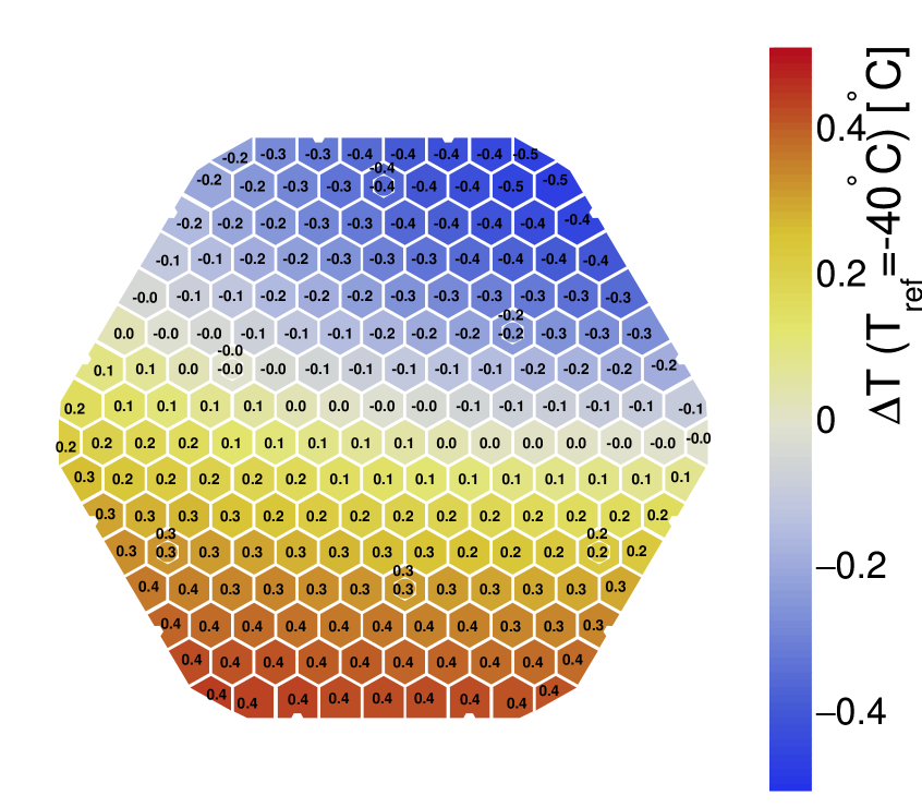
Figure 14(a) shows the hereby computed chuck temperature differences. The determined variation is consistent with the non-uniformity as specified by the chuck producer. Assuming a reference temperature of , a two-dimensional gaussian parameterisation bound to is fitted to reproduce the temperature differences . The result of the fit is shown in Figure 14(b).
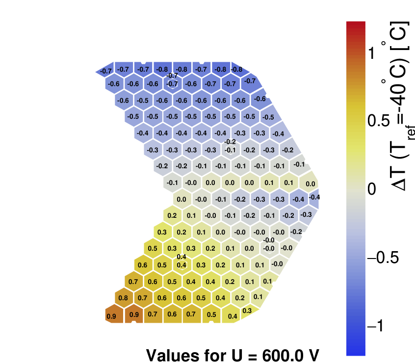
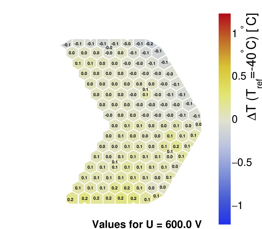
The hereby constructed map of chuck temperature differences is input to correct the measured per-pad leakage currents using Equation B.1. As a closure check, the re-application of Equation B.2 on the temperature-corrected dataset demonstrates the applicability of this particular chuck temperature model as shown in Figure 14(c).
References
- [1] L. Evans and P. Bryant. LHC machine. JINST, 3:S08001, 2008.
- [2] B. Alonso et al. High-Luminosity Large Hadron Collider (HL-LHC): Technical design report. CERN, 2020.
- [3] CMS Collaboration. The CMS Experiment at the CERN LHC. JINST, 3:S08004, 2008.
- [4] CMS Collaboration. The Phase-2 Upgrade of the CMS Endcap Calorimeter. CERN-LHCC-2017-023, 2017.
- [5] N. Akchurin et al. First beam tests of prototype silicon modules for the CMS High Granularity Endcap Calorimeter. JINST, 13:P10023, 2018.
- [6] B. Acar et al. The DAQ system of the 12,000 channel CMS high granularity calorimeter prototype. JINST, 16(04):T04001, 2021.
- [7] B. Acar et al. Construction and commissioning of CMS CE prototype silicon modules. JINST, 16(04):T04002, 2021.
- [8] B. Acar et al. Response of a CMS HGCAL silicon-pad electromagnetic calorimeter prototype to 20-300 GeV positrons, 2021.
- [9] E. Currás et al. Radiation hardness study of Silicon Detectors for the CMS High Granularity Calorimeter (HGCAL). JINST, 12(02):C02056, 2017.
- [10] N. Akchurin et al. Charge collection and electrical characterization of neutron irradiated silicon pad detectors for the CMS High Granularity Calorimeter. JINST, 15(09):P09031–P09031, 2020.
- [11] E. Brondolin et al. ARRAY: An open source, modular and probe-card based system with integrated switching matrix for characterisation of large area silicon pad sensors. NIM A, 940:168–173, 2019.
- [12] W. Adam et al. P-Type Silicon Strip Sensors for the new CMS Tracker at HL-LHC. JINST, 12(06):P06018, 2017.
- [13] M. Moll. Displacement Damage in Silicon Detectors for High Energy Physics. IEEE Transactions on Nuclear Science, 65(8):1561–1582, 2018.
- [14] G. Lindström. Radiation damage in silicon detectors. NIM A, 512(1):30–43, 2003.
- [15] A. Bean et al. Studies on the Radiation Damage to Silicon Detectors For Use in the D0 Run2b Experiment. D0 Note 3958, 2002.
- [16] A. Maier et al. HexDAQ. Version: v1.5.1. Last access: 07 January 2022.
- [17] M. Moll. Radiation damage in silicon particle detectors: Microscopic defects and macroscopic properties. PhD thesis, Universität Hamburg, 1999.
- [18] M. Moll, E. Fretwurst and G. Lindström. Leakage current of hadron irradiated silicon detectors – material dependence. NIM A, 426(1):87–93, 1999.
- [19] Z. Li and H.W. Kraner. Studies of frequency dependent C-V characteristics of neutron irradiated p/sup +/-n silicon detectors. IEEE Transactions on Nuclear Science, 38(2):244–250, 1991.
- [20] V. Radulovic et al. Large Object Irradiation Facility In The Tangential Channel Of The JSI TRIGA Reactor. 2017.
- [21] A. Chilingarov. Temperature dependence of the current generated in Si bulk. JINST, 8(10):P10003, 2013.