Further author information: (Send correspondence to Benjamin G. Westbrook)
E-mail: bwestbrook@berkeley.edu, Telephone: 1 415 308 6193
del⟨⟩
Development of the Low Frequency Telescope Focal Plane Detector Modules for LiteBIRD
Abstract
LiteBIRD is a JAXA-led strategic large-class satellite mission designed to measure the polarization of the cosmic microwave background and Galactic foregrounds from 34 to 448 GHz across the entire sky from L2 in the late 2020s. The scientific payload includes three telescopes which are called the low-, mid-, and high-frequency telescopes each with their own receiver that covers a portion of the mission’s frequency range. The low frequency telescope will map synchrotron radiation from the Galactic foreground and the cosmic microwave background. We discuss the design, fabrication, and characterization of the low-frequency focal plane modules for low-frequency telescope, which has a total bandwidth ranging from 34 to 161 GHz. There will be a total of 4 different pixel types with 8 overlapping bands to cover the full frequency range. These modules are housed in a single low-frequency focal plane unit which provides thermal isolation, mechanical support, and radiative baffling for the detectors. The module design implements multi-chroic lenslet-coupled sinuous antenna arrays coupled to transition edge sensor bolometers read out with frequency-domain mulitplexing. While this technology has strong heritage in ground-based cosmic microwave background experiments, the broad frequency coverage, low optical loading conditions, and the high cosmic ray background of the space environment require further development of this technology to be suitable for LiteBIRD. In these proceedings, we discuss the optical and bolometeric characterization of a triplexing prototype pixel with bands centered on 78, 100, and 140 GHz.
keywords:
SPIE, Cosmic Microwave Background, Detectors, Space-Mission, Polarization, Inflation, Cosmic Foregrounds, Satellite, LiteBIRD1 Introduction
LiteBIRD is a JAXA-led strategic Large-Class satellite mission that will map the polarization of the Cosmic Microwave Background (CMB) and cosmic foreground over the entire sky with an angular resolution appropriate to cover the multipole range . The payload consists of three telescopes called the Low-Frequency Telescope (LFT), Mid-Frequency Telescope (MFT), and High-Frequency Telescope (HFT) each of which has a corresponding Focal Plane Unit (FPU). It is the primary responsibility of the US team to deliver the flight model (FM) FPU s for the mission. LiteBIRD will deploy a total of 15 detector bands ranging from 34 to 448 GHz which are distributed across the Low-Frequency Focal Plane Unit (LF-FPU), Mid-Frequency Focal Plane Unit (MF-FPU), and High-Frequency Focal Plane Unit (HF-FPU). An overview of LiteBIRD can be found in the journal of the Progress of Theoretical and Experimental Physics (PTEP) [1, 2].
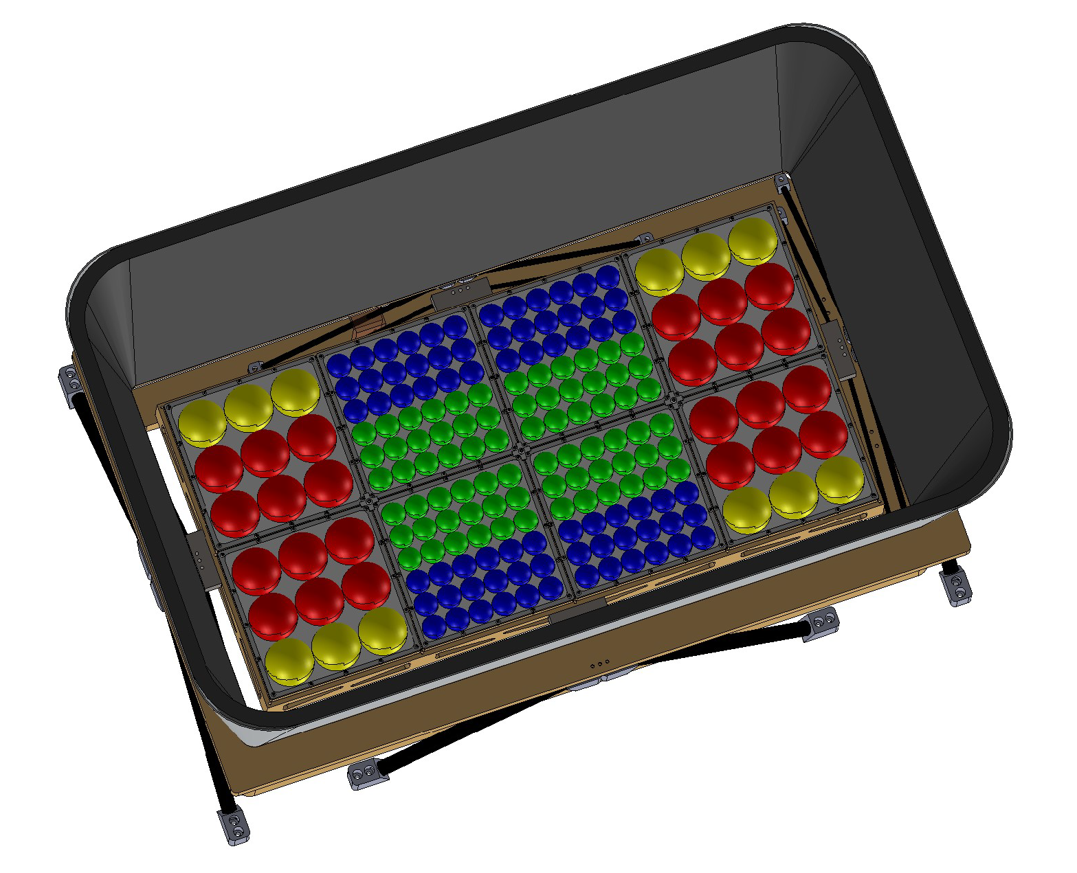
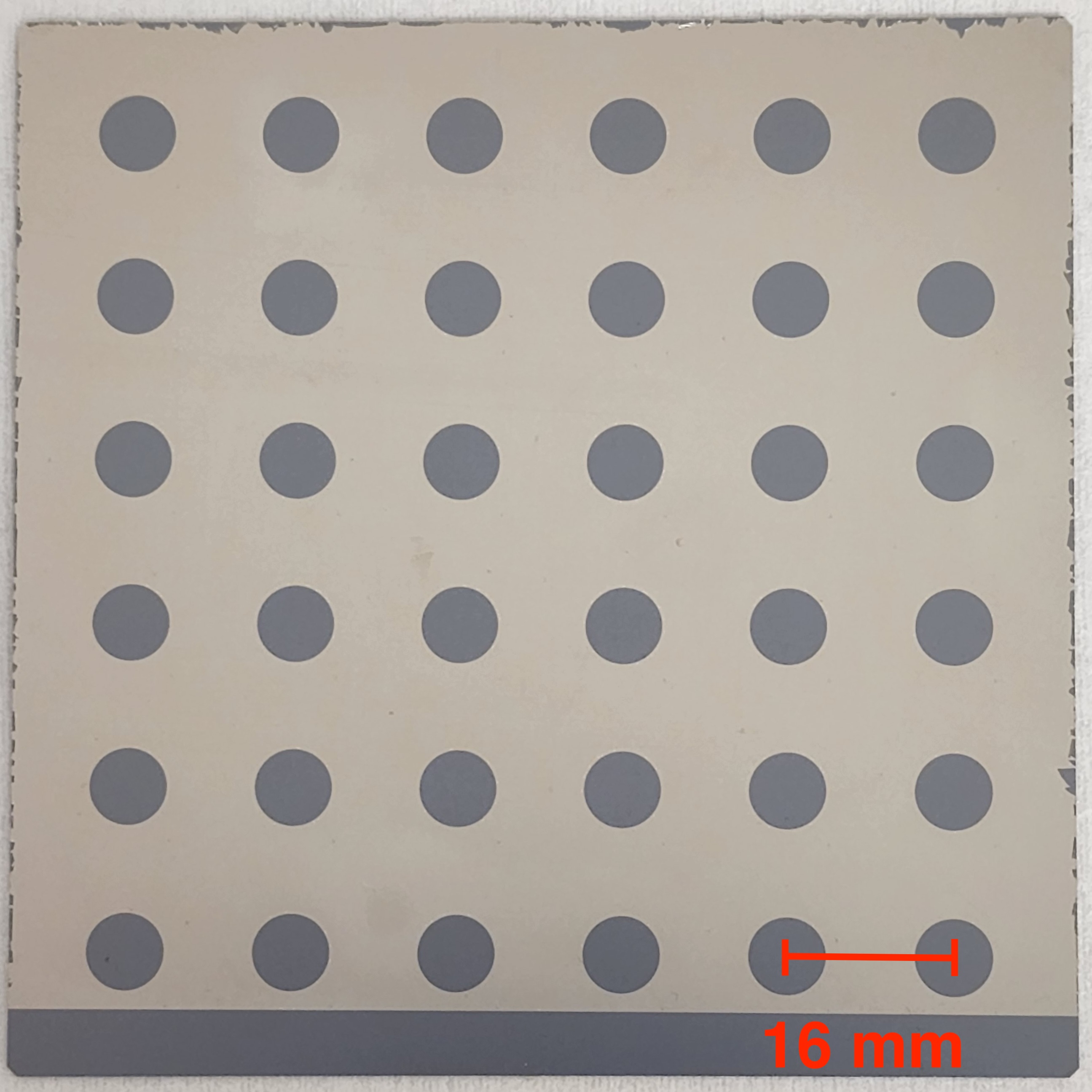
The LF-FPU holds eight square 140 mm x 140 mm tiles with four distinct pixel types and two distinct Focal Plane Module (FPM) types with a pixel pitch of 32 mm for the lowest frequency pixels and 16 mm for the highest frequency pixels. The LF-FPU has a frequency coverage of 34 to 161 GHz making it sensitive to both synchrotron radiation and the CMB. These proceedings will discuss the development of the FPMs for the LF-FPU, including the optical interfaces to the telescope, the coupling to the digital frequency-domain multiplexing (DfMux) readout, implementation of cosmic ray mitigation, and the development of one of the triplexing pixels in the LFT.
The LF-FPU is being developed at the University of California, Berkeley (UC Berkeley) Marvell Nanofabrication Laboratory (MNL) in close collaboration with researchers at Boulder Microfabrication Facility (BMF) at the National Institute of Standards and Technologies (NIST) [3]. Both institutions have extensive heritage in fabricating Transition-Edge Sensor (TES) bolometer arrays for studies of the polarization of the CMB for both ground-based and balloon-borne experiments making them especially suitable for LiteBIRD. The MNL is a 10,000 square foot class 100 clean room that has rich heritage of fabricating detectors for CMB experiments including: APEX-SZ, SPT-SZ, EBEX, POLARBEAR-1, Simons Array (SA), and Simons Observatory (SO) [4, 5, 6, 7, 8]. The High Energy Accelerator Research Organization in Tsukuba, Japan (KEK) will provide the LF-FPU to the mission while the US will be in charge of developing and testing the FPMs for the mission.
In addition to the work reported in these proceedings, there are other relevant developments for LiteBIRD reported at this conference. More information on development of LFT and MFT detector arrays at NIST and University of Colorado, Boulder (CU) is in SPIE 2022 proceedings by Jaehnig. [3]. One can find information on the susceptibility of LiteBIRD TESs to magnetic fields in SPIE 2022 proceedings by Ghigna[9]. One can also find more details on Cryogenic Readout Electronics (CRE) development for LiteBIRD in SPIE 2022 proceedings by Russell[10].
2 Coupling Design
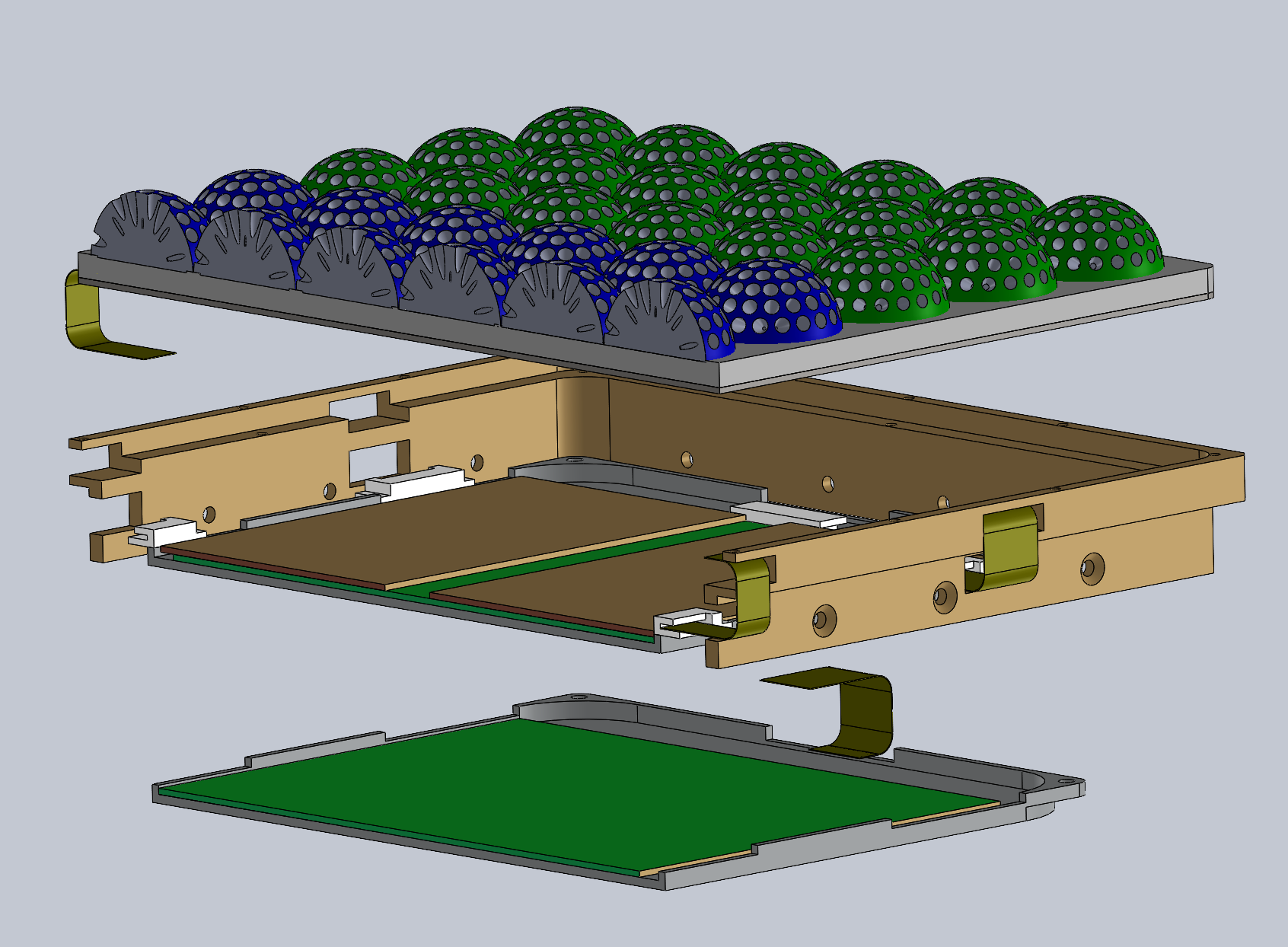
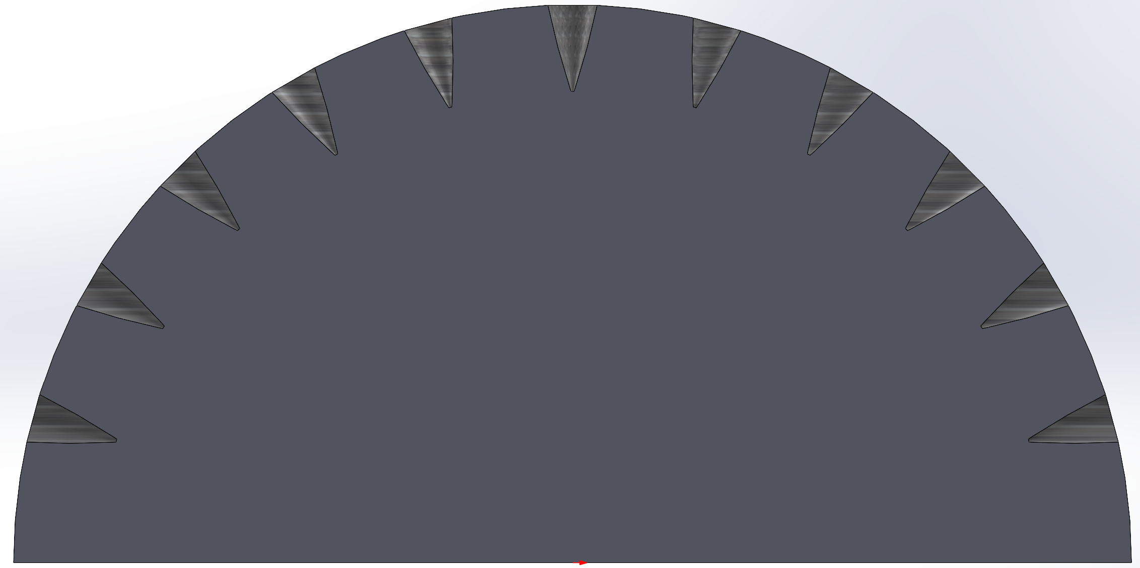
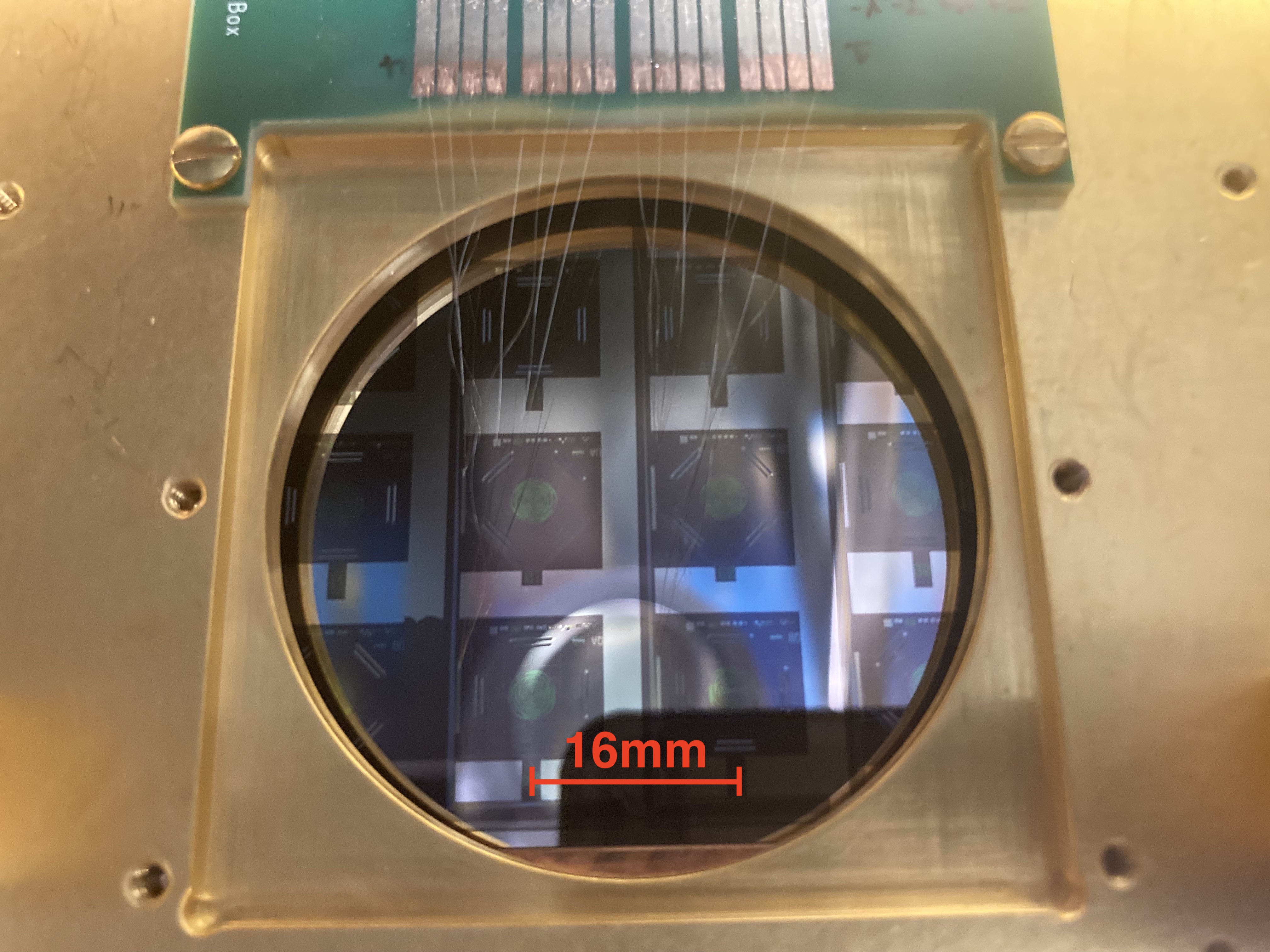
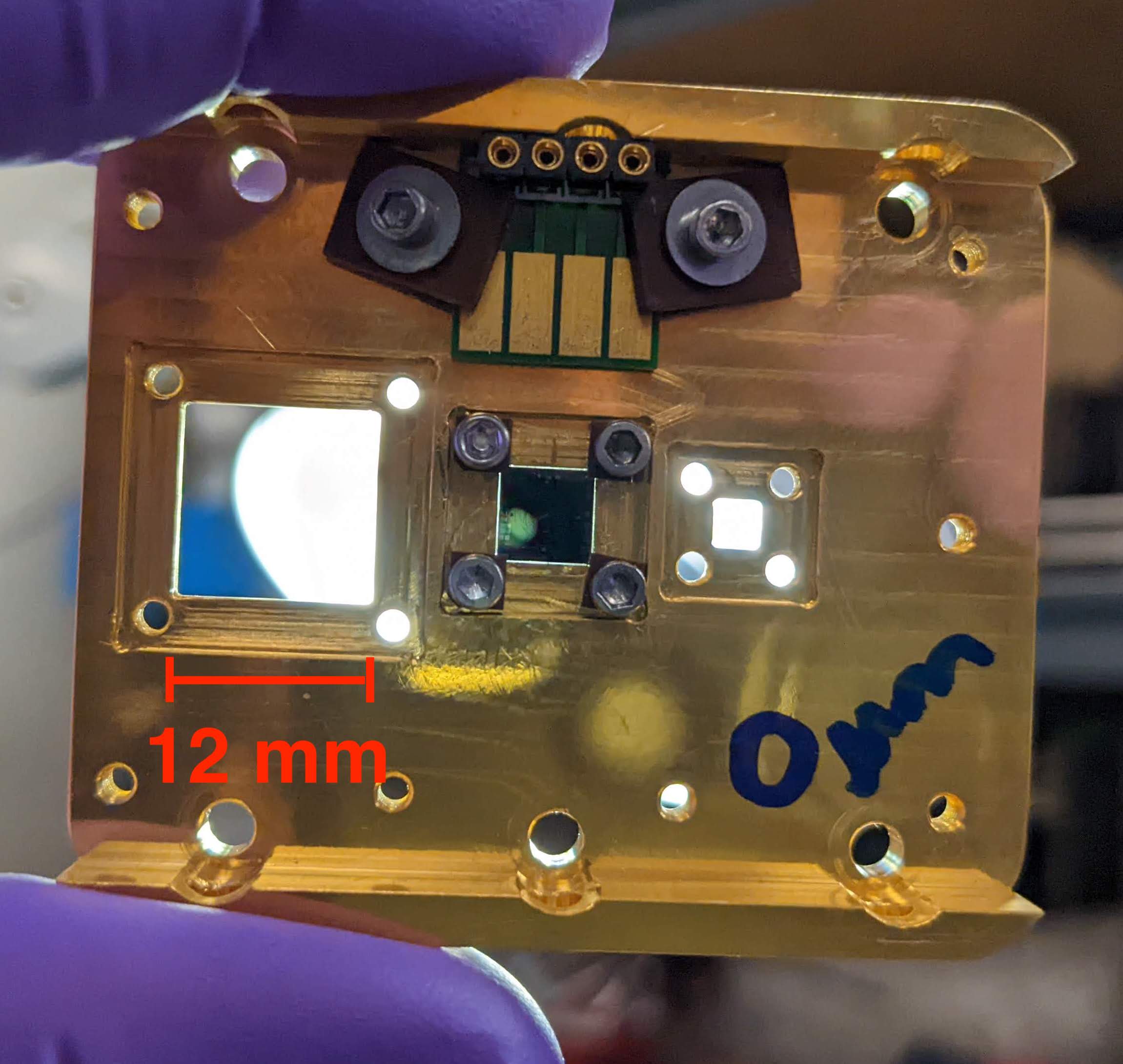
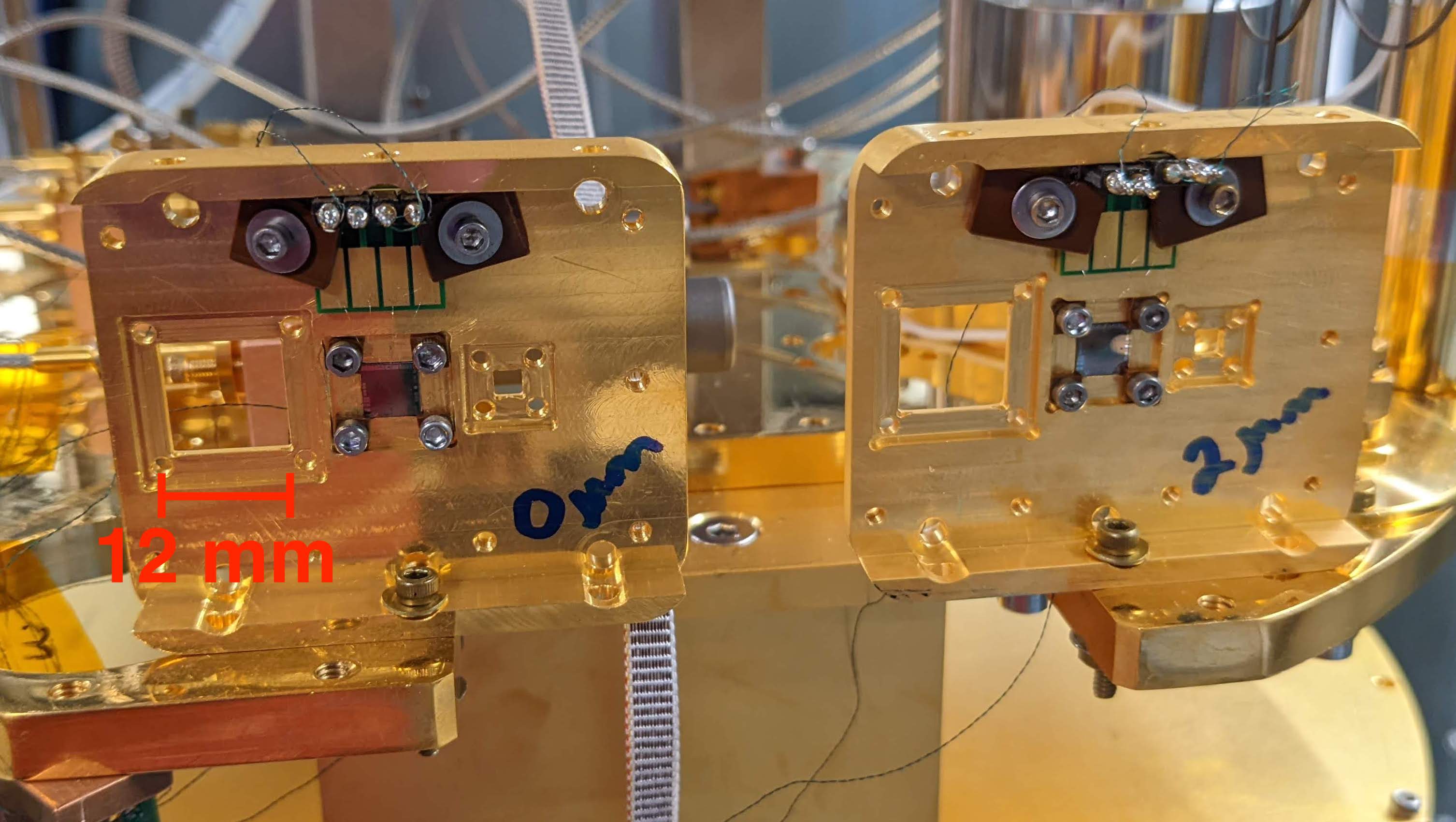
These proceedings will focus on the elements of the detection chain once the light from the telescope is focused the detectors in the focal plane. The LF-FPU, will tile FPMs into a four by two array as shown in the left hand side of Figure 1. A full description of detection chain can be found in PTEP [1]. There are three major components in the FPMs; the lenslets which couple the antenna to the telescope, the detectors which filter and sense the incoming photons, and the DfMux readout electronics housed on the back (non-sky) side of the focal plane. The major elements are shown in the right hand side of Figure 1. This technology is able to reach the instantaneous sensitivity required by the LiteBIRD mission and is a mature technology with well-established use in ground-based and sub-orbital CMB experiments [6, 11, 12].
2.1 Lenslets
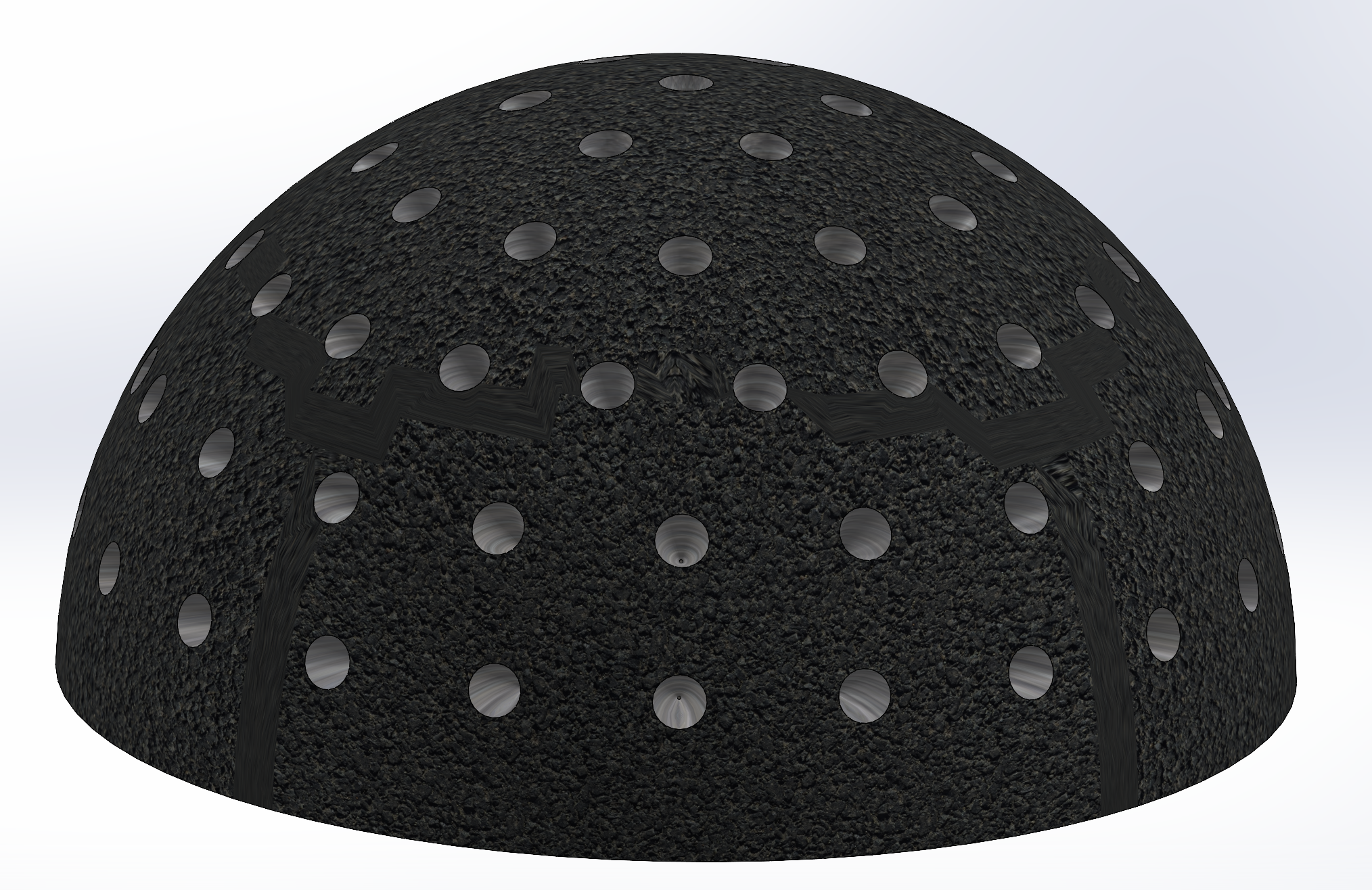
A ‘lenslet’ is a contact lens (usually silicon or alumina) concentrically aligned to a planar antenna to increase the forward gain of said antenna with minimal absorption loss [13, 14]. In the LiteBIRD design, the lenslets are individually fabricated silicon hemispheres which are bonded to a silicon extension wafer. The hemisphere combined with this extension wafer approximates an ellipse to optimize the forward gain. This technology requires AR coating or surface to minimize the loss at the vacuum-dieletric interface [15]. LiteBIRD will implement a Metamaterial Anti-Reflection Surface (MARS) on all of the lenslets in the LFT and MFT. The beam properties of the detectors are primarily determined by the diameter and symmetry of the lenslet and its AR surface rather than the antenna itself. A summary of pixel properties with their beam sizes is given in Table 1.
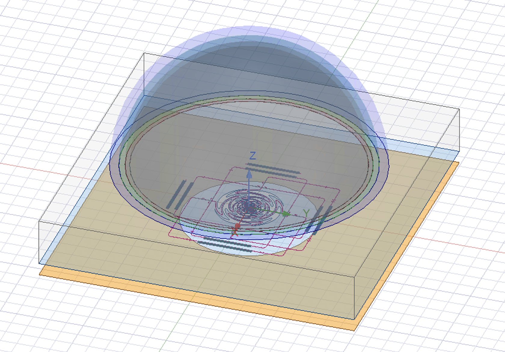
The LHS of Figure 2 shows a High Frequency Simulation Software (HFSS) simulation setup of a lenslet placed over a LF-4 pixel. In this simulation the AR coating is simulated as a traditional three layer quarter-lambda AR coating. In the case of LiteBIRD the lenslet will appear as they do in the RHS of 2.
2.1.1 Metamaterial Anti-Reflection Surfaces (MARS)
Metamaterials are an attractive option for LiteBIRD as they can be tuned to cover the entire frequency range of the LFT and MFT and do not rely on epoxies or other glues to adhere to the silicon lenslets, which can be prone to differential thermal contractions. The metamaterial creates an effective index of refraction by strategically removing silicon from the substrate to create a sub-wavelength structure in the silicon. The shape and size of the structure determines how the index of refraction will change as function of depth in the hole itself as described in Farias 2022 [15]. An example Computer Automated Design (CAD) cross section of a silicon lenslet with a MARS is shown in Figure 2.
2.2 Planar Sinuous Antenna TES Bolometer Arrays
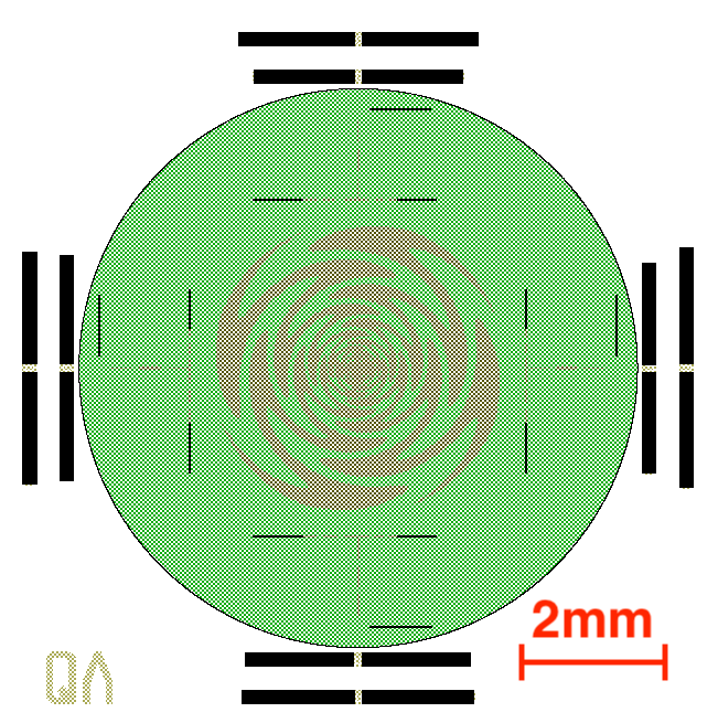
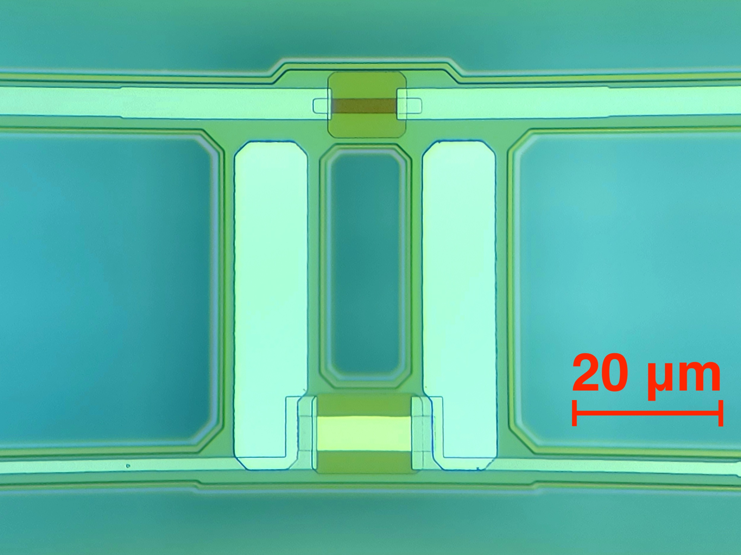
In a single pixel, once the radiation from the telescope excites the planar sinuous antenna, it couples to low-loss superconducting micro-strip transmission lines, which carry the photon through multiple lumped element pass-band and low-pass filters, multiple cross-unders for orthogonal polarizations and bands, and Radio-Frequency (RF) termination at the bolometer islands. These elements are shown in Figure 7(b).
2.2.1 Sinuous Antenna
Detailed descriptions, including important systematics of sinuous antennas, can be found in previous reports [1, 16]. We chose this technology for the LFT and MFT as its broadband nature is well suited to cover the frequency ranges required by LiteBIRD. For this application we describe the specific antenna used to fabricate a LF-4 prototype as shown in Figure 2.
2.2.2 TES Bolometers
The designs for the TES bolometers are quite similar for each band due the fact that they share a common operating temperature and CRE system. Small variations in expected optical loading will lead to different thermal conductance in each of the bolometers as the FPUs all operate at the same Bath Temperature (). The Superconducting Transition Temperature () the bolometers will be 170-200 mK the Normal Resistance () will be 1 . Once the conductance is tuned, the heat capacity of each bolometer is adjusted so that it has the same Intrinsic Time Constant () of 33 ms. As shown in Table 2, the bolometers are intended to be operated at a loopgains 10 for an operation time constant of 1.5 to 3 ms. More common bolometric parameters are shown in Table 2 and details of each band and expected optical power are shown in Table 1.
2.2.3 RF Filters
The details of the RF components vary from pixel to pixel and band to band, but the paradigm is the same for all of the pixels as all of the arrays define the pass-bands directly on the wafer using a combination of low-loss superconducting micro-strip transmission lines, on wafer pass-band definition, cross-unders for orthogonal polarizations, and RF termination at the bolometer island. For LiteBIRD the micro-strip lines are constructed with Niobium and a low-loss SiNx layer. Traditional RF circuit elements are patterned to the transmission lines to create the designed passbands. Table 1 summarizes the band centers and fractional bandwidths () for all of the LiteBIRD bands, which is typically 23% to 30%.
|
|
|
|
|
|
|
|
||||||||||||||||
| 40 | 0.3 | 70.5 | 0.2918 | ||||||||||||||||||||
| 60 | 0.23 | 51.1 | 0.2419 | ||||||||||||||||||||
| LF-1 | 32 | 24 | 78 | 0.23 | 43.8 | 0.2686 | |||||||||||||||||
| 50 | 0.3 | 58.5 | 0.306 | ||||||||||||||||||||
| 68 | 0.23 | 47.1 | 0.2709 | ||||||||||||||||||||
| LF12 | LF-2 | 32 | 12 | 89 | 0.23 | 41.5 | 0.2419 | ||||||||||||||||
| 68 | 0.23 | 41.6 | 0.3279 | ||||||||||||||||||||
| 89 | 0.23 | 33.0 | 0.3163 | ||||||||||||||||||||
| LF-3 | 16 | 72 | 119 | 0.3 | 26.3 | 0.3765 | |||||||||||||||||
| 78 | 0.23 | 36.9 | 0.3272 | ||||||||||||||||||||
| 100 | 0.23 | 30.2 | 0.3071 | ||||||||||||||||||||
| LF34 | LF-4 | 16 | 72 | 140 | 0.23 | 23.7 | 0.3557 |
| Design | Goal |
| Pixel in-band optical efficiency | 80% |
| Saturation Power () | 2-3X optical power |
| On-sky end-to-end yield | 80% |
| FPU | 100-120 mK |
| variation | 7% |
| TES | 1.0 |
| Operating TES resistance | 0.6 to 0.8 |
| Parasitic series resistance | 0.05 to 0.2 |
| 33 ms | |
| Loopgain during operation | 10 |
| Common 1/f-knee | 20 mHz |
| FPU lifetime | 3 years |
2.2.4 Cosmic Ray Mitigation
Following the lessons learned from the Planck satellite mission regarding the importance of mitigating cosmic ray events, our group has spent a considerable effort to building in mitigation techniques directly into both our detector and module designs [17]. At the detector level we have built prototypes with mitigation directly at the thermal isolation site of the bolometer as shown in Section 4.
For LiteBIRD bolometers will be thermally isolated and the wafers will be thermally sunk with a normal metal, such as Pd. Initial tests at UC Berkeley have shown these hardware implementations to work well [16].
2.3 Interface to Cryogenic Readout
The same niobium layer that forms the micro-strip layer is also used to route the TES bias/readout leads to the edges of the wafer to interface with the readout. For the Low-Frequency (LF) FPMs wiring density is low compared to ground-based arrays allowing for all of the TESs to be readout on a just two sides allowing for more flexibility with the design of the CRE interface. For the Mid-Frequency (MF) and High-Frequency (HF) FPMs, the wires are routed to all of the edges of the wafer for bonding.
We are minimizing the contribution of the CRE to the noise of the detection chain. The design principles are similar to that of SA and South Pole Telescope Third Generation (SPT-3G) where flexible circuitry makes electrical connections from the device wafer to lithographed inductor-capacitor (“LC”) chips. In previous experiments, a stripline which is up to a full meter in length sends the signals to Superconducting Quantum Interference Device (SQUID) arrays at 4 K. LiteBIRD has explored many options for how to use SQUID amplifiers at various cold stages to meet the noise requirements of LiteBIRD. To reduce the overall readout noise, the SQUIDs is integrated directly into the FPMs. This allows operation of the SQUIDs at colder temperatures and the ability to use shorter flexible circuitry for the initial step in the detection chain. A full detailed discussion of the development of the CRE for LiteBIRD can be found in Russell 2022[10].
3 Fabrication of LF-4 Prototypes
It will be the responsibility of UC Berkeley to fabricate the eight LF wafers as well as all of lenslet arrays for the LF-FPU and the MF-FPU. In this section, we report on the fabrication status for the MARS for the lenslets and the detector arrays for the 70/100/140 (LF-4) band.
3.1 MARS Fabrication
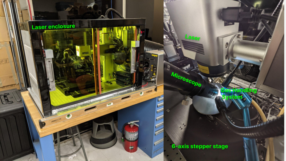
The MARS for the lenslets will be fabricated at UC Berkeley using a custom lasing-system. This system is comprised of a laser enclosure, the laser itself, which includes a galvanometer for precise laser scanning, a gas-handling system for process control, in-situ real time video microscopy, and a computer controlled 6-axis stepper motor system for precision placement of the lased holes as shown in Figure 4. This system is capable of producing sub-wavelength structures relevant to all of the lenslet-coupled bands in LiteBIRD[15].
3.1.1 Laser Enclosure
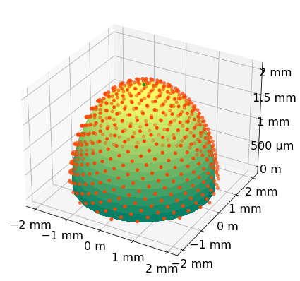
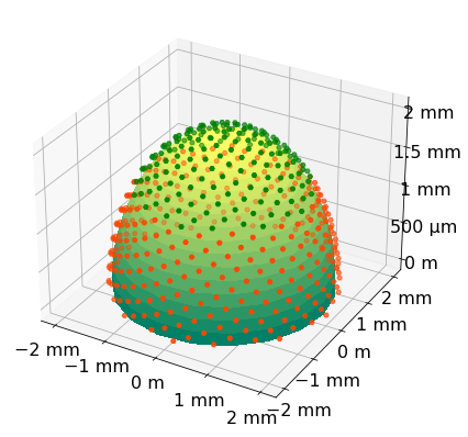
The laser enclosure consists of all of the necessary Class-1 safety precautions to provide researchers with proper safety during the laser-dicing process. The laser operates at 1064 nm and is capable of pulse-widths down to 2 ns, repetition rates up to 4 MHz, and powers up to 100 W with a minimum spot size of 34 m. Critically, this spot size is smaller than the largest feature size required for LiteBIRD MARS. Traditionally, laser machining of silicon requires femtosecond to picosecond pulse widths to avoid melted silicon and oxide production. The required structure is achieved with a relatively long, nanosecond pulse width by combining fast scanning of the laser galvanometer over the silicon surface with a gas handling system to actively clear silicon and reduce oxide production. This greatly improved the fidelity of pattern transfer of the desired to achieved shapes of the lased holes as shown in Figure 5. The gas handling system holds two high pressure nozzles at fixed locations that continuously flow high pressure nitrogen at the lasing site, as well as a third nozzle placed to remove residue across the surface of the sample. We also installed an in-situ microscope and video camera system to have real-time monitoring of the laser ablation which has provided valuable feedback to the manufacturing process. The final component of the laser system is the 6-axis stepper motor system with a step size of 0.625 m. This system will translate and rotate individual hemispheres underneath the lasing site to create the uniform arrays of holes on the surface. Software can generate arbitrary patterns on 3D surfaces to create any type of geometry. Figure 6 shows hypothetical locations to be lased by the laser on the surface of a hemisphere of silicon. Each red dot specifies a location on the lenslet surface that will be lased by manipulating the lenslet in 3D space underneath the laser.
3.1.2 Future Development of MARS
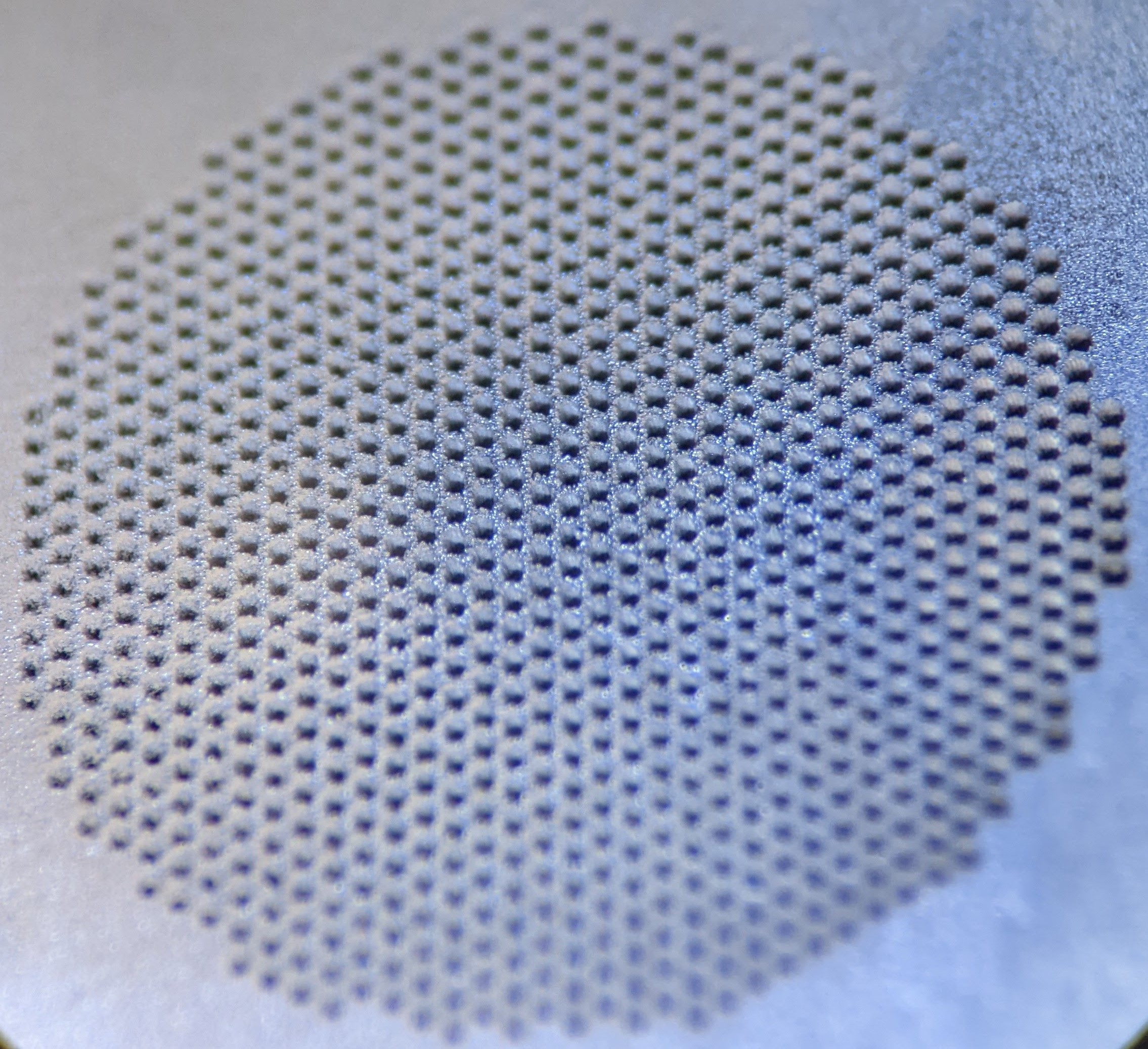
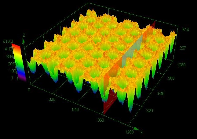
As a first step in the development in this technology, we have lased a single layer coating optimized for 150 GHz into a flat silicon substrate shown in Figure 5. In this demonstration, we laser-diced a MARS series of hexagonal holes in a closed-hex pattern on a silicon substrate. Each hole is a regular hexagon with a side length of 90 m laser-drilled to a depth of 270 m. There is a 30 m gap between the edges of nearest neighbors. Photographs and confocal microscopy scans of this pattern can be seen in Figure 5.
Future work will include the optimization for the seven different pixel types that will deploy lenslets with laser-ablated MARS. The 150 GHz MARS is very similar to the most challenging case of the MF-2 band, which requires good transmission up to 184 GHz.
3.2 Device Wafer Fabrication
The standard fabrication flow of sinuous antenna bolometers at MNL UC Berkeley is well described in previous technology development papers for LiteBIRD[11, 16]. These proceedings describes the initial ‘pre-processing’ fabrication steps we took to coat the back side of the wafers with palladium for cosmic ray mitigation.
3.2.1 Backside Palladium Deposition
As discussed in Section 2, mitigating cosmic ray events in the bolometer timestreams is critical to producing a high quality datasets for LiteBIRD. Simulations in COMSOL suggest that the presence of a normal metal such Pd or Au on the backside of the wafer will drastically reduce any signals in the TES as a result of a cosmic ray striking the substrate [18]. This presents a technical tension between coating the backside of the wafer with a normal metal while keeping the wafer optically transparent where the light from the telescope must pass through the wafer to stimulate the sinuous antenna. As such we have developed a Backside Cosmic Ray Mitigation Layer (BCRML) to solve this issue.
Although most of the fabrication steps that define the LB detector wafer; namely the antennae, filters, and bolometers; are processed on the frontside of the silicon wafer, there is an important and novel pre-process that occurs before the wafer is inserted into the frontside process flow. This is the process that defines the BCRML. The purpose of this structure is to minimize the time to recover from thermal noise caused by ballistic phonons from the impact of cosmic rays into the bulk of the silicon substrate.
For the work presented in this proceedings, a 0.5 m Pd BCRML film was patterned via a lift-off process using e-beam evaporation. In order to prepare the wafer for this step, the low Stress nitride (LSN) on the backside is removed to allow the BCRML to be in direct contact with the bulk silicon. Photo-resist is spun onto the frontside LSN film to protect it during the removal of the backside LSN and subsequent liftoff process. A simple CF4/O2 fluorine plasma etches the backside LSN down to the silicon substrate.
Lithography is performed on the backside of the wafer to create a lift off pattern for the holes in the Pd behind each antennas. When a 0.5 m film of Pd evaporated for the BCRML the resulting film has a tensile stress of 150 MPa. Experiments with a 2 m film yielded a tensile stress of 350 MPa. Thicker films of Pd may present a future technical challenge due to stress build up in this film.
Once the Pd BCRML was patterned, a passivation layer is added to the backside of the wafer both to; (1) to prevent Pd backside contamination of the wafer chucks on the tools used for five of the subsequent metallic and ceramic chlorine and fluorine plasma etches; and (2) to protect the Pd from the final corrosive XeF2 etch used to release the bolometer detectors from the bulk silicon.
The film chosen for this passivation is chemically inert and materially durable aluminum oxide. The deposition technique used is Atomic Layer Deposition (ALD) to ensure conformal coating of the backside. A 10 nm coating, deposited at 300 C for 20 minutes, was used. In testing, this thickness allowed protection from the XeF2 etch while still being thin enough to wirebond through for thermal grounding – a critical packaging element to assembling the full detector array.
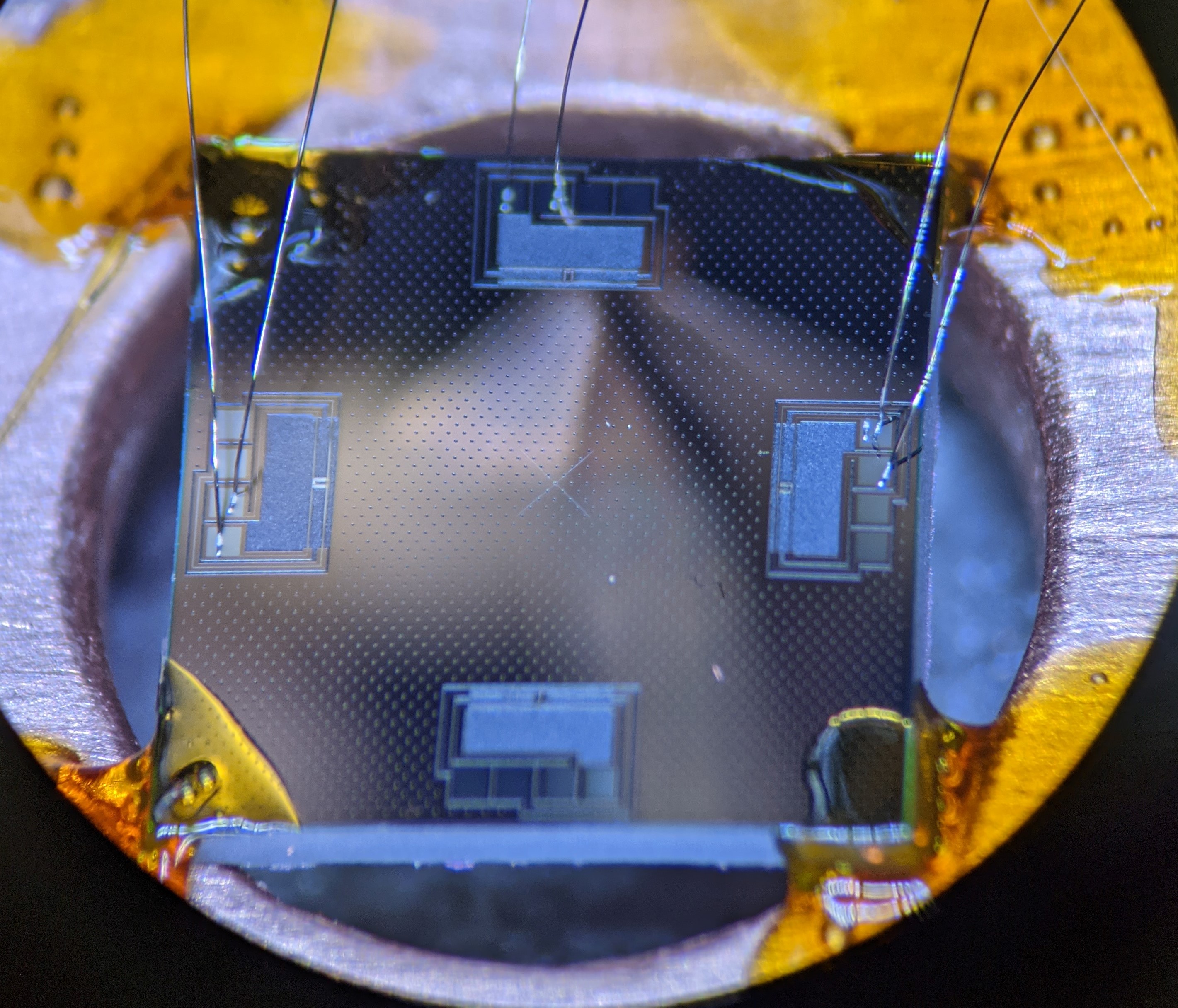
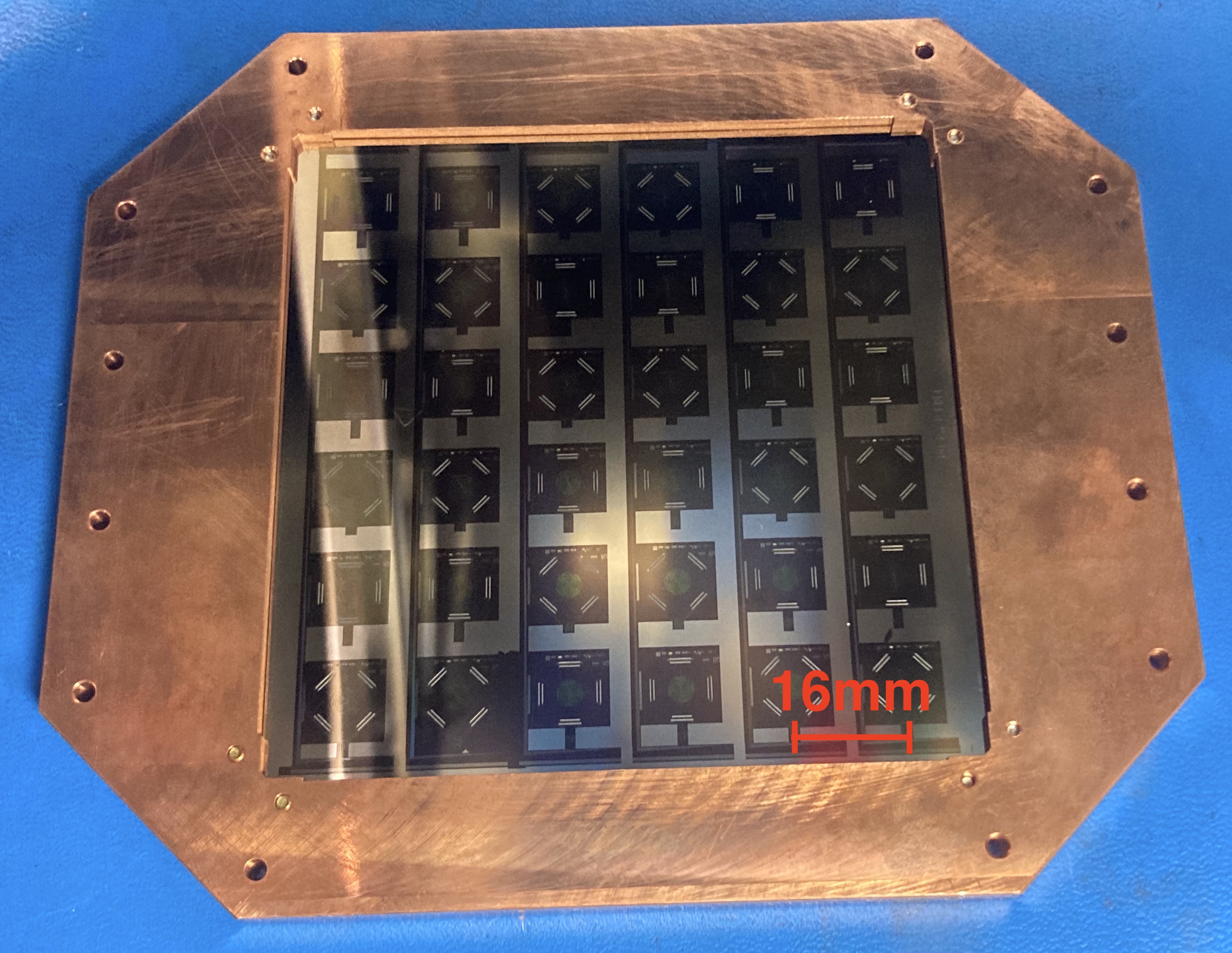
A prototype array with this extra Pd layer and micro-photographs of the devices on the front side is shown in Figure 7.
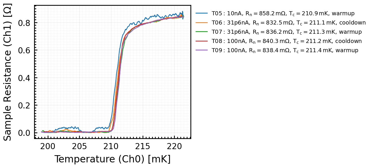
3.2.2 Tc Tuning
The LiteBIRD mission has a baseline plan to operate the FPUs at 100 mK with some contingency that allows for a higher base temperature. Based on our thermal modeling of the bolometers for LiteBIRD, we find that the optimal Tc for thermal carrier noise is 1.71 times the bath temperature which minimizes the thermal carrier noise of a TES bolometer dominated by phononic heat transport [13]. As such, a Tc range near 170 mK is targeted to meet the specifications of LiteBIRD.
To achieve this, the TESs is thermally annealed near the end of the fabrication process before the wafer is diced. While the exact mechanism is still to be determined, the of TESs increases monotonically when the substrate is baked at temperatures at or above 200 C. This means that any further thermal annealing can only increase the . As such, wafers can be thermally tuned for time and temperatures that produce a below the target and the thermal budget can be iteratively increased until the wafer has the desired . At this point, the wafer then is returned to the MNL where the final fabrication steps are carried out. This procedure ensures that we fabricate a wafer we are confident has TESs with the correct . Figure 10 in Section 4, shows resistance versus temperature measurements from LiteBIRD prototype LF-4 witness pixel.
4 Testing
UC Berkeley will characterize all of the Low-Frequency Focal Plane Modules (LF-FPMs) in the LF-FPU with support from University of Tokyo, CU, and Lawrence Berkeley National Laboratory (LBNL) [3, 10, 9]. The primary test cryostat is a BlueFors LD400 Dilution Refridgerator (DR) capable of cooling detector arrays to 100 mK. The system is currently capable of taking dark bolometric measurements to characterize TESs from full 6 inch wafer, diced device wafers, witness pixels, and test chips. The cyrostat houses 6 quantum design DC SQUIDs well suited to read out the properties of 1 LiteBIRD TESs.
4.1 Bolometric Testing
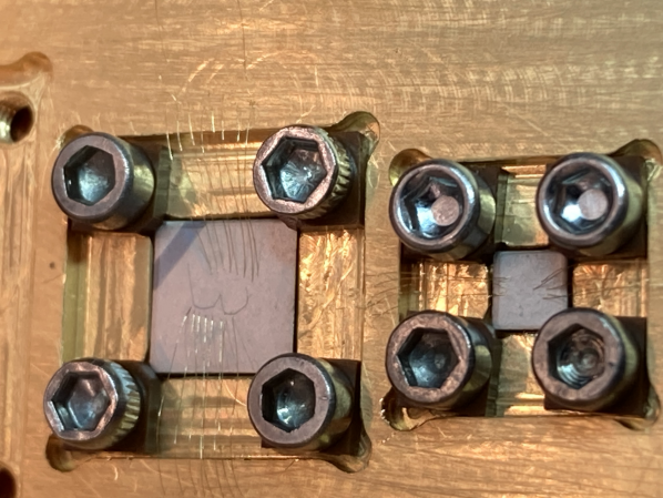
A novel feature of our fabrication and testing process is our ability to bond to an un-diced un-released device wafer. This improves our control on tuning the and of the devices. The scope of this testing is limited to measuring the stage temperature and sample resistance using four-wire resistance measurement with two LakeShore 372 AC resistance bridges. Photographs of this testing scheme are shown in Figure 9.
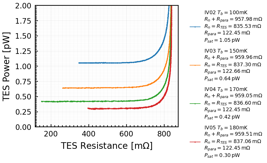
Prototype bolometers that are similar to what is expected to deploy for LiteBIRDhave been fabricated and tested. As shown in Table 1 the expected optical load on all of the bolometers is 0.25 to 0.4 pW, which with a safety factor of 2.5, requires bolometers to be fabricated with ranging from 0.6 to 1 pW. Characterization of a bolometer from a prototype of a LF-4 pixel has a saturation power just above this range as shown in Figure 10.
4.2 Cosmic Ray Testing
UC Berkeley is testing the efficacy of the cosmic ray mitigation techniques discussed in Section 2. To do this, we fabricate two chips that have bolometers with the same spacing and orientation and thermal properties. We apply mitigation to one of the chips and leave the other as a control as shown in chip Figure 9. Data is logged from the chips in various radiative environments to compare the total number of events and the number of coincidence in the two chips. A detailed discussion of the experimental setup for creating a hot cosmic ray environment can be found in a previous SPIE proceedings [16].
Simulation work from [18] suggest that a layer of normal metal deposited on the backside of the device wafer should be effective at reducing the amplitude and rate of cosmic ray signals seen in bolometers. The primary effect comes from the heat capacity and thermal conductivity of the Pd which helps keep the temperature of the substrate stable with minimal thermal gradients that could be caused by incident cosmic rays.
We plan to measure the efficacy of cosmic ray mitigation as a function of Pd thickness on the back side of the chip. Chips and wafers have been manufactured with 0, 0.5, and 2.0um of Pd and our currently running comparison tests at UC Berkeley on both full detector wafers and individual test chips while methods of depositing thicker layers of Pd on the back side of the wafer continue to be explored.
5 Summary
In these proceedings, we report on the design and fabrication status of the LF-FPMs for the LiteBIRD satellite mission. We describe the coupling architecture of the FPMs in detail and the methodology we used to achieve it. We are extending lenslet technology to be suitable for space flight by replacing traditional epoxy based Anti-Reflection Coatings (ARCs) with MARS laser-ablated into the surface of a silicon hemisphere. We have made significant progress on the the LF-4 pixel type including the fabrication of bolometers that meet the specifications of LiteBIRD.
6 Acknowledgments
The work in this proceeding is primarily funded by by NASA grant no. 80NSSC18K0132. This work is also supported in Japan by ISAS/JAXA for Pre-Phase A2 studies, by the acceleration program of JAXA research and development directorate, by the World Premier International Research Center Initiative (WPI) of MEXT, by the JSPS Core-to-Core Program of A. Advanced Research Networks, and by JSPS KAKENHI Grant Numbers JP15H05891, JP17H01115, and JP17H01125. The Italian LiteBIRD phase A contribution is supported by the Italian Space Agency (ASI Grants No. 2020-9-HH.0 and 2016-24-H.1-2018), the National Institute for Nuclear Physics (INFN) and the National Institute for Astrophysics (INAF). The French LiteBIRD phase A contribution is supported by the Centre National d’Etudes Spatiale (CNES), by the Centre National de la Recherche Scientifique (CNRS), and by the Commissariat à l’Energie Atomique (CEA). The Canadian contribution is supported by the Canadian Space Agency.
Norwegian participation in LiteBIRD is supported by the Research Council of Norway (Grant No. 263011). The Spanish LiteBIRD phase A contribution is supported by the Spanish Agencia Estatal de Investigación (AEI), project refs. PID2019-110610RB-C21 and AYA2017-84185-P. Funds that support contributions from Sweden come from the Swedish National Space Agency (SNSA/Rymdstyrelsen) and the Swedish Research Council (Reg. no. 2019-03959). The German participation in LiteBIRD is supported in part by the Excellence Cluster ORIGINS, which is funded by the Deutsche Forschungsgemeinschaft (DFG, German Research Foundation) under Germany’s Excellence Strategy (Grant No. EXC-2094 - 390783311). This research used resources of the Central Computing System owned and operated by the Computing Research Center at KEK, as well as resources of the National Energy Research Scientific Computing Center, a DOE Office of Science User Facility supported by the Office of Science of the U.S. Department of Energy.
LiteBIRD (phase A) activities are supported by the following funding sources: ISAS/JAXA, MEXT, JSPS, KEK (Japan); CSA (Canada); CNES, CNRS, CEA (France); DFG (Germany); ASI, INFN, INAF (Italy); RCN (Norway); AEI (Spain); SNSA, SRC (Sweden); NASA, DOE (USA).
References
- [1] LiteBIRD Collaboration, E. Allys, K. Arnold, J. Aumont, R. Aurlien, S. Azzoni, C. Baccigalupi, A. J. Banday, R. Banerji, R. B. Barreiro, N. Bartolo, L. Bautista, D. Beck, S. Beckman, M. Bersanelli, F. Boulanger, M. Brilenkov, M. Bucher, E. Calabrese, P. Campeti, A. Carones, F. J. Casas, A. Catalano, V. Chan, K. Cheung, Y. Chinone, S. E. Clark, F. Columbro, G. D’Alessandro, P. de Bernardis, T. de Haan, E. de la Hoz, M. De Petris, S. Della Torre, P. Diego-Palazuelos, T. Dotani, J. M. Duval, T. Elleflot, H. K. Eriksen, J. Errard, T. Essinger-Hileman, F. Finelli, R. Flauger, C. Franceschet, U. Fuskeland, M. Galloway, K. Ganga, M. Gerbino, M. Gervasi, R. T. Génova-Santos, T. Ghigna, S. Giardiello, E. Gjerløw, J. Grain, F. Grupp, A. Gruppuso, J. E. Gudmundsson, N. W. Halverson, P. Hargrave, T. Hasebe, M. Hasegawa, M. Hazumi, S. Henrot-Versillé, B. Hensley, L. T. Hergt, D. Herman, E. Hivon, R. A. Hlozek, A. L. Hornsby, Y. Hoshino, J. Hubmayr, K. Ichiki, T. Iida, H. Imada, H. Ishino, G. Jaehnig, N. Katayama, A. Kato, R. Keskitalo, T. Kisner, Y. Kobayashi, A. Kogut, K. Kohri, E. Komatsu, K. Komatsu, K. Konishi, N. Krachmalnicoff, C. L. Kuo, L. Lamagna, M. Lattanzi, A. T. Lee, C. Leloup, F. Levrier, E. Linder, G. Luzzi, J. Macias-Perez, B. Maffei, D. Maino, S. Mandelli, E. Martínez-González, S. Masi, M. Massa, S. Matarrese, F. T. Matsuda, T. Matsumura, L. Mele, M. Migliaccio, Y. Minami, A. Moggi, J. Montgomery, L. Montier, G. Morgante, B. Mot, Y. Nagano, T. Nagasaki, R. Nagata, R. Nakano, T. Namikawa, F. Nati, P. Natoli, S. Nerval, F. Noviello, K. Odagiri, S. Oguri, H. Ohsaki, L. Pagano, A. Paiella, D. Paoletti, A. Passerini, G. Patanchon, F. Piacentini, M. Piat, G. Polenta, D. Poletti, T. Prouvé, G. Puglisi, D. Rambaud, C. Raum, S. Realini, M. Reinecke, M. Remazeilles, A. Ritacco, G. Roudil, J. A. Rubino-Martin, M. Russell, H. Sakurai, Y. Sakurai, M. Sasaki, D. Scott, Y. Sekimoto, K. Shinozaki, M. Shiraishi, P. Shirron, G. Signorelli, F. Spinella, S. Stever, R. Stompor, S. Sugiyama, R. M. Sullivan, A. Suzuki, T. L. Svalheim, E. Switzer, R. Takaku, H. Takakura, Y. Takase, A. Tartari, Y. Terao, J. Thermeau, H. Thommesen, K. L. Thompson, M. Tomasi, M. Tominaga, M. Tristram, M. Tsuji, M. Tsujimoto, L. Vacher, P. Vielva, N. Vittorio, W. Wang, K. Watanuki, I. K. Wehus, J. Weller, B. Westbrook, J. Wilms, E. J. Wollack, J. Yumoto, and M. Zannoni, “Probing Cosmic Inflation with the LiteBIRD Cosmic Microwave Background Polarization Survey,” arXiv e-prints , p. arXiv:2202.02773, Feb. 2022.
- [2] M. Hazumi, P. A. R. Ade, A. Adler, E. Allys, K. Arnold, D. Auguste, J. Aumont, R. Aurlien, J. Austermann, C. Baccigalupi, A. J. Banday, R. Banjeri, R. B. Barreiro, S. Basak, J. Beall, D. Beck, S. Beckman, J. Bermejo, P. de Bernardis, M. Bersanelli, J. Bonis, J. Borrill, F. Boulanger, S. Bounissou, M. Brilenkov, M. Brown, M. Bucher, E. Calabrese, P. Campeti, A. Carones, F. J. Casas, A. Challinor, V. Chan, K. Cheung, Y. Chinone, J. F. Cliche, L. Colombo, F. Columbro, J. Cubas, A. Cukierman, D. Curtis, G. D’Alessandro, N. Dachlythra, M. De Petris, C. Dickinson, P. Diego-Palazuelos, M. Dobbs, T. Dotani, L. Duband, S. Duff, J. M. Duval, K. Ebisawa, T. Elleflot, H. K. Eriksen, J. Errard, T. Essinger-Hileman, F. Finelli, R. Flauger, C. Franceschet, U. Fuskeland, M. Galloway, K. Ganga, J. R. Gao, R. Genova-Santos, M. Gerbino, M. Gervasi, T. Ghigna, E. Gjerløw, M. L. Gradziel, J. Grain, F. Grupp, A. Gruppuso, J. E. Gudmundsson, T. de Haan, N. W. Halverson, P. Hargrave, T. Hasebe, M. Hasegawa, M. Hattori, S. Henrot-Versillé, D. Herman, D. Herranz, C. A. Hill, G. Hilton, Y. Hirota, E. Hivon, R. A. Hlozek, Y. Hoshino, E. de la Hoz, J. Hubmayr, K. Ichiki, T. Iida, H. Imada, K. Ishimura, H. Ishino, G. Jaehnig, T. Kaga, S. Kashima, N. Katayama, A. Kato, T. Kawasaki, R. Keskitalo, T. Kisner, Y. Kobayashi, N. Kogiso, A. Kogut, K. Kohri, E. Komatsu, K. Komatsu, K. Konishi, N. Krachmalnicoff, I. Kreykenbohm, C. L. Kuo, A. Kushino, L. Lamagna, J. V. Lanen, M. Lattanzi, A. T. Lee, C. Leloup, F. Levrier, E. Linder, T. Louis, G. Luzzi, T. Maciaszek, B. Maffei, D. Maino, M. Maki, S. Mandelli, E. Martinez-Gonzalez, S. Masi, T. Matsumura, A. Mennella, M. Migliaccio, Y. Minami, K. Mitsuda, J. Montgomery, L. Montier, G. Morgante, B. Mot, Y. Murata, J. A. Murphy, M. Nagai, Y. Nagano, T. Nagasaki, R. Nagata, S. Nakamura, T. Namikawa, P. Natoli, S. Nerval, T. Nishibori, H. Nishino, F. Noviello, C. O’Sullivan, H. Ogawa, H. Ogawa, S. Oguri, H. Ohsaki, I. S. Ohta, N. Okada, N. Okada, L. Pagano, A. Paiella, D. Paoletti, G. Patanchon, J. Peloton, F. Piacentini, G. Pisano, G. Polenta, D. Poletti, T. Prouvé, G. Puglisi, D. Rambaud, C. Raum, S. Realini, M. Reinecke, M. Remazeilles, A. Ritacco, G. Roudil, J. A. Rubino-Martin, M. Russell, H. Sakurai, Y. Sakurai, M. Sandri, M. Sasaki, G. Savini, D. Scott, J. Seibert, Y. Sekimoto, B. Sherwin, K. Shinozaki, M. Shiraishi, P. Shirron, G. Signorelli, G. Smecher, S. Stever, R. Stompor, H. Sugai, S. Sugiyama, A. Suzuki, J. Suzuki, T. L. Svalheim, E. Switzer, R. Takaku, H. Takakura, S. Takakura, Y. Takase, Y. Takeda, A. Tartari, E. Taylor, Y. Terao, H. Thommesen, K. L. Thompson, B. Thorne, T. Toda, M. Tomasi, M. Tominaga, N. Trappe, M. Tristram, M. Tsuji, M. Tsujimoto, C. Tucker, J. Ullom, G. Vermeulen, P. Vielva, F. Villa, M. Vissers, N. Vittorio, I. Wehus, J. Weller, B. Westbrook, J. Wilms, B. Winter, E. J. Wollack, N. Y. Yamasaki, T. Yoshida, J. Yumoto, M. Zannoni, and A. Zonca, “LiteBIRD satellite: JAXA’s new strategic L-class mission for all-sky surveys of cosmic microwave background polarization,” in Society of Photo-Optical Instrumentation Engineers (SPIE) Conference Series, Society of Photo-Optical Instrumentation Engineers (SPIE) Conference Series 11443, p. 114432F, Dec. 2020.
- [3] G. Jaehnig Submitted to SPIE 2022 , 2022.
- [4] L. E. Bleem et al., “Galaxy Clusters Discovered via the Sunyaev-Zel’dovich Effect in the 2500-square-degree SPT-SZ survey,” Astrophys. J. Suppl. 216(2), p. 27, 2015.
- [5] M. Abitbol et al., “The EBEX balloon-borne experiment—detectors and readout,” Astrophys. J. Suppl. 239, p. 8, Nov. 2018.
- [6] K. Arnold, P. A. Ade, A. Anthony, F. Aubin, D. Boettger, J. Borrill, C. Cantalupo, M. Dobbs, J. Errard, D. Flanigan, et al., “The polarbear cmb polarization experiment,” in Millimeter, Submillimeter, and Far-Infrared Detectors and Instrumentation for Astronomy V, 7741, p. 77411E, International Society for Optics and Photonics, 2010.
- [7] A. Suzuki, P. Ade, Y. Akiba, C. Aleman, K. Arnold, C. Baccigalupi, B. Barch, D. Barron, A. Bender, D. Boettger, J. Borrill, S. Chapman, Y. Chinone, A. Cukierman, M. Dobbs, A. Ducout, R. Dunner, T. Elleflot, J. Errard, G. Fabbian, S. Feeney, C. Feng, T. Fujino, G. Fuller, A. Gilbert, N. Goeckner-Wald, J. Groh, T. D. Haan, G. Hall, N. Halverson, T. Hamada, M. Hasegawa, K. Hattori, M. Hazumi, C. Hill, W. Holzapfel, Y. Hori, L. Howe, Y. Inoue, F. Irie, G. Jaehnig, A. Jaffe, O. Jeong, N. Katayama, J. Kaufman, K. Kazemzadeh, B. Keating, Z. Kermish, R. Keskitalo, T. Kisner, A. Kusaka, M. L. Jeune, A. Lee, D. Leon, E. Linder, L. Lowry, F. Matsuda, T. Matsumura, N. Miller, K. Mizukami, J. Montgomery, M. Navaroli, H. Nishino, J. Peloton, D. Poletti, G. Puglisi, G. Rebeiz, C. Raum, C. Reichardt, P. Richards, C. Ross, K. Rotermund, Y. Segawa, B. Sherwin, I. Shirley, P. Siritanasak, N. Stebor, R. Stompor, J. Suzuki, O. Tajima, S. Takada, S. Takakura, S. Takatori, A. Tikhomirov, T. Tomaru, B. Westbrook, N. Whitehorn, T. Yamashita, A. Zahn, and O. Zahn, “The Polarbear-2 and the Simons Array Experiments,” Journal of Low Temperature Physics 184, pp. 805–810, Aug. 2016.
- [8] M. H. Abitbol et al., “The Simons Observatory: Astro2020 Decadal Project Whitepaper,” Bull. Am. Astron. Soc. 51, p. 147, 2019.
- [9] T. Ghigna Submitted to SPIE 2022 , 2022.
- [10] M. Russell Submitted to SPIE 2022 , 2022.
- [11] B. Westbrook, P. A. R. Ade, M. Aguilar, Y. Aklba, K. Arnold, C. Baccigalupi, D. Barron, D. Beck, S. Beckman, and A. N. Bender, “The polarbear-2 and simons array focal plane fabrication status,” Journal of Low Temperature Physics (5).
- [12] F. W. Carter, T. W. Cecil, C. L. Chang, H.-M. Cho, J.-F. Cliche, T. M. Crawford, A. Cukierman, E. V. Denison, T. de Haan, J. Ding, M. A. Dobbs, D. Dutcher, W. Everett, A. Foster, J. C. Groh, A. Gilbert, N. W. Halverson, A. H. Harke-Hosemann, N. L. Harrington, J. W. Henning, G. C. Hilton, G. P. Holder, W. L. Holzapfel, N. Huang, K. D. Irwin, O. B. Jeong, M. Jonas, T. S. Khaire, L. Knox, A. M. Kofman, M. Korman, D. L. Kubik, S. Kuhlmann, C.-L. Kuo, A. T. Lee, E. M. Leitch, A. E. Lowitz, S. S. Meyer, D. Michalik, J. Montgomery, A. Nadolski, T. Natoli, H. Ngyuen, G. I. Noble, V. Novosad, S. Padin, Z. Pan, J. Pearson, C. M. Posada, A. Rahlin, C. L. Reichardt, J. E. Ruhl, J. T. Sayre, E. Shirokoff, G. Smecher, J. A. Sobrin, A. A. Stark, K. T. Story, A. Suzuki, K. L. Thompson, C. Tucker, L. R. Vale, K. Vanderlinde, J. Vieira, G. Wang, N. Whitehorn, V. Yefremenko, K. W. Yoon, M. Young, A. N. Bender, P. A. R. Ade, Z. Ahmed, A. J. Anderson, J. S. Avva, P. S. Barry, R. B. Thakur, B. A. Benson, L. S. Bleem, K. Byrum, J. E. Carlstrom, K. Aylor, S. Bocquet, S. Dodelson, J. Gallicchio, S. Guns, W. Quan, S. Raghunathan, W. L. Wu, and A. Jones, “Year two instrument status of the SPT-3g cosmic microwave background receiver,” in Millimeter, Submillimeter, and Far-Infrared Detectors and Instrumentation for Astronomy IX, J. Zmuidzinas and J.-R. Gao, eds., SPIE, Aug. 2018.
- [13] A. Suzuki, “Multichroic Bolometric Detector Architecture for Cosmic Microwave Background Polarimetry Experiments,” PhD thesis, University of California, Berkeley , 2013.
- [14] J. M. Edwards, R. O’Brient, A. T. Lee, and G. M. Rebeiz, “Dual-polarized sinuous antennas on extended hemispherical silicon lenses,” IEEE Transactions on Antennas and Propagation 60(9), pp. 4082–4091, 2012.
- [15] N. Farias, S. Beckman, A. T. Lee, and A. Suzuki, “Simulated performance of laser-machined metamaterial anti-reflection coatings,” Journal of Low Temperature Physics , 2022.
- [16] B. Westbrook, C. Raum, S. Beckman, A. T. Lee, N. Farias, T. Sasse, A. Suzuki, E. Kane, J. E. Austermann, J. A. Beall, S. M. Duff, J. Hubmayr, G. C. Hilton, J. V. Lanen, M. R. Vissers, M. R. Link, N. Halverson, G. Jaehnig, T. Ghinga, S. Stever, Y. Minami, K. L. Thompson, M. Russell, K. Arnold, J. Seibert, and M. Silva-Feaver, “Detector fabrication development for the LiteBIRD satellite mission,” in Space Telescopes and Instrumentation 2020: Optical, Infrared, and Millimeter Wave, M. Lystrup, M. D. Perrin, N. Batalha, N. Siegler, and E. C. Tong, eds., 11443, pp. 915 – 936, International Society for Optics and Photonics, SPIE, 2020.
- [17] A. Miniussi, J. L. Puget, W. Holmes, G. Patanchon, A. Catalano, Y. Giraud-Heraud, F. Pajot, M. Piat, and L. Vibert, “Study of Cosmic Ray Impact on Planck/HFI Low Temperature Detectors,” Journal of Low Temperature Physics 176, pp. 815–821, Sept. 2014.
- [18] S. L. Stever, T. Ghigna, M. Tominaga, G. Puglisi, M. Tsujimoto, M. Zeccoli Marazzini, M. Baratto, M. Tomasi, Y. Minami, S. Sugiyama, A. Kato, T. Matsumura, H. Ishino, G. Patanchon, and M. Hazumi, “Simulations of systematic effects arising from cosmic rays in the LiteBIRD space telescope, and effects on the measurements of CMB B-modes,” JCAP 2021, p. 013, Sept. 2021.