Single-crystalline PbTe film growth through reorientation
Abstract
Heteroepitaxy enables the engineering of novel properties, which do not exist in a single material. Two principle growth modes are identified for material combinations with large lattice mismatch, Volmer-Weber and Stranski-Krastanov. Both lead to the formation of three-dimensional islands, hampering the growth of flat defect-free thin films. This limits the number of viable material combinations. Here, we report a distinct growth mode found in molecular beam epitaxy of PbTe on InP initiated by pre-growth surface treatments. Early nucleation forms islands analogous to the Volmer-Weber growth mode, but film closure exhibits a flat surface with atomic terracing. Remarkably, despite multiple distinct crystal orientations found in the initial islands, the final film is single-crystalline. This is possible due to a reorientation process occurring during island coalescence, facilitating high quality heteroepitaxy despite the large lattice mismatch, difference in crystal structures and diverging thermal expansion coefficients of PbTe and InP. This growth mode offers a new strategy for the heteroepitaxy of dissimilar materials and expands the realm of possible material combinations.
I. Introduction
Heteroepitaxy has been a staple of modern material science enabling a wide variety of techniques such as band alignment tuning and surface passivation,Lauhon.2002 crystal structure transfer,Fadaly.2020 superlattices,Mundy.2016 strain engineering,Schaeffler.1997 and virtual substrates.Bioud.2019 Strictly two-dimensional layer-by-layer growth ensues if adatoms are more strongly bound to the substrate than to each other.Frank.1949 For the heteroepitaxy of dissimilar materials, this is generally not possible.Palmstrom.1995 Instead, if the adatoms are more strongly bound to each other than to the substrate, they follow the Volmer-Weber growth mode with the formation of three-dimensional islands.Volmer.1926 Alternatively, in the intermediate Stranski-Krastanov case, initial layer-by-layer growth occurs until a critical thickness is reached where island growth ensues.Stranski.1937 The two latter options lead to a three-dimensional surface topography with a high defect density.Floro.2001 ; Mo.1990 ; Teichert.2002 This can be detrimental to the desired material characteristics or geometry, limiting the viable material combinations.
A prime example for a research field dependent on artificially structured materials with stringent quality requirements is topological quantum computation. Here, inherently fault-tolerant qubits have been proposed, based on the non-abelian braiding statistics exhibited by Majorana bound states.Kitaev.2001 ; Kitaev.2003 ; Nayak.2008 ; Sarma.2015 Suitable solid-state systems rely heavily on deliberate material design, with proposals suggesting the use of semiconductor nanowire networks on an electrically isolating substrate, partially coupled to epitaxially grown superconducting islands.Lutchyn.2010 ; Oreg.2010 ; Karzig.2017 ; Plugge.2017 Despite significant advances in the fabrication of the heterostructures,Chang.2015 ; Guel.2017 ; Krizek.2018 ; Heedt.2021 ; Kanne.2021 a definite proof of the existence of Majorana bound states is lacking. A major challenge is posed by material limitations causing disorder, e.g. surface roughness, charge impurities, point defects, atomic vacancies, patterning imperfections, or geometric restrictions.Pan.2020 ; Sarma.2021 ; Woods.2021 ; Ahn.2021 The ability to reduce this disorder is critical for the development of Majorana qubits and solid state based quantum technologies more broadly, making high quality heteroepitaxy imperative.
In this work, we explore the molecular beam epitaxy of PbTe on InP (111)A substrates. The lead-salt is an attractive material choice for topological quantum computation,Springholz.1993 ; Grabecki.1999 ; Grabecki.2004 ; Chitta.2005 ; Chitta.2006 ; Grabecki.2006 ; Wuttig.2018 ; Geng.2021 ; Schellingerhout.2022 ; Cao.2022 ; Jiang.2022 ; Kate.2022 ; Jung.2022 suppressing disorder due to the screening of charged impurity scattering, resulting from the large dielectric constant.Yuan.1997 ; Grabecki.2005 InP is a suitable substrate due to the insulating properties, availability, and well developed processing schemes. The growth initially follows the Volmer-Weber model, forming islands that subsequently coalesce, percolate, and finally, in response to a pre-growth surface treatment, form a closed film exhibiting a terrace-stepped surface. An involved crystal reorientation process facilitates the growth of large single-crystalline PbTe films regardless of the significant lattice mismatch, different crystal structure, and diverging thermal expansion coefficient between growth and substrate. Reorientation processes have previously only been shown in metals compensating small angle mismatches between islands of about °.Pashley.1964 High quality growth on a comparable material combination has been reported, however no reorientation process was observed, as initial islands exhibited only one epitaxial orientation upon surface treatments.Haidet.2020 Understanding and exploiting the described growth mechanism can open paths to new high quality heterostructures involving dissimilar materials.
II. PbTe Layer Formation
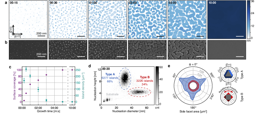
A time series, depicted in Fig. 1a-b, explores the growth behaviour of PbTe on (111)A InP substrates. Initially, discrete islands are formed, visible already at 15 s growth time. The islands subsequently expand both vertically and laterally, until they begin to coalesce. The film has almost fully percolated at 3 min, after which it forms a closed layer exhibiting atomic terracing which only forms in consequence of a pre-growth surface treatment (see Supplementary Information Fig. S1). This film formation behaviour is summarised in Fig. 1c, where island density and surface coverage are plotted over time. Initially, the observed increase of surface coverage is driven both by creation of new and expansion of existing islands. However, around 30 s, new nuclei stop forming and islands begin to coalesce, resulting in a decrease in the island density. The distributions of island height and diameter support the cessation of new island formation. This is shown for 30 s growth time as a two-dimensional histogram in Fig. 1d. The lack of a tail into the small island heights and diameters imply a homogeneity in the age of the nuclei, where the presence of a certain density of islands blocks the formation of new islands. This indicates a reasonable diffusion length of growth species over the InP substrate, as atoms impinging on the substrate are prevented from forming a new island by diffusing to an existing one. Consequently, these islands compete for material. Fig. 1d reveals not only a narrow spread for both displayed quantities, but also a bimodal distribution. This is a result of two distinct types of islands with different aspect ratios, hereafter referred to as type (66%) and type (34%). Analysis across different growth times confirms that islands of both types form before 15 s growth time and grow in both vertical and lateral directions with type dependent rates (see Supplementary Information Fig. S2). Using surface normals extracted from the atomic force microscopy (AFM) data, the polar plot in Fig. 1e reveals the distribution of side facet orientations of the 30 s grown islands, separated by type. The presence of maxima indicates a preferential epitaxial orientation of Type islands, with the corresponding facets indicated in the inset Wulff-construction. The absence of any preferred orientation in type islands suggests by contrast an in-plane rotational freedom.
III. Epitaxial Orientation of Islands
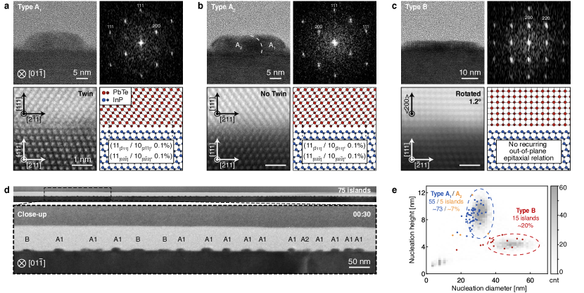
Transmission electron microscopy (TEM) analysis of the 30 s grown sample reveals three island types, each defined by a distinct epitaxial relation to the substrate. A representative high-resolution TEM image of the most frequent type, , is shown in Fig. 2a. This type is characterised by a twinned epitaxial relation between PbTe and InP, as confirmed by the micrograph’s fast Fourier transform (FFT). This results in a and interface along the in-plane directions transverse and parallel to the depicted zone axis. A high-angle annular dark-field (HAADF) scanning TEM image of an equivalent interface reveals the atomic planes of both crystal phases and establishes a structural model of the lattice. The large lattice mismatch of is overcome through the formation of edge-type misfit dislocations at the InP-PbTe interface, breaking bonds in exchange for a reduction of strain. For type , an lattice plane ratio is found in-plane, leading to 0.1% residual mismatch in the corresponding ideal flat interface. The less frequent type shown in Fig. 2b exhibits no interfacial twinning. The and crystal directions are a direct continuation of the substrate, with an identical lattice plain ratio and residual mismatch as type due to the structural similarity. In contrast to both types , type changes out-of-plane crystal direction at the interface from [111] to . Despite this distinct out-of-plane direction, no preferential in-plane orientation can be found, suggesting a weak adhesive force between the substrate and this island type.Miceli.1995 Due to this, no recurring lattice plain ratio or residual mismatch can be assigned to this island type. A bright-field TEM micrograph of the complete cross-section with 75 islands is shown in Fig. 2d. Several labelled islands can be seen in the close-up. In Fig. 2e the diameter and height values of islands found in the cross-section cut, measured via TEM, are compared to the AFM data presented in Fig. 1e. Tip convolution effects during the AFM measurement likely lead to an overestimation of the island diameter, in addition to the uncertainties introduced by the TEM projection. Despite these inherent inaccuracies, a close agreement between these measurement modalities is found, connecting the TEM based epitaxial relation of the island types with the superior statistics of the AFM data.
IV. Reorientation Upon Coalescence
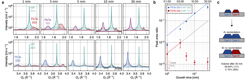
In light of the various crystal orientations present during the initial growth stages, it is of particular interest to study the mechanics leading to a closed film with atomically flat terraces. The stable lattice plane orientation throughout the growth (see Supplementary Information Fig. S3) enables their study through symmetric - XRD scans. Fig. 3a plots sections of the scattered X-ray intensity for increasing growth times. Fitting the XRD-spectra with pseudo-Voigt functions allows for the identification of the isolated InP (111), PbTe (111), and PbTe (200) peaks and their higher order reflections. The two PbTe peaks correspond to type and epitaxy, respectively. No indications of other orientations can be found, confirming the absence of additional types (see Supplementary Information Fig. S4). The area under each peak is correlated with the probed volume of that crystal orientation.Als.2020 Fig. 3b compares the peak area of PbTe (222) and PbTe (200) with growth time as an indication of the crystal growth evolution. Each calculated area is normalised with the InP peak area to eliminate any influence originating from varying sample size and alignment. The first noticeable characteristic of the plot is the steady increase of the PbTe (222) volume. As expected, the same behaviour is found for PbTe (111) (see Supplementary Information Fig. S4). In contrast to this, following an initial increase, the probed (200) crystal volume decreases by nearly an order of magnitude. No new orientations appear in the XRD spectra, pointing towards a reorientation process of the initial type nuclei into type . Based on the growth time dependency, the reorientation likely takes place upon island coalescence up until the subsequent film percolation. A sketch of the proposed process is shown in Fig. 3c. However, not all islands undergo this reorientation process as evident from the remaining PbTe (200) signal at 30 min growth time. This is supported by the continuously decreasing (200) peak width in Fig. 3a, a sign of ongoing vertical growth of those grains. Together with the initial (200) area decrease, this excludes overgrowth of the nuclei as a possible explanation of the observed phenomena, and instead suggests the coexistence of a small volume fraction of remaining (200) type grains at the PbTe growth front (see Supplementary Information Fig. S4). We note that this can likely be further optimised. Reciprocal space maps of asymmetric reflections distinguish twinned and non-twinned (111) PbTe layers, and are used to quantify the ratio between type and type in the layer (see Supplementary Information Fig. S5). Already at 3 min growth time all (111) oriented PbTe is found to be twinned relative to the InP substrate, i.e. only type remains. This is consistent with respective TEM observations.Jung.2022 Island orientation and morphology are governed by the interfacial and surface free energies. Additionally, there can be a bulk contribution in the form of strain energy, and contributions stemming from defects or grain boundaries. For reorientation to occur, it must both lead to a lower energy state and not have too high of an energy barrier. The relative influence of the substrate on the islands is expected to decline over time as the surface to volume ratio decreases. As such, it is unlikely that the reorientation of islands occurs spontaneously as the islands grow. The introduction of grain boundaries between different island types is therefore identified as the most probable trigger for reorientation. As the reorientation process occurs predominately to exclusively from type and towards type , the substrate interface plays a directing role in the reorientation, suggesting a minimal interfacial energy for type islands. It is difficult to overemphasise the importance of the reorientation process, as it facilitates the heteroepitaxy of high-quality thin films on dissimilar substrates, in this case PbTe (111) on InP (111)A. In fact, the seemingly unfit substrate with its large lattice mismatch, different crystal structure, and diverging thermal expansion coefficient, are believed to lead to a weak adhesive force between substrate and growth, facilitating the reorientation process.
V. Layer Mosaicity
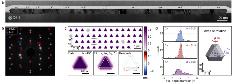
The crystal quality resulting from the reorientation process is assessed via TEM. A cross-section of a selective area grown (SAG) m structure shows subtle contrast variations throughout the film. These become pronounced when imaged off zone axis, as depicted in Fig. 4a. Despite these boundaries and despite the film originating from many islands with various epitaxial orientations, the complete cross-section has a single twinned epitaxial relation to the substrate, confirming the observations made in Fig. 3. This finding is supported by equivalent electron diffraction patterns taken across the complete segment (see Supplementary Information Fig. S6). A representative example is shown in Fig. 4b. The contrast variations visible in Fig. 4a are identified as boundaries between slightly misoriented segments, where the misorientation is a rotation around the surface normal of the substrate. The rotations are distributed between 0° and 0.5° and have a positive mean, indicating that in addition to individual variation, there is a common rotation relative to the substrate. The average relative rotation between neighbouring segments is 0.2°. This corresponds to a shift of one lattice plane about every 287 columns (about 185 nm in the PbTe crystal), and therefore amounts to, at most, a few planes offset over the length of each segment. This confirms that the PbTe films are single-crystalline, accompanied by slight mosaicity. The segment boundaries are not a result of incomplete reorientation between coalescing pairs of islands of different types. Based on the AFM data presented in Fig. 1, on average 7 islands, of which 2 type , combine to form a single segment of type . This suggests that multiple islands combine and reorient to form a strain free segment. To inspect the origin of the strain features, nanostructures were selectively grown from circular openings with a 200 nm diameter as shown in Fig. 4c. Based on the segment dimensions visible in TEM, the structures are expected to consist on average of a single segment. As such, measurements of their orientations can be compared to segment orientations in films before their merging. The facets formed in the nanostructures belong to the and families and can be reproduced via Wulff construction.Jung.2022 Based on the crystal symmetry, a fitting function is defined and used to acquire both facet radii and misorientation in three axes of rotation. A representative fit is shown in the bottom panel of Fig. 4c. A histogram over 155 fitted structures is depicted for each rotational axis in Fig. 4d. The found standard deviation of the out of plane rotation is 0.36°. This includes noise from imperfect facets, AFM measurement, and fitting and therefore gives an upper bound to the variation in structure orientations. The distribution suggests, that the origin of the strain features can be found in slight misalignments between meeting grains, that have become too large in size to align completely.
VI. Conclusion
To summarise, we present a distinct growth mode facilitating high quality heteroepitaxy of dissimilar materials by example of PbTe on InP (111)A substrates. AFM measurements reveal the three-dimensional islands present in early stages of the growth, and the eventual formation of a closed film. Structural differences in the initial islands are attributed to three distinct epitaxial orientations. XRD scans following the subsequent growth stages expose a reorientation process, facilitating the formation of a predominantly single-crystalline film. A fascinating outcome, considering the initial differences in epitaxial orientation of the nuclei. Small-angle misalignment is detected between segments of the film leading to strain signatures exposed by off zone axis TEM. Nevertheless, our recent quantum experiments on selective area grown structures employing the same growth mechanism yield electron mobilities comparable to InSb and a coherence length exceeding any previously reported values on selective area grown networks, signifying the high crystal quality of the PbTe.Jung.2022 Future work will explore the heteroepitaxial growth of topological crystalline insulators, namely SnTe and PbSnTe, that are expected to exhibit comparable growth behaviour.
Methods
Substrate fabrication
Undoped semi-insulating (111)A InP substrates were used as growth substrates. Selective area growth required additional processing as described in an accompanying publication.Jung.2022
PbTe heteroepitaxy
Growth took place in an ultra-high vacuum molecular beam epitaxy system. An annealing step under Te overpressure at 480 °C was used for surface reconstruction of the etched openings and to remove oxide residuals from the exposed substrate surface. The PbTe films were subsequently grown at 340 °C with separate elemental sources, providing a Te flux of about mbar and a Pb flux of about mbar measured as beam equivalent pressure using a naked bayard-alpert ion gauge. Temperatures were measured with a kSA BandiT system based on the optical absorption edge.
TEM studies
TEM lamellas were prepared in a FEI Nova Nanolab 600i as described in a previous publication.Jung.2021 TEM studies were performed using a probe-corrected JEOL ARM 20OF, equipped with a 100 mm2 Centurio SDD Energy dispersive X-ray spectroscopy detector.
Reported grain misorientations in Fig. 4a are based on tilt differences between the zone axis of the substrate and each individual grain in scanning TEM.
Modelling
All structural simulations of the NW crystals in Figs 2 were done using the Vesta software.Momma.2011
X-ray crystallography
XRD studies were carried out using a PanAlytical X’Pert Pro MRD diffractometer, equipped with a Cu K- radiation source. The scans were taken with a 1D detector, with pixels distributed along the 2 direction. The detector width was set to 1.2° degrees to suppress the background for the 1 min growth sample. Other measurements used the full detector width of 2.5°.
Large-scale statistics about the evolution of PbTe (200) and PbTe (111) were obtained using a beam spot of approximately mm. Fitting the spectra was done by fixing the background level on the average number of counts between 1/Å.
The normalisation with the InP substrate peak implicitly assumes that the PbTe film is transparent for X-rays. This is not completely correct, as the heavy elements Pb and Te are efficient at scattering X-rays. As a result, normalisation with the InP peak overestimates the PbTe/InP ratio. This overestimation becomes worse with increasing film thickness, and is therefore not an explanation for the observed (200) decrease after 3 mins of growth.
AFM studies and data processing Atomic force microscopy was performed using a Bruker Dimension Icon and a Bruker SCANASYST-AIR probe with a 2 nm tip radius and 0.4 N/m spring constant (nominal) via the SCANASYST acquisition mode. The scan size was with a resolution of 2048 by 2048 pixels and a scan rate of 0.5 Hz.
Detilting: The scans were detilted in two steps. First, by subtracting a plane with with an orientation matching the median gradient found in the scan and second by fitting and subtracting a line to each line in the scan direction.
Substrate level calibration: Zero height was determined for the scans with surface coverages below 100% by fitting a bimodal Gaussian distribution to a histogram of the entire detilted scan. The lower Gaussian’s center height was then defined to be the substrate surface level. For scans with surface coverages of 100%, a separate scan was carried out on the boundary between the mask and the opening, extracting the height above the mask of the structure and adding that to the thickness of the mask measured on a different sample from the same wafer.
Fitting: Fitting in panel 4c is carried out through least-squares minimisation. The in-plane structure’s centre is also fitted, this removes the necessity of independently fitting the radii of the three facets. A correlation matrix for all fitting parameters is shown in Supplementary Information Fig. S7.
References
- (1) Lauhon, L. J., Gudiksen, M. S., Wang, D. & Lieber, C. M. Epitaxial core–shell and core–multishell nanowire heterostructures. Nature 420, 57–61 (2002).
- (2) Fadaly, E. M. T. et al. Direct-bandgap emission from hexagonal Ge and SiGe alloys. Nature 580, 205–209 (2020). eprint 1911.00726.
- (3) Mundy, J. A. et al. Atomically engineered ferroic layers yield a room-temperature magnetoelectric multiferroic. Nature 537, 523–527 (2016).
- (4) Schäffler, F. High-mobility Si and Ge structures. Semiconductor Science and Technology 12, 1515 (1997).
- (5) Bioud, Y. A. et al. Uprooting defects to enable high-performance III–V optoelectronic devices on silicon. Nature Communications 10, 4322 (2019).
- (6) Frank, F. C. & Merwe, J. H. v. d. One-dimensional dislocations. I. Static theory. Proceedings of the Royal Society of London. Series A. Mathematical and Physical Sciences 198, 205–216 (1949).
- (7) Palmstrom, C. J. Epitaxy of dissimilar materials. Annual Review of Materials Science 25, 389–415 (1995).
- (8) Volmer, M. & Weber, A. Keimbildung in übersättigten Gebilden. Zeitschrift für Physikalische Chemie 119U, 277–301 (1926).
- (9) Stranski, I. N. & Krastanow, L. Zur Theorie der orientierten Ausscheidung von Ionenkristallen aufeinander. Monatshefte für Chemie und verwandte Teile anderer Wissenschaften 71, 351–364 (1937).
- (10) Floro, J. A. et al. The dynamic competition between stress generation and relaxation mechanisms during coalescence of Volmer–Weber thin films. Journal of Applied Physics 89, 4886–4897 (2001).
- (11) Mo, Y.-W., Savage, D. E., Swartzentruber, B. S. & Lagally, M. G. Kinetic pathway in Stranski-Krastanov growth of Ge on Si(001). Physical Review Letters 65, 1020–1023 (1990).
- (12) Teichert, C. Self-organization of nanostructures in semiconductor heteroepitaxy. Physics Reports 365, 335–432 (2002).
- (13) Kitaev, A. Y. Unpaired Majorana fermions in quantum wires. Physics-Uspekhi 44, 131 (2001). eprint cond-mat/0010440.
- (14) Kitaev, A. Fault-tolerant quantum computation by anyons. Annals of Physics 303, 2–30 (2003). eprint quant-ph/9707021.
- (15) Nayak, C., Simon, S. H., Stern, A., Freedman, M. & Sarma, S. D. Non-Abelian anyons and topological quantum computation. Reviews of Modern Physics 80, 1083–1159 (2008). eprint 0707.1889.
- (16) Sarma, S. D., Freedman, M. & Nayak, C. Majorana zero modes and topological quantum computation. npj Quantum Information 1, 15001 (2015). eprint 1501.02813.
- (17) Lutchyn, R. M., Sau, J. D. & Sarma, S. D. Majorana fermions and a topological phase transition in semiconductor-superconductor heterostructures. Physical Review Letters 105, 077001 (2010). eprint 1002.4033.
- (18) Oreg, Y., Refael, G. & Oppen, F. v. Helical liquids and majorana bound states in quantum wires. Physical Review Letters 105, 177002 (2010). eprint 1003.1145.
- (19) Karzig, T. et al. Scalable designs for quasiparticle-poisoning-protected topological quantum computation with Majorana zero modes. Physical Review B 95, 235305 (2017). eprint 1610.05289.
- (20) Plugge, S., Rasmussen, A., Egger, R. & Flensberg, K. Majorana box qubits. New Journal of Physics 19, 012001 (2017). eprint 1609.01697.
- (21) Chang, W. et al. Hard gap in epitaxial semiconductor–superconductor nanowires. Nature Nanotechnology 10, 232–236 (2015). eprint 1411.6255.
- (22) Gül, Ö. et al. Hard superconducting gap in insb nanowires. Nano Letters 17, 2690–2696 (2017). eprint 1702.02578.
- (23) Krizek, F. et al. Field effect enhancement in buffered quantum nanowire networks. Physical Review Materials 2, 093401 (2018). eprint 1802.07808.
- (24) Heedt, S. et al. Shadow-wall lithography of ballistic superconductor–semiconductor quantum devices. Nature Communications 12, 4914 (2021). eprint 2007.14383.
- (25) Kanne, T. et al. Epitaxial Pb on InAs nanowires for quantum devices. Nature Nanotechnology 16, 776–781 (2021). eprint 2002.11641.
- (26) Pan, H. & Sarma, S. D. Physical mechanisms for zero-bias conductance peaks in Majorana nanowires. Physical Review Research 2, 013377 (2020). eprint 1910.11413.
- (27) Sarma, S. D. & Pan, H. Disorder-induced zero-bias peaks in Majorana nanowires. Physical Review B 103, 195158 (2021). eprint 2103.05628.
- (28) Woods, B. D., Sarma, S. D. & Stanescu, T. D. Charge-impurity effects in hybrid majorana nanowires. Physical Review Applied 16, 054053 (2021). eprint 2103.06880.
- (29) Ahn, S., Pan, H., Woods, B., Stanescu, T. D. & Sarma, S. D. Estimating disorder and its adverse effects in semiconductor Majorana nanowires. arXiv (2021). eprint 2109.00007.
- (30) Springholz, G., Bauer, G. & Ihninger, G. MBE of high mobility PbTe films and PbTe/Pb1-xEuxTe heterostructures. Journal of Crystal Growth 127, 302–307 (1993).
- (31) Grabecki, G. et al. Quantum ballistic transport in constrictions of n-PbTe. Physical Review B 60, R5133–R5136 (1999). eprint cond-mat/9906178.
- (32) Grabecki, G. et al. Ballistic transport in PbTe-based nanostructures. Physica E: Low-dimensional Systems and Nanostructures 20, 236–245 (2004).
- (33) Chitta, V. A. et al. Multivalley transport and the integer quantum Hall effect in a PbTe quantum well. Physical Review B 72, 195326 (2005).
- (34) Chitta, V. et al. Integer quantum Hall effect in a PbTe quantum well. Physica E: Low-dimensional Systems and Nanostructures 34, 124–127 (2006).
- (35) Grabecki, G. et al. PbTe—A new medium for quantum ballistic devices. Physica E: Low-dimensional Systems and Nanostructures 34, 560–563 (2006).
- (36) Wuttig, M., Deringer, V. L., Gonze, X., Bichara, C. & Raty, J.-Y. Incipient metals: Functional materials with a unique bonding mechanism. Advanced Materials 30, 1803777 (2018).
- (37) Geng, Z. et al. Observation of Aharonov-Bohm effect in PbTe nanowire networks. arXiv (2021). eprint 2112.11900.
- (38) Schellingerhout, S. G. et al. Growth of PbTe nanowires by molecular beam epitaxy. Materials for Quantum Technology 2, 015001 (2022).
- (39) Cao, Z. et al. Numerical study of PbTe-Pb hybrid nanowires for engineering Majorana zero modes. Physical Review B 105, 085424 (2022). eprint 2110.13803.
- (40) Jiang, Y. et al. Selective area epitaxy of PbTe-Pb hybrid nanowires on a lattice-matched substrate. Physical Review Materials 6, 034205 (2022). PbTe in-plane growth MBE CdTe, eprint 2110.13642.
- (41) Kate, S. C. t. et al. Large even-odd spacing and g-factor anisotropy in PbTe quantum dots. arxiv (May, 2022).
- (42) Jung, J. et al. Selective area growth of PbTe nanowire networks on InP. arXiv (2022).
- (43) Yuan, S. et al. Magnetoreflectivity of Pb1-xEuxTe epilayers and PbTe/Pb1-xEuxTe multiple quantum wells. Physical Review B 55, 4607–4619 (1997).
- (44) Grabecki, G. et al. Disorder suppression and precise conductance quantization in constrictions of PbTe quantum wells. Physical Review B 72, 125332 (2005). eprint cond-mat/0506756.
- (45) Pashley, D. W., Stowell, M. J., Jacobs, M. H. & Law, T. J. The growth and structure of gold and silver deposits formed by evaporation inside an electron microscope. Philosophical Magazine 10, 127–158 (1964).
- (46) Haidet, B. B., Hughes, E. T. & Mukherjee, K. Nucleation control and interface structure of rocksalt PbSe on (001) zincblende III-V surfaces. Physical Review Materials 4, 033402 (2020).
- (47) Miceli, P. F. & Palmstro/m, C. J. X-ray scattering from rotational disorder in epitaxial films: An unconventional mosaic crystal. Physical Review B 51, 5506–5509 (1995).
- (48) Als‐Nielsen, J. & McMorrow, D. Elements of Modern X‐ray Physics, Chapter 5: “Kinematical scattering II: crystalline order (John Wiley & Sons, 2020).
- (49) Jung, J. et al. Universal platform for scalable semiconductor‐superconductor nanowire networks. Advanced Functional Materials 31 (2021).
- (50) Momma, K. & Izumi, F. VESTA3 for three-dimensional visualization of crystal, volumetric and morphology data. Journal of Applied Crystallography 44, 1272–1276 (2011).
Acknowledgements
We thank NanoLab@TU/e for their help and support.
This work has been supported by the European Research Council (ERC TOCINA 834290) and TOPSQUAD (Grant No. 862046).
We furthermore acknowledge Solliance, a solar energy R&D initiative of ECN, TNO, Holst, TU/e, IMEC and Forschungszentrum Jülich, and the Dutch province of Noord-Brabant for funding the TEM facility.
Author Contributions
J.J. and S.G.S. carried out the substrate fabrication and the growth of PbTe.
O.A.H.v.d.M. and J.J. performed the AFM characterisation and data analysis.
W.H.J.P. performed and analysed the XRD measurements.
M.A.V. performed the TEM analysis.
J.J. and S.G.S. prepared FIB lamellae.
M.A.V. and E.P.A.M.B. provided key suggestions and discussions and supervised the project.
J.J. and O.A.H.v.d.M. wrote the manuscript, with contributions from all authors.
Competing Interests
The authors declare no competing interests.
Additional Information
Supplementary Information is available for this paper.
Correspondence should be addressed to to E.P.A.M.B. (e.p.a.m.bakkers@tue.nl).
Data Availability The data supporting the findings of this study is openly available at https://doi.org/10.5281/zenodo.6900774