Tunneling processes between Yu-Shiba-Rusinov bound states
Abstract
Very recent experiments have reported the tunneling between Yu-Shiba-Rusinov (YSR) bound states at the atomic scale. These experiments have been realized with the help of a scanning tunneling microscope where a superconducting tip is functionalized with a magnetic impurity and is used to probe another magnetic impurity deposited on a superconducting substrate. In this way it has become possible to study for the first time the spin-dependent transport between individual superconducting bound states. Motivated by these experiments, we present here a comprehensive theoretical study of the tunneling processes between YSR bound states in a system in which two magnetic impurities are coupled to superconducting leads. Our theory is based on a combination of an Anderson model with broken spin degeneracy to describe the impurities and nonequilibrium Green’s function techniques to compute the current-voltage characteristics. This combination allows us to describe the spin-dependent transport for an arbitrary strength of the tunnel coupling between the impurities. We first focus on the tunnel regime and show that our theory naturally explains the experimental observations of the appearance of current peaks in the subgap region due to both the direct and thermal tunneling between the YSR states in both impurities. Then, we study in detail the case of junctions with increasing transparency, which has not been experimentally explored yet, and predict the occurrence of a large variety of (multiple) Andreev reflections mediated by YSR states that give rise to a very rich structure in the subgap current. In particular, we predict the occurrence of multiple Andreev reflections that involve YSR states in different impurities. These processes have no analogue in single-impurity junctions and they are manifested as current peaks with negative differential conductance for subgap voltages. Overall, our work illustrates the unique physics that emerges when the spin degree of freedom is added to a system with superconducting bound states.
I Introduction
In recent years, the competition between magnetism and superconductivity has been extensively studied at the atomic scale with the help of the scanning tunneling microscope (STM). With this instrument it is possible to manipulate individual magnetic atoms and molecules and study the electronic transport through them when they are deposited on a superconducting substrate. In these single-impurity systems, the combination of spin-dependent scattering and superconductivity leads to the appearance of the so-called Yu-Shiba-Rusinov (YSR) states Yu1965 ; Shiba1968 ; Rusinov1969 , which are superconducting bound states with unique properties such as their spin polarization. Many STM-based experiments have demonstrated the existence of these bound states and, in turn, have elucidated many of their basic properties Yazdani1997 ; Ji2008 ; Franke2011 ; Menard2015 ; Ruby2015 ; Hatter2015 ; Ruby2016 ; Randeria2016 ; Choi2017 ; Cornils2017 ; Hatter2017 ; Farinacci2018 ; Brand2018 ; Malavolti2018 ; Kezilebieke2019 ; Senkpiel2019 ; Schneider2019 ; Liebhaber2020 ; Huang2020b ; Odobesko2020 , for a recent review see Ref. Heinrich2018 . Part of the interest in the physics of YSR states lies in the fact that they can be viewed as building blocks to create Majorana states in designer structures such as chains of magnetic impurities Nadj-Perge2014 ; Ruby2015b ; Kezilebieke2018 ; Ruby2017 ; Ruby2018 .
Very recently, it has been experimentally demonstrated that a superconducting STM tip can be decorated with a magnetic impurity that then features YSR states Huang2020a . More importantly, this YSR-STM can, in turn, be used to probe other magnetic impurities deposited on a superconducting substrate and that also features YSR states. In this way, the experiments realized for the first the time the tunneling between individual superconducting bound states at the atomic scale, which is the ultimate limit for quantum transport. Additionally, it has been shown that the YSR-STM can be used to measure the intrinsic lifetime of YSR states and that the tunnel current exhibits peaks in the subgap region due to direct and thermal tunneling between the YSR in both impurities Huang2020a . In particular, those current peaks can be used to extract information about the relative orientation between the impurity spins Huang2020c . In fact, this system represents an ideal platform to explore the interplay between spin-dependent transport and superconductivity, which lies at the heart of the field of superconducting spintronics Linder2015 ; Eschrig2015 ; Holmqvist2018 . On the other hand, it is obvious that the YSR-STM may have important implications for spin-polarized scanning tunneling microscopy and the study of atomic-scale magnetic structures, as it has been nicely demonstrated in Ref. Schneider2020 .
Another exciting possibility that the YSR-STM opens up is the study of the interplay between superconducting bound states and (multiple) Andreev reflections in a situation never explored before and in which the spin degree of freedom plays a central role. Let us recall that in a junction with at least one superconducting electrode, an Andreev reflection consists of a tunneling process in which an electron coming from a normal metal is reflected as a hole of opposite spin transferring a Cooper pair into the superconductor. In the absence of in-gap bound states, this process dominates the subgap transport. If the junction features two superconducting leads, one can additionally have multiple Andreev reflections (MARs) in which quasiparticles undergo a cascade of Andreev reflections that give rise to a very rich subgap structure in the current-voltage characteristics. The microscopic theory of MARs for spin-degenerate quantum point contacts was developed in the mid-1990s Averin1995 ; Cuevas1996 , and it was first quantitatively confirmed in the context of superconducting atomic-size contacts with the help of break-junction techniques and the STM Scheer1997 ; Scheer1998 . In recent years, different STM experiments in the context of magnetic impurities on superconducting surfaces and using superconducting tips have revealed signatures of the interplay between YSR bound states and Andreev reflections Ruby2015 ; Randeria2016 ; Farinacci2018 ; Brand2018 ; Huang2020c . From the theory side, we have recently put forward a model to describe this interplay in single-impurity junctions and have shown how the spin degree of freedom leads to MAR processes that have no analogue in nonmagnetic systems. The qualitative predictions of this theory have been experimentally confirmed Huang2020c . The goal of this work is to extend that theoretical analysis to the two-impurity case in order to elucidate the different tunneling processes that can take place between YSR states.
In this work we present a systematic study of the tunneling processes between YSR bound states in a system comprising two magnetic impurities that are coupled to their respective superconducting electrodes, see Fig. 1. Our theory is based on the use of a mean-field Anderson model with broken spin symmetry to describe the magnetic impurities and we employ the Keldysh formalism to compute the current-voltage characteristics for arbitrary junction transmission, i.e., to any order in the tunnel coupling between the two impurities. To illustrate the power of our model, we first focus on the analysis of the tunnel regime in which the charge transport is completely dominated by tunneling of single quasiparticles. In this regime, we naturally explain the basic observations reported in Refs. Huang2020a ; Huang2020c concerning the presence of current peaks with huge negative differential conductance in the gap region. As explained in Refs. Huang2020a ; Huang2020c , those peaks can be attributed to the direct and thermal tunneling between the YSR states in both impurities and their heights contain sufficient information to extract the relative orientation of the impurity spins. More importantly, we also study in detail how the transport characteristics change upon increasing the junction transparency and predict the occurrence of several families of MARs that give rise to an extremely rich subgap structure in the current and differential conductance. In particular, we find a series of MARs that start and end in YSR bound states, which are not possible in the case of single-impurity junctions. The signature of these YSR-mediated MARs is a series of current peaks at certain subgap voltages determined by the energy of the YSR states in both impurities. All the predictions put forward in this work can, in principle, be verified with the exact system investigated in Refs. Huang2020a ; Huang2020c .
The rest of the manuscript is organized as follows. In Sec. II we describe the system under study and present the model and theoretical tools that we have employed to study the electronic transport in our two-impurity superconducting system. In Sec. III we focus on the tunnel regime and show how our theory nicely explains all the basic observations reported in Refs. Huang2020a ; Huang2020c . Then, in Sec. IV we present a detailed study of the subgap transport in junctions with a moderate-to-high transmission and analyze the interplay between MARs and YSR states. Finally, in Sec. V we summarize our main conclusions.
II System under study and theoretical approach
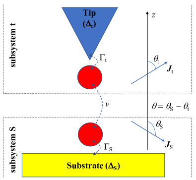
The goal of this work is to elucidate the different tunneling processes that can occur between YSR states. As explained in the introduction, these bound states appear in single magnetic impurities (atoms or molecules) coupled to superconducting electrodes and the tunneling between them is possible via direct inter-impurity coupling. This system has been realized with the help of an STM and, in this case, an impurity is coupled to the superconducting STM tip, while the other one is coupled to a superconducting substrate Huang2020a , as we show schematically in Fig. 1. Thus, our technical goal is to compute the current-voltage characteristics in such a system and this section is devoted to a detailed description of the model and theoretical tools employed for this purpose.
We consider the total system shown in Fig. 1 and assume that the magnetic moments of the impurities form a relative angle , which will be treated as a parameter of the model. Motivated by the experiments of Ref. Huang2020a , we shall assume that the impurities are strongly coupled to their respective electrode (STM tip and substrate), which is the regime in which the YSR states appear. In this sense, in order to describe the electronic transport in this system, it is natural to divide it into two subsystems, tip (t) and substrate (S), each one containing a magnetic impurity which is strongly coupled to a superconducting electrode. Moreover, we shall assume that the voltage drops at the interface between the two impurities. Such a system can be modeled by a generic point-contact Hamiltonian of the form
| (1) |
where with describes the corresponding subsystem (i.e., an impurity coupled its superconducting electrode) and describes the tunnel coupling between these two subsystems. These different parts of the total Hamiltonian will be specified in the following subsections.
II.1 Bare Green’s function of a magnetic impurity coupled to a superconductor and YSR states
The impurities are described with a mean-field Anderson model with broken spin symmetry that was recently used to describe the role of the impurity-substrate coupling Huang2020b and to elucidate the MARs that can take place in the electronic transport through a single magnetic impurity coupled to superconducting leads Villas2020 . This model has also been successfully employed in the past to describe the observation of Andreev bound states in quantum dots coupled to superconducting leads and it has been shown to reproduce many of the salient features of the superconducting bound states predicted by more sophisticated many-body approaches Martin-Rodero2011 ; Martin-Rodero2012 . Within this model, we couple the magnetic impurity featuring a single energy level and a magnetization , where is the angle between the magnetization and a global quantization axis along the direction, to an s-wave superconductor. It is convenient to first focus on the individual subsystems described by and define the Hamiltonians and the effective Green’s functions in each individual diagonal basis pointing along the direction of . The two separate bases are then simply related to the global quantization axis by a rotation of the above defined angle about the axis in spin space.
First, we define the spinors along the global quantization axis as
| (2a) | ||||
| (2b) | ||||
which consist of annihilation (creation) operators and for electrons on the dot and the superconductor, respectively, with spin and quasi-momentum . The Hamiltonian of the subsystem reads
| (3) |
where describes the magnetic impurity in subsystem , describes the superconducting electrode in subsystem , and describes their coupling in subsystem . As it has been shown in Ref. Villas2020 , by using the spinors in Eq. (2) these Hamiltonians can be cast into the form
| (4a) | ||||
| (4b) | ||||
| (4c) | ||||
with the matrix Hamiltonians
| (5a) | ||||
| (5b) | ||||
| (5c) | ||||
Here, is the electronic energy in the superconductor, and are the pairing potential and the superconducting phase, respectively, and is the tunnel coupling between the impurity and the superconductor. Furthermore, and are Pauli matrices in spin and Nambu space, respectively, while and are the corresponding unit matrices in these spaces.
To simplify the formalism, it is convenient to transfer the dependence on and to the coupling term in Eq. (1) and work with Hamiltonians describing the subsystems in which the corresponding spin points along its quantization axis. Therefore, we introduce the combined unitary transformation in the Hamiltonian defined in Eq. (4) to rotate the individual bases defined in Eq. (2) to the quantization axis in subsystem along and to remove the phase . This results in the new bases and and the transformed Hamiltonians
| (6a) | ||||
| (6b) | ||||
The starting point for the calculation of the electronic transport in the system under study is the calculation of the bare Green’s function of the impurity coupled to the superconductor in each subsystem . Following the exact same steps of the calculation presented in Ref. Villas2020 , we derive the block-diagonal bare matrix Green’s function in the new basis , i.e.,
| (7) |
where the two blocks are given by
| (8) |
with the denominator
| (9) |
Along the derivation, we defined , and the tunneling rates , where is the normal density of states at the Fermi energy in superconductor .
The current-voltage characteristics of this system will reflect the electronic structure of the magnetic impurities and, in particular, the presence of YSR states Villas2020 ; Huang2020b . From Eqs. (7) and (8), it follows that the electronic local density of states (LDOS) projected onto the impurity site is given by
| (10) |
with
| (11) |
where retarded (r) and advanced (a) Green’s functions are defined as by introducing the phenomenological Dynes parameter which describes the inelastic broadening of the electronic states in electrode . The condition for the appearance of superconducting bound states is . In particular, the spin-induced YSR states appear in the limit and they are inside the gap when also . In this case, there is a pair of fully spin-polarized YSR bound states at energies (measured with respect to the Fermi energy) Villas2020 ; Huang2020b
| (12) |
which in the electron-hole symmetric case reduces to
| (13) |
II.2 Tunnel coupling between two impurities
The tunnel coupling in Eq. (1) between the two subsystems with the global quantization axis defined by Eq. (2a) reads
| (14) |
with and the tunnel coupling between the two impurities Villas2020 . Introducing the aforementioned basis rotation in subsystem results in
| (15) |
where
| (16a) | ||||
| (16b) | ||||
is the relative angle, and the superconducting phase difference between the two impurities. In that sense, the coupling between the two subsystems is effectively represented by a spin-active interface in which there are spin-flip processes whose probabilities depend on the relative orientation of the impurity spins described by .
II.3 Calculation of the current-voltage characteristics
To compute the electronic transport properties in our model system, we shall assume that the voltage drops at the interface between the two impurities, which is justified by the fact that usually the impurity-impurity coupling is much weaker than the impurity-electrode couplings . Under this assumption, our system effectively reduces to a superconducting quantum point contact and we can compute its transport properties with a generalization of the MAR theory of Ref. Cuevas1996 to account for the spin-dependent transport. This generalization was in fact developed in our previous work of Ref. Villas2020 and we simply reproduce the formalism here to make this manuscript more self-contained and to emphasize the peculiarities introduced by the spin-flip processes between the two impurities.
Our goal is to compute the current in our two-impurity system under an external bias voltage . As in any superconducting contact, the bias voltage induces a time-dependent superconducting phase difference that varies linearly in time with the bias. This can be simply included in the formalism by replacing with in Eq. (16) such that acquires a time dependence . The theory of Ref. Cuevas1996 is based on nonequilibrium Green’s function techniques (or Keldysh formalism) and a central role is played by the lesser matrix Green’s functions
| (17) |
for and where and are the rotated four-component spinors defined above. In addition, is the time-ordering operator on the Keldysh contour such that any time in the lower branch () is larger than any time in the upper one (). The electrical current in our system is defined as , where is the number operator in subsystem S, and it can be expressed in terms of as Villas2020
| (18) |
where Tr is the trace taken over spin and Nambu degrees of freedom.
The task is now to compute the dressed Green’s functions appearing in the current formula. For this purpose, we follow a perturbative scheme and treat the coupling term in the Hamiltonian of Eq. (1) as a perturbation. The unperturbed Green’s functions correspond to the uncoupled impurity-electrode subsystems in equilibrium and are given by Eq. (7). On the other hand, to solve the problem it is convenient to express the current in terms of the so-called -matrix. The -matrix associated with the time-dependent perturbation is defined as
| (19) |
where the product is a shorthand for convolution, i.e., for integration over intermediate time arguments. As shown in Ref. Cuevas1996 , the exact current to all orders in the tunneling rate can be written in terms of the -matrix components as
| (20) |
It is convenient to Fourier transform with respect to the temporal arguments to solve the -matrix integral equations:
| (21) |
Because of the time dependence of the coupling matrices, one can show that admits the following general solution
| (22) |
Thus, it follows that the current exhibits a time dependence in the form of the Fourier series
| (23) |
where the current amplitudes can be expressed in terms of the components and as
| (24) |
Notice that the bare Green’s functions are diagonal in energy space and the bare lesser Green’s functions are given by , where is the Fermi function with temperature and the Boltzmann constant . The previous formula can be further simplified by using the general relation , which reduces the calculation of the current to the determination of the Fourier components fulfilling the set of linear algebraic equations
| (25) |
where the different matrix coefficients are given in terms of the unperturbed Green’s functions as
| (26a) | ||||
| (26b) | ||||
| (26c) | ||||
| (26d) | ||||
| (26e) | ||||
In general, these block-tridiagonal systems have to be solved numerically and the current can only be expressed in an analytical form in the tunnel regime, as we discuss in Sec. III. On the other hand, let us stress that we shall focus here exclusively on the discussion of the dc current, i.e., in Eq. (23), and we shall not analyze the (zero-bias) dc Josephson current (or supercurrent).
II.4 Normal state conductance
To get insight into the current in our system, it is didactic to consider the case in which the electrodes are in the normal state. Moreover, the analysis of this case gives us the chance to introduce the normal state conductance, , which is the physical parameter that allows to make contact with the experiment. In the case in which neither the tip nor the substrate are superconducting, the current formula within our model can be worked out analytically and it is given by the following Landauer-type of expression
| (27) |
where are the transmission coefficients for electron tunneling processes connecting spins and . In general, the expressions of these coefficients in terms of the different parameters of the model are extremely cumbersome and in what follows, we only provide such expressions in certain limiting cases. First of all, in the tunnel regime, where , we find
| (28a) | ||||
| (28b) | ||||
where . Notice that, as expected, the coefficient for antiparallel spins vanishes when . Moreover, in the limit in which we are interested, namely the limit when YSR states appear, one can safely ignore the energy and bias dependence of these transmission coefficients. On the other hand, and to give an idea about these coefficients beyond the tunnel regime, we consider the case of parallel spin (). In this case (ignoring the bias dependence),
| (29a) | ||||
| (29b) | ||||
In general, the zero-temperature normal state linear conductance in our system is given by
| (30) |
where is the quantum of conductance. Moreover, in this work, will always be much smaller than such that the differential conductance in the normal state will be independent of the bias.
III Tunnel regime
So far, the experiments on the tunneling between YSR states have been performed in the so-called tunnel regime, in which the coupling between the impurities is relatively weak and the only transport process that takes place is single-quasiparticle tunneling (eventually involving the YSR states) Huang2020a . This regime has already been addressed in Refs. Huang2020a ; Huang2020c and we want to expand that discussion in this section in the light of the model described in the previous section.
Let us recall that the main experimental observation reported in Ref. Huang2020a is the appearance of current peaks inside the gap region that can be associated with the quasiparticle tunneling between the YSR states of the two impurities. Let us now show how this observation can be naturally explained within our model. In our case, the tunnel regime can be roughly defined as the limit in which the tunnel coupling is sufficiently weak such that and the only relevant tunneling process is the single-quasiparticle tunneling. In this limit, we can use the approximation in Eq. (25) and after some straightforward algebra we arrive at the following expression for the tunneling current at the lowest order in the tunnel coupling between the impurities
| (31) | |||||
Let us recall that in this expression is the hopping element that describes the coupling between the impurities, is the Fermi function, is the angle defining the relative orientation of the impurity spins, and is the LDOS on the impurity site for spin ( stands for the spin antiparallel to ), which is given by Eq. (11). The current formula of Eq. (31) has the expected structure for a tunnel junction with a spin-active interface. As usual in those junctions, we have two types of processes: (i) tunnel events involving parallel spins (terms weighted by ) and (ii) tunnel events involving antiparallel spins (terms weighted by ). When both electrodes are in the normal states, this result reduces to that described in Sec. II.4 for the tunnel regime.
In Fig. 2 we illustrate the results obtained with the tunnel formula above for three different values of the angle together with a schematic description of the processes. In this example, as in all cases discussed in this manuscript, we assume equal superconducting gaps for the tip and the substrate and set (to be in the strong coupling regime realized in STM experiments in which YSR states appear). Additionally, we have and for the impurity coupled to the substrate, and and for the impurity coupled to the tip (the large values of , comparable to , are necessary for the YSR states to be well inside the gap). With these parameter values, the YSR states in both impurities appear at energies and (we assume that ). Finally, we have assumed a finite temperature of .
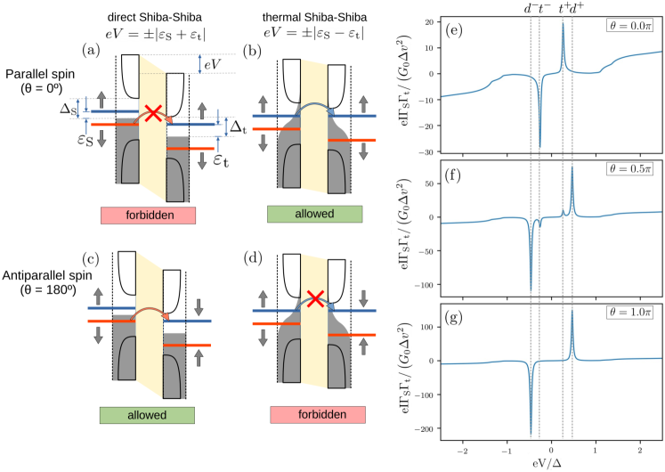
The result for parallel spins () is shown in panel Fig. 2(e). In this case, the most salient feature is the appearance of two current peaks inside the gap region at a bias . Since in this case the impurity spins are parallel, the tunneling between the lower YSR state in one impurity and the upper state in the other impurity is forbidden, as we illustrate in Fig. 2(a). Notice that in this example both impurities have the same type of ground state, i.e., they are on the same side of the quantum critical point (the point in parameter space for which the YSR states appear at zero energy and the spin of the ground state changes). Thus, a subgap current peak in the tunnel regime for can only be due to the tunneling between the two upper (or two lower) states, which is possible due to the finite temperature and the corresponding partial occupation of the different states, see Fig. 2(b). For this reason, we refer to these peaks as thermal Shiba-Shiba peaks and denote their height as and for positive () and negative () bias. Notice that in this case because of the lack of electron-hole symmetry in the tip impurity ().
Let us now discuss the case of antiparallel spins () shown in Fig. 2(g). In this case, the tunneling between the lower and upper YSR states is allowed, see Fig. 2(c), and this process gives rise to current bias at , which explains the subgap structure shown in Fig. 2(g). We refer to the peaks originating from this tunneling process as direct Shiba-Shiba peaks and we denote their height as and for positive () and negative () bias. Again, the fact that in this example is due to the electron-hole asymmetry in the tip impurity. In the case of antiparallel spins (), the thermally activated processes described in the previous paragraph are forbidden, see Fig. 2(d), which explains the absence of the corresponding peaks at , see Fig. 2(g).
For an intermediate situation, when the impurity spins are neither parallel nor antiparallel, both types of processes, direct and thermal Shiba-Shiba tunneling, are possible and both types of current peaks appear simultaneously at a finite temperature. This is illustrated in Fig. 2(f) where we show the result for .
Let us recall that in the experiments of Refs. Huang2020a ; Huang2020c , both types of peaks were observed at sufficiently high temperatures, which was interpreted as a sign that the spins were neither parallel nor antiparallel. Actually, the detailed analysis presented in Ref. Huang2020c suggested that there was no magnetic anisotropy fixing the relative spin orientation and that the spins in that experiment were freely rotating. In that case, the current measured in practice is an average over all possible values of the angle , which can be trivially done from Eq. (31) using , where denotes the angular average. The averaged current turns out to be equal to the current given by Eq. (31) for . Thus, the example of Fig. 2(f) describes precisely this averaged current in a situation where varies rapidly in time.
An important finding of Ref. Huang2020c was that the relative orientation between the impurity spins, i.e., the angle , can be extracted from the ratio between the thermal and the direct Shiba-Shiba peak. This conclusion was drawn with the help of the classical Shiba model Shiba1968 and our goal now is to show that it can also be derived from the Anderson model used in this work. To obtain the height of the different current peaks we first need analytical expressions for the LDOS describing the YSR states. From Eq. (11), it is easy to show that the spin-dependent impurity LDOS for energies close to the bound states adopt a Lorentzian-like form given by
| (32) |
where is a positive constant and describes the broadening (or inverse lifetime) of the corresponding bound state in impurity . The constants depend on the different parameters of the model, but the corresponding expressions are not important for our discussion here. Substituting Eq. (32) into the current formula of Eq. (31), we can compute the height of the different peaks. Of importance here is the ratio involving the height of the four different peaks, thermal and direct for positive and negative bias. It is straightforward to show that in the limit in which , which is almost always the case even for very low temperatures, this ratio is given by
| (33) |
which is the result derived in Ref. Huang2020c . Moreover, if , which is often the case, the previous formula reduces to
| (34) |
As explained in Ref. Huang2020c , the importance of this result is that the relative orientation between the impurity spins can be obtained from quantities (the current peak heights and the temperature) that can be directly measured. Here, we show that this result is quite universal and it does not depend on the details of the impurity model, as long as electron correlations can be ignored.
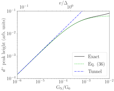
Another interesting observation reported in Ref. Huang2020a is the fact that the height of the peaks (and their area) undergoes a crossover between a linear regime at very low transmission (or normal state conductance) and a sublinear regime at higher transmission when the STM tip with its impurity was brought closer to the impurity on the substrate. Obviously, the tunnel approximation of Eq. (31) can only explain the linear regime in which the current, including the current peak heights, is proportional to and, in turn, to the normal state conductance. This perturbative result must fail at some point upon increasing the tunnel coupling, or reducing the bound state broadening, because times the product of density of states is no longer a small parameter. This has nothing to do with the occurrence of MARs, which were negligible in the experiments of Ref. Huang2020a . Thus, in order to describe the crossover to a sublinear regime, we must take into account the multiple normal reflections that may take place in the resonant electron tunneling between two sharp bound states (as in any resonant tunneling situation). In our case, this can be achieved by neglecting the anomalous Green’s function in the -matrix equations, which amounts to ignore the Andreev reflections, and solving them to infinite order in the tunnel coupling. Technically speaking, this is done by approximating Eq. (25) by
| (35) |
where, in addition, the anomalous Green’s functions (off-diagonal components in Nambu space) are set to zero in the expression of . Then, the solution of this equation can be introduced in the current formula of Eq. (II.3). Finally, after some algebra and retaining only the lowest order terms in in the numerator, we arrive at the following improved formula for the tunneling current
| (36) | |||||
with
| (37) | |||||
where the expressions of the different bare Green’s functions appearing here can be found in Eq. (8). Notice that this modified tunneling formula is very similar to the original one, see Eq. (31), the only difference being the presence of the denominator . This denominator takes into account the possible normal reflections in the tunneling between the bound states and renormalizes things to ensure that the transmission is bounded by 1. In Fig. 3 we illustrate that this formula qualitatively captures the crossover mentioned above. In this figure we show the evolution with the normal state conductance of the height of the direct Shiba-Shiba peak for positive bias, , for the set of parameters specified in the caption. The normal state conductance was varied by changing the tunnel coupling and was computed by evaluating the slope of the current for . As one can see in Fig. 3, see dashed line, Eq. (36) describes the crossover to a sublinear behavior for a sufficiently high normal state conductance, while it reproduces the linear behavior in the deep tunnel regime. For completeness, we have also included in Fig. 3 the exact result computed with the full formalism of the previous section. Notice that the result of Eq. (36) reproduces the exact results for values of as high as . This demonstrates that the crossover in this example is all about single-quasiparticle processes and Andreev reflections, some of which are actually possible in this voltage range (see next section), play no essential role in the height of the current peak for the range of values explored in that figure.
IV YSR states and multiple Andreev reflections
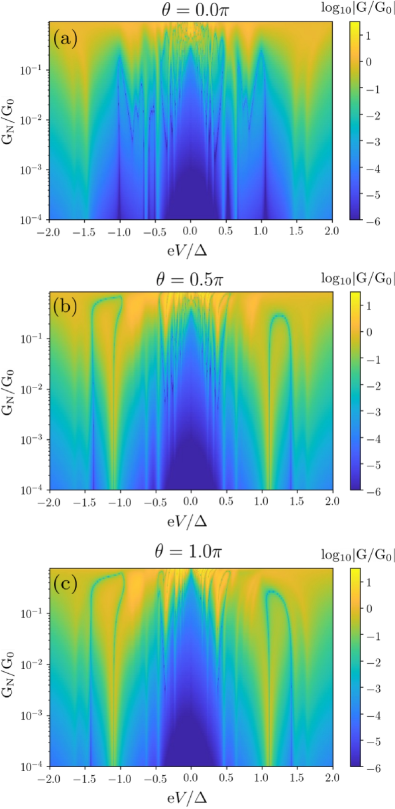
In this section we shall discuss the current-voltage characteristics beyond the tunnel regime with the goal to elucidate the different types of MARs that can take place in this system and to provide simple guidelines on how to identify the signatures of these processes. In Fig. 4 we illustrate the results for the differential conductance, , for parameter values similar to those of Fig. 3 and for a value of the hopping matrix element . Moreover, we shall focus on the case of zero temperature to simplify the discussion. The two panels correspond to the two limiting cases of parallel spins (), panel (a), and antiparallel spins (), panel (b). With the parameters chosen for this figure, the YSR bound states have energies and . For the parallel case of panel (a), we see the appearance of a rich structure, where the most pronounced conductance peaks appear at and . Obviously, these conductance peaks arise from single-quasiparticle tunneling connecting the YSR states of the tip and the substrate and the corresponding continuum density of states (DOS) outside the gap in the opposite electrode. These are first-order (in ) tunneling events that give the main contribution to the transport for parallel spins and low temperatures (they were already present in the example of Fig. 2(e)). Notice that the height of these peaks is different for positive and negative bias, which is due to the lack of electron-hole symmetry in this example. In the subgap region (), there is a series of conductance peaks. In particular, we observe peaks at and . This strongly suggests that these conductance peaks are due to second-order () Andreev reflections that involve a YSR state of one of the electrodes and the continuum DOS of the same lead. These processes also take place in the case of single-impurity junctions and, as it is known, they lead to peaks that depend on the bias polarity when there is no electron-hole symmetry, see Ref. Villas2020 and references therein. Additionally, one can also see several conductance peaks at and with . We attribute these peaks to processes that start or end in a YSR state and end or start at the residual DOS inside the gap due to the finite broadening parameters (). The peaks for correspond to single-quasiparticle tunneling, while those for correspond to the lowest-order Andreev reflection. This type of processes was discussed in Ref. Villas2020 in the context of single-impurity junctions and we shall not pay much attention to it in this work. It is also worth remarking that there is no negative differential conductance (NDC) in this case, i.e., there are no current peaks. Let us also clarify that thermal Shiba-Shiba tunneling discussed in the previous section does not show up in Fig. 4(a) because we are assuming zero temperature.
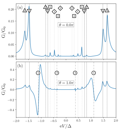
In the case of antiparallel spins, see Fig. 4(b), the new characteristics, compared to the parallel case, that appear in the differential conductance are NDC features at and at , which correspond to peaks in the current at those voltages. The first features are nothing else than the signature of the direct Shiba-Shiba tunneling discussed in the previous section, which are due to single-quasiparticle processes between the YSR states in both impurities. The values of the bias at which the second features appear strongly suggest that they originate from Andreev reflections (of third order in the tunneling probability) that start and end in YSR states in a different impurity. As we shall discuss in more detail below, these processes are forbidden in this example for because of the full spin polarization of the YSR states, but they are allowed for any and its probability is maximized for . This type of MAR processes, which we shall refer to as Shiba-Shiba MARs, has no analogue in the case of single-impurity junctions Villas2020 . Notice, in particular, that the NDC associated with these processes is a natural consequence of their resonant character. Notice also that in this case the features for positive and negative bias are different, which again can be traced back to the lack of electron-hole symmetry in this example.
.
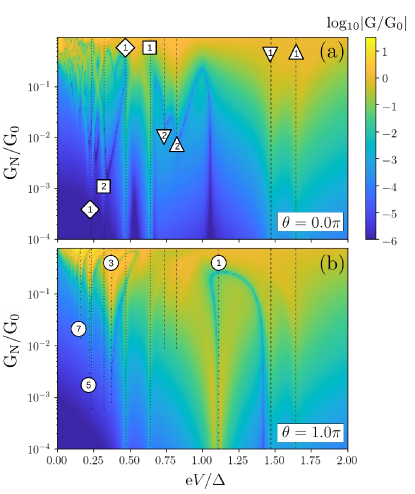
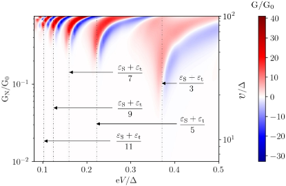
To get further insight into the origin of the subgap features, we present in Fig. 5 a systematic study of the evolution of the differential conductance as a function of the normal state conductance for the same parameters as in Fig. 4 (apart from the tunnel coupling), including also the results for an intermediate angle . Notice that for convenience we are plotting here the absolute value of the conductance in a logarithmic scale. With this choice, the NDC appears as a rapid alternation of bright and dark regions. The normal state conductance was varied in this case by changing the hopping and keeping fixed all the other parameters. In this figure, we can see the evolution of the conductance spectra as the junction transmission increases for different values of from the tunnel regime, where only single-quasiparticle tunneling processes contribute to the transport, to the case of relatively transparent junctions where MAR processes also contribute giving rise to a very rich subgap structure. To better understand these spectra, we have reproduced the results for and in Fig. 6 focusing on positive bias and we have included different vertical lines indicating the relevant energies discussed in the previous paragraphs. The labeling of these lines follows the convention explained in the caption of Fig. 4. The most important observation is the appearance for of several NDC features (corresponding to current peaks) at voltages with , which become more and more prominent as the normal state conductance increases. As explained above, the natural explanation for these features is the occurrence of a special type of MARs starting and ending in YSR states of a different impurity. On the other hand, irrespective of the value of , there is also a series of conductance peaks at and that can be attributed to MARs that involve a YSR in only one of the impurities.
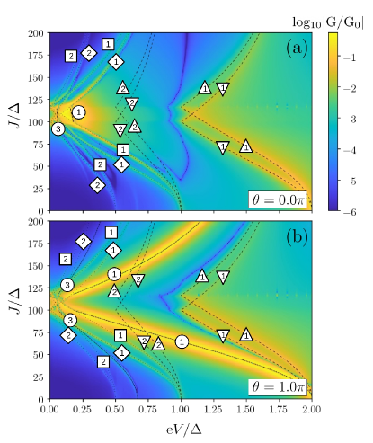
To further confirm our interpretation of the origin of the different subgap features, it is convenient to analyze how they shift when the energy of the YSR states is modified, for instance, by changing the exchange energy. This is what we illustrate in Fig. 7 where we show the evolution of the differential conductance with the exchange energy for the two extreme cases of and and for . To simplify the analysis we have assumed that both impurities have the same value of the exchange energy , which is changed simultaneously. Notice that we focus in this figure on positive voltages simply to make the different features clearly visible. As one can see, there are different running lines in these spectra whose dispersion with the exchange energy can be nicely described taken into account the -dependence of the energy of the YSR states in both impurities, see Eq. (12). This is illustrated in Fig. 7 with the inclusion of different dotted and dashed lines marking the relevant energies of these features. Thus, for instance, we have lines, labeled with circles, that indicate the values of the voltages with , which corresponds to the expected features of the Shiba-Shiba MARs. It may look surprising that some of the features appearing for have been assigned to these Shiba-Shiba MARs, see circles in panel (a). However, notice that in those regions, and because of the different values of , the spin of the ground state is different for both impurities and then the Shiba-Shiba MARs are allowed even for . The rest of the features in these spectra that can be attributed to either the MARs involving a single YSR state in one of the impurities or to the processes involving the residual DOS inside the gap region. This nicely confirms our interpretations above. Something else that is worth mentioning is the absence, also in the previous figures, of the standard subharmonic gap structure at with . This structure is due to conventional MARs that do not involve YSR states and take place between the continua of states in the leads Cuevas1996 ; Villas2020 . In regular situations with no impurities, these MARs give rise to the subharmonic gap structure, consisting of conductance peaks at , because of the BCS singularities at the gap edges. In our system, those MARs also take place, but the gap edge singularities are not present in the DOS of the impurities, which explains the absence of this conventional structure. In an actual experiment, one may have additional, non-magnetic channels for tunneling, see e.g. Ref. Huang2020b , and then this standard subgap structure can coexist with the one we are describing in this work.
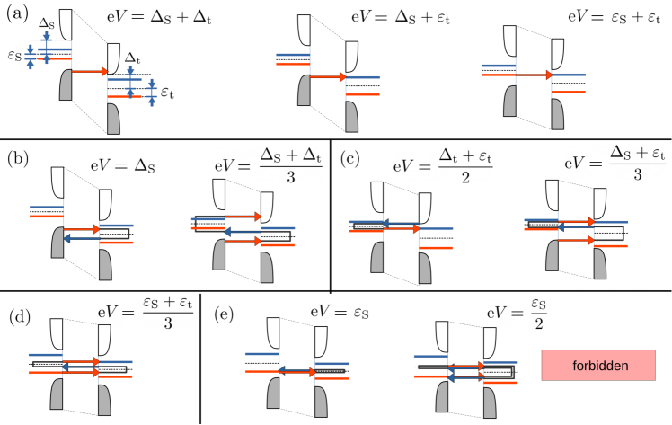
After the analysis of the previous results, we are now in position to summarize all the relevant tunneling processes that occur in our system, which are schematically shown in Fig. 8. In this figure, the diagrams display the DOS of the substrate and tip impurities featuring YSR states and we assume a positive bias. Notice, in particular, the absence of gap edge singularities, as discussed above. The first class of processes are the single-quasiparticle events shown in panel (a), which dominate the charge transport in the tunnel regime. We have three types within this class: (i) tunneling processes between the continua of states in both leads (left diagram) with a threshold voltage equal to , (ii) tunneling processes between a YSR state of one impurity and the continuum of states of the other electrode (middle diagram) with a threshold voltage equal to , and the direct Shiba-Shiba tunneling (right diagram) with a resonant voltage equal to . The first type does not produce any abrupt feature (because of the absence of gap edge singularities), the second one gives rise to a conductance peak at its threshold voltage, and the third one is responsible for the direct Shiba-Shiba current peak (with NDC) at its resonant bias. Of course, these processes have their thermal counterparts at sufficiently high temperature and, in particular, one can have thermally activated tunneling between the YSR at , as we discussed in Sec. III.
The second type of tunneling processes are the conventional MARs shown in Fig. 8(b) that do not involve any YSR state. As discussed above, these processes usually give rise to a series of conductance peaks at subharmonics of combinations of the gaps Ternes2006 , but in our case those features are not visible due to the absence of gap edge singularities. However, these MARs can give resonant contributions, where their probability is greatly enhanced, when during the cascade of reflections a quasiparticle hits the energy of a YSR state in one of the impurities. Thus, for instance, the probability of the second-order Andreev reflection in Fig. 8(b) is resonantly enhanced when . Thus, this Andreev reflection competes with the single-quasiparticle process connecting the continuum of states in the substrate impurity and the YSR state in the tip impurity, and it eventually dominates the conductance peak height at this bias when the junction transmission is sufficiently high. These resonant Andreev reflections take also place in the case of single-impurity junctions where the competition just mentioned has been discussed in great detail both experimentally and theoretically Ruby2015 ; Villas2020 .
A more interesting family of MARs is that described in Fig. 8(c) in which the process starts or ends in a YSR state of one of the impurities. Depending on whether the order of the MAR, , is even or odd, one can have two types of threshold voltages Holmqvist2014 : (i) with when is even and (ii) when is odd, where stands for the electrode different from . The even processes start and end in the same electrode, as in the left diagram in Fig. 8(c), while the odd processes start and end in the different electrodes, as in the right diagram in Fig. 8(c). These MARs mediated by a YSR state give rise to conductance peaks (with no NDC) at those threshold voltages, as we have illustrated above for the case of a junction with equal superconducting gaps.
Probably the most interesting processes are the MARs that start and end in the YSR states of the different impurities, see Fig. 8(d). These Shiba-Shiba MARs occur at voltages given by with and give rise to current peaks (with NDC) at those voltages. Obviously, as in the case of the direct Shiba-Shiba tunneling, the width of the current peaks depends on the broadening of the involved YSR states. To illustrate once more the signature of these peculiar processes, we show in Fig. 9 the differential conductance in linear scale (and no absolute value) for one of the examples that we have discussed above, but focusing on low bias and relatively high normal state conductance values. In this case, we have used a different color code for the conductance map to highlight the NDC. As one can see, there is a series of NDC features associated with these Shiba-Shiba MARs. It is also interesting to notice that those features (corresponding to current peaks) tend to shift to higher voltages as the normal transmission of the junction is increased. We attribute this to the fact that for those normal state conductance values the electronic coupling between the impurities is strong enough to renormalize the energies of the bound states. In other words, those shifts are a signature of the hybridization of the YSR states in the two impurities. This is an interesting issue that we shall address in detail in a forthcoming paper.
Finally, we want to mention the MARs shown in Fig. 8(e), which would start and end in a YSR bound state of the same impurity. In principle, these processes are energetically allowed and they could give rise to current peaks at () with . However, as discussed in Ref. Villas2020 , the fact that the YSR states are fully polarized makes them forbidden. Such MARs would require a bound state to have a finite DOS of both spin species, which is not the case for YSR states.
V Conclusions
In summary, motivated by the very recent experimental realization of the tunneling between YSR states, we have presented in this work a comprehensive theoretical study of the tunneling processes that can take place in a system composed of two magnetic impurities coupled to their respective superconducting electrodes. Our analysis is based on the use of a mean-field Anderson model to describe the magnetic impurities and the Keldysh formalism to compute the current-voltage characteristics. First, we have shown that our model naturally explains all the basic experimental observations reported so far Huang2020a , which concerns the tunnel regime. In this regime, the subgap current exhibits current peaks with very large negative differential conductance that are the result of direct and thermally activated tunneling of single quasiparticles between the YSR states in both impurities. More importantly, we have predicted that upon increasing the junction transmission, the current can exhibit an extremely rich structure in the gap region due to the occurrence of several families of multiple Andreev reflections. Most notably, we have shown that one can have Andreev reflections connecting the YSR bound states in different impurities and that they give rise to a series of current peaks at subgap voltages. These processes have no analogue in single-impurity junctions and they illustrate the new physics that appears when there are superconducting bound states with broken spin symmetry. In principle, the experimental system of Ref. Huang2020a is ideally suited to test the different predictions put forward in this work.
Acknowledgements.
The authors would like to thank Alfredo Levy Yeyati, Joachim Ankerhold, Ciprian Padurariu, and Björn Kubala for insightful discussions. A.V. and J.C.C. acknowledge funding from the Spanish Ministry of Economy and Competitiveness (MINECO) (contract No. FIS2017-84057-P). This work was funded in part by the ERC Consolidator Grant AbsoluteSpin (Grant No. 681164) and by the Center for Integrated Quantum Science and Technology (IQ). R.L.K., W.B., and G.R. acknowledge support by the DFG through SFB 767 and Grant No. RA 2810/1. J.C.C. also acknowledges support via the Mercator Program of the DFG in the frame of the SFB 767. †These authors contributed equally to this work.References
- (1) L. Yu, Bound state in superconductors with paramagnetic impurities, Acta Phys. Sin. 21, 75 (1965).
- (2) H. Shiba, Classical Spins in Superconductors, Prog. Theor. Phys. 40, 435 (1968).
- (3) A. I. Rusinov, Superconductivity near a paramagnetic impurity, Pis’Ma Zh. Eksp. Teor. Fiz. 9, 146 (1968) [JETP Lett. 9, 85 (1969)].
- (4) A. Yazdani, B. A. Jones, C. P. Lutz, M. F. Crommie, and D. M. Eigler, Probing the Local Effects of Magnetic Impurities on Superconductivity, Science 275, 1767 (1997).
- (5) S.-H. Ji, T. Zhang, Y.-S. Fu, X. Chen, X.-C. Ma, J. Li, W.-H. Duan, J.-F. Jia, and Q.-K. Xue, High-Resolution Scanning Tunneling Spectroscopy of Magnetic Impurity Induced Bound States in the Superconducting Gap of Pb Thin Films, Phys. Rev. Lett. 100, 226801 (2008).
- (6) K. J. Franke, G. Schulze, and J. I. Pascual, Competition of Superconducting Phenomena and Kondo Screening at the Nanoscale, Science 332, 940 (2011).
- (7) G. C. Ménard, S. Guissart, C. Brun, S. Pons, V. S. Stolyarov, F. Debontridder, M. V. Leclerc, E. Janod, L. Cario, D. Roditchev, P. Simon, and T. Cren, Coherent long-range magnetic bound states in a superconductor, Nat. Phys. 11, 1013 (2015).
- (8) M. Ruby, F. Pientka, Y. Peng, F. von Oppen, B. W. Heinrich, and K. J. Franke, Tunneling Processes into Localized Subgap States in Superconductors, Phys. Rev. Lett. 115, 087001 (2015).
- (9) N. Hatter, B. W. Heinrich, M. Ruby, J. I. Pascual, and K. J. Franke, Magnetic anisotropy in Shiba bound states across a quantum phase transition, Nat. Commun. 6, 8988 (2015).
- (10) M. Ruby, Y. Peng, F. von Oppen, B. W. Heinrich, and K. J. Franke, Orbital Picture of Yu-Shiba-Rusinov Multiplets, Phys. Rev. Lett. 117, 186801 (2016).
- (11) M. T. Randeria, B. E. Feldman, I. K. Drozdov, and A. Yazdani, Scanning Josephson spectroscopy on the atomic scale, Phys. Rev. B 93, 161115(R) (2016).
- (12) D. J. Choi, C. Rubio-Verdú, J. De Bruijckere, M. M. Ugeda, N. Lorente, and J. I. Pascual, Mapping the orbital structure of impurity bound states in a superconductor, Nat. Commun. 8, 15175 (2017).
- (13) L. Cornils, A. Kamlapure, L. Zhou, S. Pradhan, A. A. Khajetoorians, J. Fransson, J. Wiebe, and R. Wiesendanger, Spin-Resolved Spectroscopy of the Yu-Shiba-Rusinov States of Individual Atoms, Phys. Rev. Lett. 119, 197002 (2017).
- (14) N. Hatter, B. W. Heinrich, D. Rolf, and K. J. Franke, Scaling of Yu-Shiba-Rusinov energies in the weak-coupling Kondo regime, Nat. Commun. 8, 2016 (2017).
- (15) L. Farinacci, G. Ahmadi, G. Reecht, M. Ruby, N. Bogdanoff, O. Peters, B. W. Heinrich, F. von Oppen, and K. J. Franke, Tuning the Coupling of an Individual Magnetic Impurity to a Superconductor: Quantum Phase Transition and Transport, Phys. Rev. Lett. 121, 196803 (2018).
- (16) J. Brand, S. Gozdzik, N. Néel, J. L. Lado, J. Fernández-Rossier, and J. Kröger, Electron and Cooper-pair transport across a single magnetic molecule explored with a scanning tunneling microscope, Phys. Rev. B 97, 195429 (2018).
- (17) L. Malavolti, M. Briganti, M. Hänze, G. Serrano, I. Cimai, G. McMurtrie, E. Otero, P. Ohresser, F. Toi, M. Mannini, R. Sessoli, and S. Loth, Tunable Spin-Superconductor Coupling of Spin 1/2 Vanadyl Phthalocyanine Molecules, Nano Lett. 18, 7955 (2018).
- (18) S. Kezilebieke, R. Žitko, M. Dvorak, T. Ojanen, and P. Liljeroth, Observation of Coexistence of Yu-Shiba-Rusinov States and Spin-Flip Excitations, Nano Lett. 19, 4614 (2019).
- (19) J. Senkpiel, C. Rubio-Verdú, M. Etzkorn, R. Drost, L. M. Schoop, S. Dambach, C. Padurariu, B. Kubala, J. Ankerhold, C. R. Ast, and K. Kern, Robustness of Yu-Shiba-Rusinov resonances in the presence of a complex superconducting order parameter, Phys. Rev. B 100, 014502 (2019).
- (20) L. Schneider, M. Steinbrecher, L. Rózsa, J. Bouaziz, K. Palotás, M. dos Santos Dias, S. Lounis, J. Wiebe, and R. Wiesendanger, Magnetism and in-gap states of 3d transition metal atoms on superconducting Re, Quantum Mater. 4, 42 (2019).
- (21) E. Liebhaber, S. A. González, R. Baba, G. Reecht, B. W. Heinrich, S. Rohlf, K. Rossnagel, F. von Oppen, and K. J. Franke, Yu-Shiba-Rusinov States in the Charge-Density Modulated Superconductor NbSe2, Nano Lett. 20, 339 (2020).
- (22) H. Huang, R. Drost, J. Senkpiel, C. Padurariu, B. Kubala, A. Levy Yeyati, J. C. Cuevas, J. Ankerhold, K. Kern, C. R. Ast, Quantum phase transitions and the role of impurity-substrate hybridization in Yu-Shiba-Rusinov states, Commun. Phys. 3, 199 (2020).
- (23) A. Odobesko, D. Di Sante, A. Kowalski, S. Wilfert, F. Friedrich, R. Thomale, G. Sangiovanni, and M. Bode, Observation of tunable single-atom Yu-Shiba-Rusinov states, Phys. Rev. B 102, 174504 (2020).
- (24) B. W. Heinrich, J. I. Pascual, and K. J. Franke, Single magnetic adsorbates on s-wave superconductors, Prog. Surf. Sci. 93, 1 (2018).
- (25) S. Nadj-Perge, I. K. Drozdov, J. Li, H. Chen, S. Jeon, J. Seo, A. H. MacDonald, B. A. Bernevig, A. Yazdani, Observation of Majorana Fermions in Ferromagnetic Atomic Chains on a Superconductor, Science 346, 602 (2014).
- (26) M. Ruby, F. Pientka, Y. Peng, F. von Oppen, B. W. Heinrich, K. J. Franke, End States and Subgap Structure in Proximity-Coupled Chains of Magnetic Adatoms, Phys. Rev. Lett. 115, 197204 (2015).
- (27) S. Kezilebieke, M. Dvorak, T. Ojanen, P. Liljeroth, Coupled Yu-Shiba-Rusinov states in molecular dimers on NbSe2, Nano Lett. 18, 2311 (2018).
- (28) M. Ruby, B. W. Heinrich, Y. Peng, F. von Oppen, K. J. Franke, Exploring a Proximity-Coupled Co Chain on Pb(110) as a Possible Majorana Platform, Nano Lett. 17, 4473 (2017).
- (29) M. Ruby, B. W. Heinrich, Y Peng, F. von Oppen, K. J. Franke, Wave-Function Hybridization in Yu-Shiba-Rusinov Dimers, Phys. Rev. Lett. 120, 156803 (2018).
- (30) H. Huang, C. Padurariu, J. Senkpiel, R. Drost, A. Levy Yeyati, J. C. Cuevas, B. Kubala, J. Ankerhold, K. Kern, C. R. Ast, Tunneling dynamics between superconducting bound states at the atomic limit, Nat. Phys. 16, 1227 (2020).
- (31) H. Huang, J. Senkpiel, C. Padurariu, R. Drost, A. Villas, R. L. Klees, A. Levy Yeyati, J. C. Cuevas, B. Kubala, J. Ankerhold, K. Kern, C. R. Ast, Spin-dependent tunneling between individual superconducting bound states, Phys. Rev. Research. 3, L032008 (2021).
- (32) J. Linder and J. W. A. Robinson, Superconducting spintronics, Nat. Phys. 11, 307 (2015).
- (33) M. Eschrig, Spin-polarized supercurrents for spintronics: a review of current progress, Rep. Prog. Phys. 78, 104501 (2015).
- (34) C. Holmqvist, W. Belzig, and M. Fogelström, Non-equilibrium charge and spin transport in superconducting-ferromagnetic-superconducting point contacts, Phil. Trans. R. Soc. A 376, 20150229 (2018).
- (35) L. Schneider, P. Beck, J. Wiebe, R. Wiesendanger, Atomic-scale spin-polarization maps using functionalized superconducting probes, Sci. Adv. 7, eabd7302 (2021).
- (36) D. Averin and D. Bardas, AC Josephson Effect in a Single Quantum Channel, Phys. Rev. Lett. 75, 1831 (1995).
- (37) J. C. Cuevas, A. Martín-Rodero, and A. Levy Yeyati, Hamiltonian approach to the transport properties of superconducting quantum point contacts, Phys. Rev. B 54, 7366 (1996).
- (38) E. Scheer, P. Joyez, D. Esteve, C. Urbina, and M. H. Devoret, Conduction Channel Transmissions of Atomic-Size Aluminum Contacts, Phys. Rev. Lett. 78, 3535 (1997).
- (39) E. Scheer, N. Agraït, J. C. Cuevas, A. Levy Yeyati, B. Ludoph, A. Martin-Rodero, G. Rubio Bollinger, J. M. van Ruitenbeek, and C. Urbina, The signature of chemical valence in the electrical conduction through a single-atom contact, Nature (London) 394, 154 (1998).
- (40) A. Villas, R. L. Klees, H. Huang, C. R. Ast, G. Rastelli, W. Belzig, J. C. Cuevas, Interplay between Yu-Shiba-Rusinov states and multiple Andreev reflections, Phys. Rev. B 101, 235445 (2020).
- (41) A. Martín-Rodero and A. Levy Yeyati, Josephson and Andreev transport through quantum dots, Adv. Phys. 60, 899 (2011).
- (42) A. Martín-Rodero and A. Levy Yeyati, The Andreev states of a superconducting quantum dot: mean field versus exact numerical results, J. Phys.: Condens. Matter. 24, 385303 (2012).
- (43) M. Ternes, W. D. Schneider, J. C. Cuevas, C. P. Lutz, C. F. Hirjibehedin, and A. J. Heinrich, Novel subgap structure in asymmetric superconducting tunnel junctions, Phys. Rev. B 74, 132501 (2006).
- (44) C. Holmqvist, M. Fogelström, and W. Belzig, Spin-polarized Shapiro steps and spin-precession-assisted multiple Andreev reflection, Phys. Rev. B 90, 014516 (2014).