Quantum Sensing of Single Phonons via Phonon Drag in Two-Dimensional Materials
Abstract
The capacity to electrically detect phonons, ultimately at the single-phonon limit, is a key requirement for many schemes for phonon-based quantum computing, so-called quantum phononics. Here, we predict that by exploiting the strong coupling of their electrons to surface-polar phonons, van der Waals heterostructures can offer a suitable platform for phonon sensing, capable of resolving energy transfer at the single-phonon level. The geometry we consider is one in which a drag momentum is exerted on electrons in a graphene layer, by a single out-of-equilibrium phonon in a dielectric layer of hexagonal boron nitride, giving rise to a measurable induced voltage (). Our numerical solution of the Boltzmann Transport Equation shows that this drag voltage can reach a level of a few hundred microvolts per phonon, well above experimental detection limits. Furthermore, we predict that should be highly insensitive to the mobility of carriers in the graphene layer and to increasing the temperature to at least 300 K, offering the potential of a versatile material platform for single-phonon sensing.
I Introduction
A key requirement of quantum computing is the on-demand generation and coherent manipulation of quantum states. From a practical perspective, the ability to implement these operations using chip-scale integrated circuits is highly desired, as it would open up the capability to fully leverage the many advantages of the mature microelectronics industry. However, a fundamental barrier to solid-state quantum computing has long been understood to arise from the role of phonons. At nonzero temperatures, these bosonic modes can be occupied with broad distributions of energy and momentum, allowing them to function as an efficient “bath” whose many degrees of freedom can efficiently randomize (or decohere) quantum information. Although the manner in which a densely populated phonon bath destroys quantum coherence has long been understood, it has only recently become appreciated that phonons may instead provide an effective means of transmitting quantum information when excited coherently in sufficiently small numbers [1, 2, 3, 4, 5, 6, 7]. The strong coupling of phonons to other quasiparticles (especially electrons or photons) makes them well suited to this task. Furthermore, the physical patterning of bulk crystals can be exploited to implement phononic crystals [8, 9, 10], in strong analogy with their photonic counterparts, or to realize resonant structures that can be selectively coupled to single quanta [11, 12]. Various schemes for phonon-mediated quantum transduction have been proposed [13, 14, 15, 16, 17, 18, 19], and phonons have also been suggested as a means of mediating quantum entanglement [20]. In other work, the development of phononic circuits for applications in quantum sensing and signal processing has been emphasized [21, 22]. Stark shift measurements as a function of the number of phonons [23] have been demonstrated and are based on the real part of the electron-phonon self-energy. Other phonon detection schemes use optomechanical response [24], including the famous LIGO gravitational wave interferometer [25]. In contrast to these different approaches, a phonon-drag detection scheme is proposed that utilizes a 2D material platform and which takes advantage of the imaginary part of the self-energy, leading to high detection efficiency and simplicity of implementation.
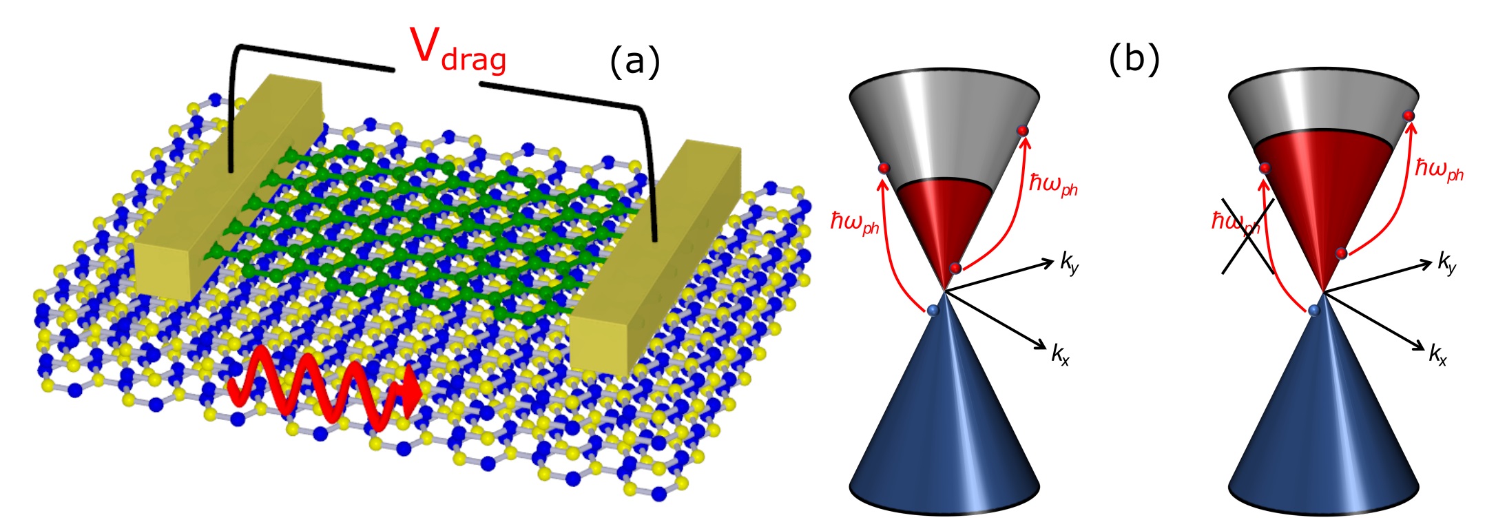
For phononic control to approach the levels of sophistication that have already been achieved for electrons and photons, there are a number of critical issues that need to be addressed. Key among these is the need to detect phonons in real-time in an electrical measurement, using approaches that can ultimately be scaled to the limit of single-phonon resolution. In this work, we propose and predict the quantitative performance of a single-phonon detector that is implemented in a heterostructure of monolayer (or AB-stacked bilayer) graphene and multilayer hexagonal boron nitride (hBN). It has been known for four decades that remote phonon scattering hinders the mobility of semiconductors grown on polar substrates, in which ionic motion generates an electric field that extends into the semiconductor [26, 27]. In this work, we propose to make use of remote phonon scattering to implement phonon detectors. Two-dimensional materials such as graphene have recently attracted increasing interest for application in quantum computing technology [28]. When choosing the particular geometry of Fig. 1a, we are motivated by the fact that hBN is a notable phononic material, having branches of phonon polariton (near 100 meV and over the range from 175 – 200 meV) that exhibit a hyperbolic character due to the strong optical anisotropy. This allows thin slabs of this material to function as efficient waveguides for propagating phonons [29, 30, 31], a characteristic that has been exploited [32] to achieve rapid cooling of the hot carrier in graphene / hBN-based transistors. At the same time, the presence of the tunable, high-conductivity electron gas in graphene renders it well suited for the drag-based detection of phonons in the hBN. To demonstrate this, we consider a situation in which a single surface polar phonon (SPP) is excited in the hBN and travels along the heterostructure while interacting with electrons in the graphene layer. This process leads to the development of the drag-based voltage shown in Fig. 1a.
In a heterostructure formed between graphene and monolayer hBN, the inherent 2D nature of the materials gives rise to hybrid plasmon-phonon polaritons that propagate parallel to the plane of their interface. However, the situation is very different when graphene is deposited in thicker layers of hBN (in the range of 1 – 100 nm), in which the phonon polaritons exhibit a hyperbolic character, capable of propagation with large energy and momentum losses. Optical phonons injected into hBN will initially propagate with a ray-like character before decaying via crystal anharmonicity over a characteristic distance of a few tens of nanometers, allowing the formation of long-lived [33, 34] SPPs at the boundary between the hBN and graphene layers. Our calculated results demonstrate that the drag voltage that develops in such structures is on the scale of a few hundred microvolts for a device one micrometer wide, well above the detection limit in typical experimental setups.
II Modeling approach
The interplay of charge carrier flow with phonon transport (and vice versa) has a long history of discussion in thermoelectrics [35, 36, 37]. At the same time, interest in the problem of phonon drag has been revived in the context of low-dimensional materials [38, 39, 40, 41, 42, 43]. We assume a quasiparticle picture of electrons and phonons in our study, employing the Boltzmann transport formalism in our calculations [44]:
| (1) |
Here, is the distribution function of electrons in momentum space, is the electron wavevector, including the band index, is the external electric field that acts as the driving force, is the group velocity of electrons and is the Planck constant. The terms on the right-hand side of the equation describe collision integrals due to electron-phonon () and electron-impurity () scattering.
The collision integral for electron-phonon scattering is given by:
| (2) |
In this equation, is the number of occupied phonon modes with momentum and energy , is the electron energy, and the -function ensures energy conservation. is the coupling constant of the e-ph interaction. The details of the electron-SPP scattering are given in Appendix A and intrinsic electron-phonon interactions are taken into account following Ref. [45].
The collision integral for Coulomb impurity scattering is added using a standard procedure [46, 47, 48, 49]. Unless stated otherwise, we choose the impurity concentration to give a typical mobility of cm2/Vs for the graphene devices.
The problem we consider is one in which the phonon systems of both materials are initially in thermal equilibrium and in which we then assume that a single SPP (of wavevector in direction ) is excited in the hBN layer. As a result of this, the distribution function in Eq. (1) changes by an amount , leading to an excess current density . We define the resulting drag voltage via:
| (3) |
where is the electrical conductivity and and are the width and length of the device, respectively. In simulations, we use a supercell approach such that the -point mesh of the Brillouin zone defines the corresponding area of the device in real space, i.e., , where is the area of the primitive unit cell. According to Eq. (II), the drag voltage is inversely proportional to the width of the conducting graphene channel. In the analysis that follows, we therefore report the results of the product . It should be noted that our choice to characterize the responsivity of the phonon sensor in terms of the drag voltage leads to a counterintuitive conclusion that the responsivity is independent of the quality of the graphene sample and of the strength of the impurity scattering (see discussion below). This result is a consequence of the form of Eq. (II), in which the caused by an out-of-equilibrium phonon is proportional to the electrical conductivity, leading to being nearly independent of mobility. The phonon-induced current is certainly sensitive to the quality of graphene, however.
III Results and Discussion
Through a process of absorption, the out-of-equilibrium SPP excites an initial electron into a higher energy state (see Fig. 1). The conservation of energy and momentum requirements impose a dependence of on the SPP wavevector and the Fermi energy in the graphene. Fig. 1 illustrates two possible electron excitations that can arise from absorption of the out-of-equilibrium phonon: an inter-band transition of an electron from the valence- to the conduction-band, as shown in Fig. 1a, or an intra-band transition between two states in the conduction-band, as shown in Figs. 1a and 1b. Energy conservation prohibits interband transitions once the Fermi level is larger than the SPP energy i.e., in monolayer or bilayer graphene.
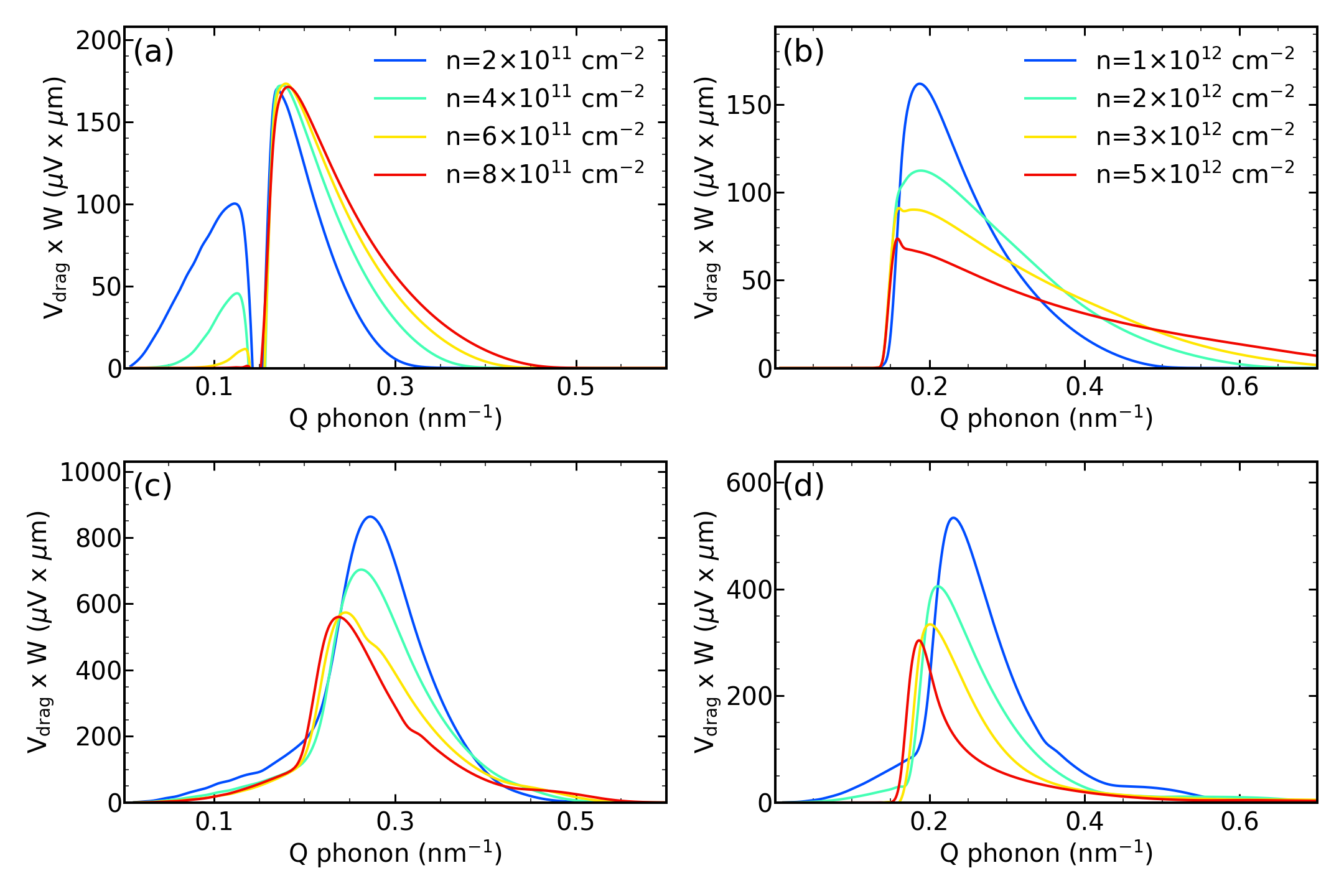
In Fig. 2 we plot the variation of as a function of the SPP wavevector, for various carrier densities in both the monolayer (Figs. 2a and b) and bilayer graphene (Figs. 2c and d). In the monolayer case, the drag signal exhibits two distinct peaks, the first of which, at small wavevector, is associated with inter-band excitation of electrons from the valence- to the conduction-band. The wavevectors at which the peaks in the drag signal occur reflect the details of the phase space for scattering, which is goverened by conservation of energy and momentum and the Pauli blocking principle. The amplitude of these peaks is determined by the strength of the electron-phonon matrix elements. The finite temperature primarily introduces thermal smearing of the electronic states. As indicated by the schematic of Fig. 1, these transitions are able to satisfy energy and momentum conservation laws at small SPP wavevector. They are cut-off at wavevectors greater than nm-1, where m/s is the Fermi velocity in the monolayer and meV is the phonon energy, see Appendix A. The inter-band transitions are to be contrasted with those responsible for the second peak in the drag signal, seen at larger wavevectors, which instead involve intra-band processes.
Turning next to the results for bilayer graphene (Figs. 2c and 2d), we see that the small-wavevector peak found in the monolayer case is replaced now by a shoulder-like feature for wavevectors , where nm-1, is effective mass in bilayer graphene [50], and is free-electron mass. The absence of the inter-band drag peak at small wavevectors is a consequence of the reduced phase space available for electron scattering in the parabolic bands of the bilayer. One can estimate the carrier density at which the feature in the drag signal due to inter-band transitions should be suppressed, in monolayer or bilayer graphene, as cm-2 and cm-2, respectively. These estimates are consistent with the trends indicated in Fig. 2.
As doping increases in monolayer graphene, the wavevector range over which phonon detection can be achieved increases, as reflected by the increase in the width of the peak of the higher moment in Fig. 2b. Similar phase-space arguments apply to bilayer graphene. One can estimate a wavevector cut-off for the intra-band transitions according to in monolayer graphene and in bilayer graphene, where is the Fermi wavevector and we have used an effective Fermi velocity in bilayer graphene. The largest carrier density of cm-2 used in Figs. 2b and 2d translates to corresponding estimates of 0.95 nm-1. However, the detection signal dies at smaller wavevectors of about nm-1 in the case of bilayer graphene, which is due to the decay of the electron-SPP matrix element at large wavevectors, as discussed in Appendix A and illustrated in Figs. 3c and 3d.
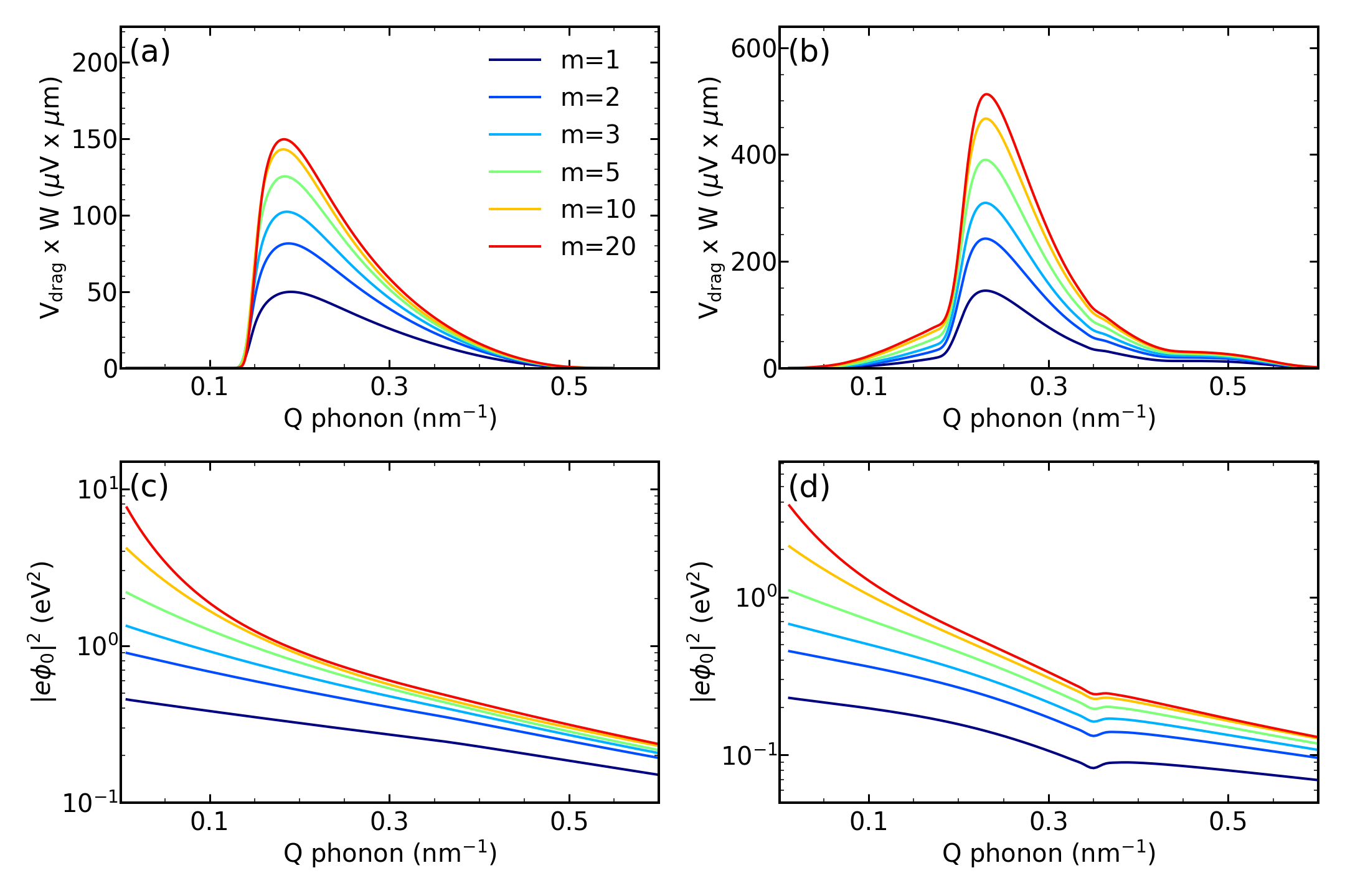
To provide insight into the dependence of the drag signal on the thickness of the hBN, we calculated (at a fixed carrier density cm-2) for several values of . The results are shown in Figs. 3a and 3b, for monolayer and bilayer graphene, respectively. As the number of layers is reduced, the electric field associated with the SPP also decreases. However, this variation is relatively weak, and is reduced by only a factor of three relative to the bulk case, by the time that the single layer limit is reached. Conversely, as the hBN thickness increases from the single-layer limit, the drag signal saturates once the number of hBN layers reaches around twenty.
To better understand the -vector dependence of the drag voltage at large momenta, we note that the electron-SPP coupling is Coulombic in nature. According to Eq. (16), the Fourier transform of this coupling has a strong momentum dependence. In Figs. 3c and 3d, we plot the scaling of the electron-SPP scattering potential as a function of the phonon wavevector to vary the number of hBN layers. The momentum dependence of reported here is a consequence of the product of the electron-SPP coupling and the phase space available for electron excitation due to the non-equilibrium phonon.
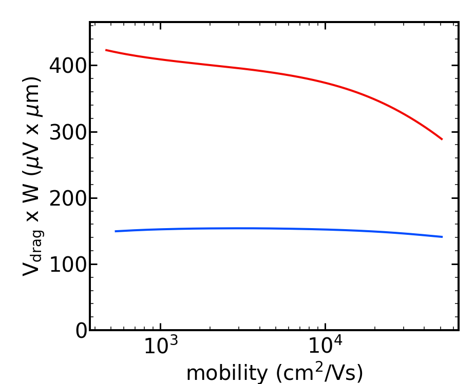
The trend apparent in Figs. 2b and 2d, for the amplitude of the higher moment peak to decrease with increasing carrier density, can be attributed to the dependence of electrical conductivity on density, i.e., , where is the carrier mobility and is the effective scattering time. According to Eq. (II), is inversely proportional to , which accounts for the reduction mentioned above of with increasing density. At the same time, one should keep in mind that the increase in the distribution function () due to the excitation of the single out-of-equilibrium phonon is proportional to . This means that the influence of impurity scattering on the drag voltage should be relatively weak. In fact, in Fig. 4 we show that is almost independent of , whose value is largely determined by the concentration of impurities.
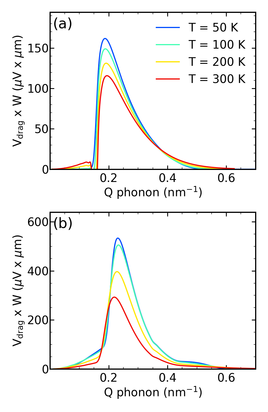
We have also explored the dependence of the drag signal on the equilibrium lattice temperature. The influence of this parameter is illustrated in Fig. 5, for both monolayer and bilayer graphene. (The calculations are performed for a representative density cm-2, and for ). Due to the large SPP energy (100 meV), is reduced by only about 30% in monolayer graphene (and 50% in bilayer graphene), when the temperature increases from 50 to 300 K. This robust character opens up the possibility of realizing single-phonon detectors that are capable of functioning at room temperature.
When considering schemes for single-phonon detection, it is important to keep in mind the fact that phonons have a finite lifetime due to phonon-phonon decay, and a transit time that is determined by the transistor size and the phonon velocity . For a field-effect transistor with channel length m, the transient time can be estimated as ns, setting an upper bound for the limited lifetime of anahrmonic decay . Transient effects can therefore be modeled by the Boltzmann transport equation as follows:
| (4) |
where, without loss of generality, we have used the relaxation time approximation to describe electron-impurity scattering in terms of an effective scattering time . The NQ subscript for the collision integral denotes the contribution to electron scattering due to the single out-of-equilibrium phonon. The solution of Eq. (5) is given by:
| (5) |
where is the steady-state solution of Eq. (1). According to Eq. (II), the drag voltage will be reduced by a factor of and will have the same exponential time dependence as appears in Eq. (5). The steady-state solution for the drag voltage corresponds to the limit in the transient solution:
| (6) |
where is given by Eq. (II) and reported in Figs. 2-5. While counter-intuitive, Eq. (6) suggests that lower-mobility graphene, with shorter scattering time, should perform better in measuring transient phonon-drag voltage signals.
An important parameter for sensor characterization is the noise equivalent power (NEP), which characterizes the signal-to-noise ratio of the phonon detectors. Phonons follow Bose-Einstein statistics, meaning that the noise considerations relevant to single-photon detectors should also be applicable to the single-phonon detector proposed here. Following Ref. [51], we can estimate the NEP due to the Johnson-Nyquist noise contribution as a ratio of Johnson noise and voltage responsivity, where is the resistance of the device. The voltage responsivity can be estimated as , where the transient time ns. Using realistic device parameters: micron, cm-2, cm2/Vs, and a typical V, we thus estimate the NEP to be 0.16 fWHz-1/2.
Fluctuations in the phonon distribution are not taken into account in our Boltzmann Transport approach, and any temperature dependencies arises from the thermal smearing of the electron distribution function. Fluctuations in the phonon population are known to cause noise in conductivity [52]. We emphasize that here we consider phonon drag due to a single SPP phonon in h-BN, a mode whose thermal population is very small at room temperatures.
IV Conclusions
In conclusion, we have shown theoretically that the phonon-drag effect in two-dimensional layered materials can enable the sensitive, quantum detection of phonons, with the potential of operation down to the single-phonon level. The strong coupling between electrons and SPPs in the coupled conductive and dielectric layers is predicted to give rise to a drag voltage as large as a few hundred microvolts per phonon, well above the experimental detection limit. The drag voltage is, moreover, predicted to be relatively insensitive to variation in the mobility of the graphene layer and should exhibit only a weak temperature dependence. These characteristics relax the need for high-mobility detectors that operate at ultralow temperatures. By varying the Fermi level in graphene using a suitable gate, the phonon detectors described here should act as efficient energy-resolved phonon sensors, since momentum conservation laws set stringent requirements on the range of phonon wavevectors that can be detected. Our study provides further evidence of the outstanding potential of 2D heterostructures for use in quantum information science and quantum sensing [28].
Acknowledgements.
This material is based upon work supported by the Air Force Office of Scientific Research under award number FA9550-22-1-0312.Appendix A Electron-SPP matrix element
To determine the electron-SPP coupling, we solve Maxwell’s equation for the spatial dependence of the electric potential due to the SPP, using the following ansatz [27]:
| (7) |
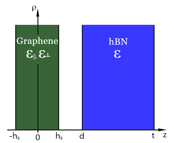
Here, and are the two-dimensional phonon wave vector and the spatial coordinate, respectively, and is the phonon frequency. In isotropic materials, the Poisson equation requires with . However, in an anisotropic dielectric . Following Ref. [45], we treat monolayer (bilayer) graphene as a dielectric layer of thickness , as shown in Fig. 6, where Å( Å) for monolayer (bilayer) and accounts for the size of the electron cloud of the orbitals of carbon atoms. The thickness hBN is placed at the van der Waals distance Å( Å) for monolayer (bilayer) graphene. Perpendicular to the plane, we choose the dielectric constant , as appropriate for the interface of bilayer graphene [53]. Within the plane, we choose a static dielectric function , where , is the polarization function from the Random Phase Approximation, and we use the zero temperature limit [46, 47].
The solution for in Eq. (7) has the form:
| (8) |
The coefficients and the dispersion relation for the SPPs are found using the boundary conditions , at , , and , where the superscripts “” and “” indicate functions to the right and left of the boundaries, respectively.
The dielectric function hBN is given by:
| (9) |
where , , and meV [54, 55]. (We omit the higher energy SPP branch at 200 meV.) The resulting solution for the SPP frequency is given by:
| (10) |
where is the solution of the dispersion relation. To find the coefficients in Eq. (8) and the dispersion relation, we define and introduce the following variables:
| (11) |
The coefficients are given by the following:
| (12) |
The dispersion relation is obtained from the condition for the coefficient :
| (13) |
After rearranging Eqs. (13) and (12), we find that , where is given by:
| (14) |
The two different solutions of are due to the two surfaces of the finite thickness hBN.
To find the form of the SPP potential that interacts with electrons in graphene i.e., according to Eq. (8), we apply the normalization condition [56, 57]:
| (15) |
which allows us to solve for the magnitude of the coefficients . In Eq. (15), , is the sample area, is the unit cell area, and is the number of k points. Finally, the e-SPP coupling constant can be obtained as
| (16) |
Here, is a single particle wave function and the inner product in Eq. (16) should be understood as corresponding to the wave function overlap in a primitive unit cell, not the entire sample. In the low-energy model, the wavefunction overlap between two states in the conduction band is for monolayer graphene, and for bilayer, where is the angle between the two wavevectors and [58].
We note that the unscreened potential can be obtained by setting in the above equations and that the two SPP branches become degenerate in the absence of screening and infinitely thick hBN i.e., and . However, in this case, the electron-SPP coupling for each phonon branch would be half of the conventional coupling for semi-infinite hBN [55, 59]. SPPs in the above solution form symmetric and antisymmetric linear combinations of two localized phonons at the two surfaces, with each of them contributing half of the coupling to electrons. The screening of graphene breaks the symmetry and the SPP branch, which corresponds to the larger root in Eq. (14) (or smaller SPP energy), gives the dominant electron-SPP coupling. At the same time, the smaller root of in Eq. (14) gives negligible contribution at large values of and is consistently below 25% throughout the range of values of and reported in this study. To address that artifact of the model, which does not include losses in hBN, we use the larger root for in Eq. (14) for the phonon energy, and contributions from both branches of SPP for the electron-SPP coupling. Note that in the limit of small , and according to Eq. (10) , whereas in the opposite limit , and the conventional result for the SPP frequency corresponding to semi-infinite hBN and unscreened potential are obtained: . Consequently, the overall SPP dispersion width, meV, is much smaller than the typical SPP energy meV.
References
- Chu et al. [2018] Y. Chu, P. Kharel, T. Yoon, L. Frunzio, P. T. Rakich, and R. J. Schoelkopf, Creation and control of multi-phonon fock states in a bulk acoustic-wave resonator, Nature 563, 666 (2018).
- Gustafsson et al. [2014] M. V. Gustafsson, T. Aref, A. F. Kockum, M. K. Ekström, G. Johansson, and P. Delsing, Propagating phonons coupled to an artificial atom, Science 346, 207 (2014).
- Manenti et al. [2017a] R. Manenti, A. F. Kockum, A. Patterson, T. Behrle, J. Rahamim, G. Tancredi, F. Nori, and P. J. Leek, Circuit quantum acoustodynamics with surface acoustic waves, Nature communications 8, 1 (2017a).
- Noguchi et al. [2017] A. Noguchi, R. Yamazaki, Y. Tabuchi, and Y. Nakamura, Qubit-assisted transduction for a detection of surface acoustic waves near the quantum limit, Physical Review Letters 119, 180505 (2017).
- Bolgar et al. [2018] A. N. Bolgar, J. I. Zotova, D. D. Kirichenko, I. S. Besedin, A. V. Semenov, R. S. Shaikhaidarov, and O. V. Astafiev, Quantum regime of a two-dimensional phonon cavity, Physical Review Letters 120, 223603 (2018).
- Moores et al. [2018] B. A. Moores, L. R. Sletten, J. J. Viennot, and K. Lehnert, Cavity quantum acoustic device in the multimode strong coupling regime, Physical review letters 120, 227701 (2018).
- Satzinger et al. [2018] K. J. Satzinger, Y. Zhong, H.-S. Chang, G. A. Peairs, A. Bienfait, M.-H. Chou, A. Cleland, C. R. Conner, É. Dumur, J. Grebel, et al., Quantum control of surface acoustic-wave phonons, Nature 563, 661 (2018).
- Schuetz et al. [2015] M. Schuetz, E. Kessler, G. Giedke, L. Vandersypen, M. Lukin, and J. Cirac, Universal quantum transducers based on surface acoustic waves, Phys Rev X 5, 031031 (2015).
- Kurizki et al. [2015] G. Kurizki, P. Bertet, Y. Kubo, K. Mølmer, D. Petrosyan, P. Rabl, and J. Schmiedmayer, Quantum technologies with hybrid systems, Proceedings of the National Academy of Sciences 112, 3866 (2015).
- Reinke and El-Kady [2016] C. M. Reinke and I. El-Kady, Phonon-based scalable platform for chip-scale quantum computing, AIP Advances 6, 122002 (2016).
- Poot and van der Zant [2012] M. Poot and H. S. van der Zant, Mechanical systems in the quantum regime, Physics Reports 511, 273 (2012).
- Barfuss et al. [2015] A. Barfuss, J. Teissier, E. Neu, A. Nunnenkamp, and P. Maletinsky, Strong mechanical driving of a single electron spin, Nature Physics 11, 820 (2015).
- Safavi-Naeini and Painter [2011] A. H. Safavi-Naeini and O. Painter, Proposal for an optomechanical traveling wave phonon–photon translator, New Journal of Physics 13, 013017 (2011).
- Lemonde et al. [2018] M.-A. Lemonde, S. Meesala, A. Sipahigil, M. Schuetz, M. Lukin, M. Loncar, and P. Rabl, Phonon networks with silicon-vacancy centers in diamond waveguides, Physical review letters 120, 213603 (2018).
- Weber et al. [2010] J. Weber, W. Koehl, J. Varley, A. Janotti, B. Buckley, C. Van de Walle, and D. D. Awschalom, Quantum computing with defects, Proceedings of the National Academy of Sciences 107, 8513 (2010).
- Chen et al. [2018] H. Y. Chen, E. MacQuarrie, and G. D. Fuchs, Orbital state manipulation of a diamond nitrogen-vacancy center using a mechanical resonator, Physical review letters 120, 167401 (2018).
- Chen et al. [2019] H. Chen, N. F. Opondo, B. Jiang, E. R. MacQuarrie, R. S. Daveau, S. A. Bhave, and G. D. Fuchs, Engineering electron–phonon coupling of quantum defects to a semiconfocal acoustic resonator, Nano letters 19, 7021 (2019).
- Vermersch et al. [2017] B. Vermersch, P.-O. Guimond, H. Pichler, and P. Zoller, Quantum state transfer via noisy photonic and phononic waveguides, Physical review letters 118, 133601 (2017).
- Kitzman et al. [2022] J. M. Kitzman, J. R. Lane, C. Undershute, P. M. Harrington, N. R. Beysengulov, C. A. Mikolas, K. W. Murch, and J. Pollanen, Quantum acoustic bath engineering, arXiv:2208.07423 (2022).
- Hucul et al. [2015] D. Hucul, I. V. Inlek, G. Vittorini, C. Crocker, S. Debnath, S. M. Clark, and C. Monroe, Modular entanglement of atomic qubits using photons and phonons, Nature Physics 11, 37 (2015).
- Aref et al. [2016] T. Aref, P. Delsing, M. K. Ekström, A. F. Kockum, M. V. Gustafsson, G. Johansson, P. J. Leek, E. Magnusson, and R. Manenti, Quantum acoustics with surface acoustic waves, in Superconducting Devices in Quantum Optics, edited by R. H. Hadfield and G. Johansson (Springer International Publishing, Cham, 2016) pp. 217–244.
- Safavi-Naeini et al. [2019] A. H. Safavi-Naeini, D. Van Thourhout, R. Baets, and R. Van Laer, Controlling phonons and photons at the wavelength scale: integrated photonics meets integrated phononics, Optica 6, 213 (2019).
- Manenti et al. [2017b] R. Manenti, A. F. Kockum, A. Patterson, T. Behrle, J. Rahamim, G. Tancredi, F. Nori, and P. J. Leek, Circuit quantum acoustodynamics with surface acoustic waves, Nature Communications 8, 975 (2017b).
- Li et al. [2007] M. Li, H. X. Tang, and M. L. Roukes, Ultra-sensitive nems-based cantilevers for sensing, scanned probe and very high-frequency applications, Nature Nanotechnology 2, 114 (2007).
- Barish and Weiss [1999] B. C. Barish and R. Weiss, Ligo and the detection of gravitational waves, Physics Today 52, 44 (1999).
- Hess and Vogl [1979] K. Hess and P. Vogl, Remote polar phonon scattering in silicon inversion layers, Solid State Communications 30, 797 (1979).
- Fischetti et al. [2001] M. V. Fischetti, D. A. Neumayer, and E. A. Cartier, Effective electron mobility in si inversion layers in metal–oxide–semiconductor systems with a high- insulator: The role of remote phonon scattering, Journal of Applied Physics 90, 4587 (2001).
- Liu and Hersam [2019] X. Liu and M. C. Hersam, 2d materials for quantum information science, Nature Reviews Materials 4, 669 (2019).
- Dai et al. [2015] S. Dai, Q. Ma, M. Liu, T. Andersen, Z. Fei, M. Goldflam, M. Wagner, K. Watanabe, T. Taniguchi, M. Thiemens, et al., Graphene on hexagonal boron nitride as a tunable hyperbolic metamaterial, Nature nanotechnology 10, 682 (2015).
- Principi et al. [2017] A. Principi, M. B. Lundeberg, N. C. Hesp, K.-J. Tielrooij, F. H. Koppens, and M. Polini, Super-planckian electron cooling in a van der waals stack, Physical review letters 118, 126804 (2017).
- Low et al. [2017] T. Low, A. Chaves, J. D. Caldwell, A. Kumar, N. X. Fang, P. Avouris, T. F. Heinz, F. Guinea, L. Martin-Moreno, and F. Koppens, Polaritons in layered two-dimensional materials, Nature Materials 16, 182 (2017).
- Yang et al. [2018] W. Yang, S. Berthou, X. Lu, Q. Wilmart, A. Denis, M. Rosticher, T. Taniguchi, K. Watanabe, G. Fève, J.-M. Berroir, et al., A graphene zener–klein transistor cooled by a hyperbolic substrate, Nature nanotechnology 13, 47 (2018).
- Giles et al. [2018] A. J. Giles, S. Dai, I. Vurgaftman, T. Hoffman, S. Liu, L. Lindsay, C. T. Ellis, N. Assefa, I. Chatzakis, T. L. Reinecke, J. G. Tischler, M. M. Fogler, J. H. Edgar, D. N. Basov, and J. D. Caldwell, Ultralow-loss polaritons in isotopically pure boron nitride, Nature Materials 17, 134 (2018).
- Ni et al. [2021] G. Ni, A. S. McLeod, Z. Sun, J. R. Matson, C. F. B. Lo, D. A. Rhodes, F. L. Ruta, S. L. Moore, R. A. Vitalone, R. Cusco, L. Artús, L. Xiong, C. R. Dean, J. C. Hone, A. J. Millis, M. M. Fogler, J. H. Edgar, J. D. Caldwell, and D. N. Basov, Long-lived phonon polaritons in hyperbolic materials, Nano Letters 21, 5767 (2021).
- Bailyn [1958] M. Bailyn, Transport in metals: effect of the nonequilibrium phonons, Physical Review 112, 1587 (1958).
- Dugdale and Bailyn [1967] J. Dugdale and M. Bailyn, Anisotropy of relaxation times and phonon drag in the noble metals, Physical Review 157, 485 (1967).
- Jonson and Mahan [1980] M. Jonson and G. Mahan, Mott’s formula for the thermopower and the wiedemann-franz law, Physical Review B 21, 4223 (1980).
- Scarola and Mahan [2002] V. Scarola and G. Mahan, Phonon drag effect in single-walled carbon nanotubes, Physical Review B 66, 205405 (2002).
- Koniakhin and Eidelman [2013] S. Koniakhin and E. Eidelman, Phonon drag thermopower in graphene in equipartition regime, EPL (Europhysics Letters) 103, 37006 (2013).
- Kubakaddi and Bhargavi [2010] S. Kubakaddi and K. Bhargavi, Enhancement of phonon-drag thermopower in bilayer graphene, Physical Review B 82, 155410 (2010).
- Ghawri et al. [2020] B. Ghawri, P. S. Mahapatra, S. Mandal, A. Jayaraman, M. Garg, K. Watanabe, T. Taniguchi, H. Krishnamurthy, M. Jain, S. Banerjee, et al., Excess entropy and breakdown of semiclassical description of thermoelectricity in twisted bilayer graphene close to half filling, arXiv preprint arXiv:2004.12356 (2020).
- Waissman et al. [2021] J. Waissman, L. E. Anderson, A. V. Talanov, Z. Yan, Y. J. Shin, D. H. Najafabadi, T. Taniguchi, K. Watanabe, B. Skinner, K. A. Matveev, et al., Measurement of electronic thermal conductance in low-dimensional materials with graphene nonlocal noise thermometry, arXiv preprint arXiv:2101.01737 (2021).
- Yalamarthy et al. [2019] A. S. Yalamarthy, M. Muñoz Rojo, A. Bruefach, D. Boone, K. M. Dowling, P. F. Satterthwaite, D. Goldhaber-Gordon, E. Pop, and D. G. Senesky, Significant phonon drag enables high power factor in the algan/gan two-dimensional electron gas, Nano letters 19, 3770 (2019).
- Ziman [2001] J. M. Ziman, Electrons and phonons: the theory of transport phenomena in solids (Oxford university press, 2001).
- Tan et al. [2022] C. Tan, D. Adinehloo, J. C. Hone, and V. Perebeinos, Phonon-limited mobility in h-BN encapsulated AB-stacked bilayer graphene, Phys. Rev. Lett (2022).
- Hwang and Das Sarma [2008] E. H. Hwang and S. Das Sarma, Screening, kohn anomaly, friedel oscillation, and rkky interaction in bilayer graphene, Phys. Rev. Lett. 101, 156802 (2008).
- Sensarma et al. [2010] R. Sensarma, E. H. Hwang, and S. Das Sarma, Dynamic screening and low-energy collective modes in bilayer graphene, Phys. Rev. B 82, 195428 (2010).
- Lv and Wan [2010] M. Lv and S. Wan, Screening-induced transport at finite temperature in bilayer graphene, Phys. Rev. B 81, 195409 (2010).
- Li et al. [2011] Q. Li, E. H. Hwang, and S. Das Sarma, Disorder-induced temperature-dependent transport in graphene: Puddles, impurities, activation, and diffusion, Phys. Rev. B 84, 115442 (2011).
- Zou et al. [2011] K. Zou, X. Hong, and J. Zhu, Effective mass of electrons and holes in bilayer graphene: Electron-hole asymmetry and electron-electron interaction, Phys. Rev. B 84, 085408 (2011).
- Richards [1994] P. L. Richards, Bolometers for infrared and millimeter waves, Journal of Applied Physics 76, 1 (1994).
- Jindal and Van Der Ziel [1981] R. P. Jindal and A. Van Der Ziel, Phonon fluctuation model for flicker noise in elemental semiconductors, Journal of Applied Physics 52, 2884 (1981).
- Bessler et al. [2019] R. Bessler, U. Duerig, and E. Koren, The dielectric constant of a bilayer graphene interface, Nanoscale Adv. 1, 1702 (2019).
- Geick et al. [1966] R. Geick, C. H. Perry, and G. Rupprecht, Normal modes in hexagonal boron nitride, Phys. Rev. 146, 543 (1966).
- Perebeinos and Avouris [2010] V. Perebeinos and P. Avouris, Inelastic scattering and current saturation in graphene, Phys. Rev. B 81, 195442 (2010).
- Paradisanos et al. [2020] I. Paradisanos, K. M. McCreary, D. Adinehloo, L. Mouchliadis, J. T. Robinson, H.-J. Chuang, A. T. Hanbicki, V. Perebeinos, B. T. Jonker, E. Stratakis, et al., Prominent room temperature valley polarization in WS2/graphene heterostructures grown by chemical vapor deposition, Applied Physics Letters 116, 203102 (2020).
- Stroscio and Dutta [2001] M. A. Stroscio and M. Dutta, Phonons in nanostructures (Cambridge University Press, 2001).
- Novoselov et al. [2006] K. S. Novoselov, E. McCann, S. V. Morozov, V. I. Fal’ko, M. I. Katsnelson, U. Zeitler, D. Jiang, F. Schedin, and A. K. Geim, Unconventional quantum hall effect and berry’s phase of 2 in bilayer graphene, Nature Physics 2, 177 (2006).
- Scharf et al. [2013] B. Scharf, V. Perebeinos, J. Fabian, and P. Avouris, Effects of optical and surface polar phonons on the optical conductivity of doped graphene, Phys. Rev. B 87, 035414 (2013).