Maskless Generation of Single Silicon Vacancy Arrays in Silicon Carbide by a Focused He+ Ion Beam
Abstract
Precise generation of spin defects in solid-state systems is essential for nano-structure fluorescence enhancement. We investigated a method for creating single silicon vacancy defect arrays in silicon carbide using a helium-ion microscope. Maskless and targeted generation can be realized by precisely controlling the focused He+ ion beam with an implantation uncertainty of 60 nm. The generated silicon vacancies were identified by measuring the optically detected magnetic resonance spectrum and room temperature photoluminescence spectrum. We systematically studied the effects of implantation ion dose on the generated silicon vacancies. After optimization, a conversion yield of 6.95 % and a generation rate for a single silicon vacancy of 35 % were realized. This work paves the way for the integration and engineering of color centers to photonic structures and the application of quantum sensing based on spin defects in silicon carbide.
Introduction
As a wide-band semiconductor material, silicon carbide (SiC) is known for its well-established inch-scale production, mature controlled-doping, high-quality nanofabrication, and CMOS-friendly process. Recent years, spin defects in SiC, including the negatively-charged silicon vacancy, neutral divacancy and negatively-charged nitrogen-vacancy, have become promising platform for quantum information processing koehl2011room ; falk2013polytype ; christle2015isolated ; widmann2015coherent ; nagy2018quantum ; fuchs2015engineering ; nagy2019high ; yang2014electron ; carter2015spin ; son2020developing ; christle2017isolated ; morioka2020spin ; Babin_2021 ; soykal2016silicon ; wang2020coherent ; mu2020coherent . Among them, silicon vacancy (VSi) has attracted great interest due to the long spin coherent times at room temperature widmann2015coherent ; simin2017locking , versatile applications in quantum sensing kraus2014magnetic ; simin2015high ; niethammer2016vector , sharp zero-phonon lines in resonant excitation, nagy2018quantum ; nagy2019high ; banks2019resonant and also the prospective applications in constructing spin-to-photon interface morioka2020spin ; Babin_2021 ; soykal2016silicon . Except the intrinsic defects, there are different approaches to generate silicon vacancies in SiC. Electron irradiation widmann2015coherent ; nagy2018quantum and neutron irradiation fuchs2015engineering have been used to generate VSi with excellent optical and spin properties. However, the distribution of VSi defects is random, making it difficult to integrate color centers into microstructures like waveguides, nanobeams, and photonics crystals Babin_2021 ; radulaski2017scalable ; bracher2017selective . By employing PMMA mask and ions implantation, VSi can be generated with a precisely controlled position.Babin_2021 ; wang2017efficient ; wang2019demand . Nevertheless, the lithography process of the mask causes inconvenience, and the thickness of the mask limits the implantation depth. Methods have been developed to realized maskless creation of color centers, like laser writing chen2019laser , proton beam lithography kraus2017three ; ohshima2018creation and focused ion beam (FIB) wang2017scalable ; pavunny2021arrays . Among these, FIB has become an advanced technology in on-demand defects engineering due to the precisely-controlled position of generated color centers, revealing great potential in the wafer-scale nanofabrication process of single-photon emittershollenbach2022wafer . Moreover, the helium-ion microscope (HIM), which possesses spatial controlled FIB technology and also a higher resolution (0.25 nm) than SEM, has been used for precise-imaging nanofabrication and generating defects in semiconductor materials like nitrogen-vacancy ensembles in diamond huang2013diamond ; mccloskey2014helium .
In this work, we utilized the focused ion beam of HIM to generate VSi defects ensembles and VSi defects arrays in 4H-SiC with high precision. The generated VSi defects are identified through the optically detected magnetic spectrum and room temperature photoluminescence spectrum. By optimizing the dose of the focused ion beam, we realized a conversion yield of 6.95 % and a generation rate for single silicon vacancy of 35 %. Our method of on-demand and maskless generation of VSi defects would be used for nanoscale integration of spin defects for quantum photonics and quantum sensing applications.
Experiment
In our experiment, the sample was a commercially available high purity 4H-SiC epitaxy layer ( off-axis, thickness is about 10 m, with a nitrogen-doped concentration of cm-3), which was diced to be 5 mm 5 mm. We used a helium-ion microscope (ORION NanoFab, Zeiss) to generate VSi defects (see more details in section S1 in Supplementary information (SI)). The implantation energy was set to be 30 keV. By tunning the value of beam current to be 0.4 pA and varying the dwell time for implantation, we can precisely control the dose of FIB. There were two steps in the FIB implantation experiment. Firstly, we used the roaster scanning mode to generate a stripe-shaped ensemble as a mark with a high implantation dose of ions cm-2. Then we used the spot mode to generate defects arrays with various low implantation doses, from 100 ions/spot to 20 ions/spot (the lowest dose we can achieve for stable FIB implantation). There was no difference in the implantation process between the two working modes. A significant advantage of HIM is that the positions of generated defects are targeted and determined by a pre-designed file. Moreover, the spot size of the ion beam was sub-nanometer, with a diameter smaller than 0.5 nm. We inferred from the stopping and range of ions in matter (SRIM) simulation that the defects were located at about 179 nm beneath the surface of the epitaxy layer, with longitudinal and lateral straggling uncertainty of 47.4 nm and 59.3 nm, respectively (see section S2 in SI for more details). The implantation deviations were all below 60 nm in three dimensions. Moreover, the high-resolution HIM allows the ion beam to focus on the center of the two-dimensional patterns of nanostructures, and the implantation depth is near the center of thin-film structures with a hundred-nanometers thickness like nanophotonic waveguideBabin_2021 and nanobeamsbracher2017selective , which will be conducive to the integration of VSi defects into photonic structures with nanoscale precision and benefit the fluorescence extraction process. Previous works have investigated the relationship between ion implantation depth and the spin coherent time of NV centers in the diamond, showing a tenfold-enhanced spin coherent time with a nanometer-deeper implantation depth away from the surface noisePhysRevLett.113.027602 ; favaro2017tailoring ; PhysRevX.9.031052 . Since the implantation depth is deeper than that of carbon ( 60 nm) and silicon ( 20 nm) ion implantationwang2017efficient ; wang2017scalable ; wang2019demand , the spin coherent time is likely to be longer. To recover the lattice damage caused by implantation, the sample was annealed at 500 oC in vacuum for 120 min with a heating ramp of 10 oC min-1 and then freely cooled to room temperature. To remove the interstitial-related defects and also reduce the background fluorescence, we post-annealed the sample at 600 oC in vacuum for 90 min.
Results and Discussion
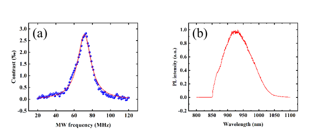
We first characterized the VSi defects ensemble generated by high-dose FIB implantation. The sample was placed in a home-built confocal fluorescence scanning system and excited by a 730 nm laser through an infrared 0.85 N.A. objective (Olympus). To measure the room-temperature (RT) optically detected magnetic resonance (ODMR) spectrum, a 20-m copper wire was paved on the surface of the epitaxy layer to deliver the radio-frequency microwave (MW), which was gated through a switch (ZASWA-2-50DR) and then amplified by a high-power amplifier (ZHL-20W-13+). The fluorescence was collected by a multimode fiber to a Femto (OE-200-Si). There are two nonequivalent silicon defects in 4H-SiC widmann2015coherent , the hexagonal lattice site VSi defects (V1) with good properties in low temperaturenagy2018quantum ; nagy2019high ; morioka2020spin and the cubic lattice site VSi defects (V2). We focused on the V2 defects for they can be manipulated at even room temperature widmann2015coherent ; carter2015spin ; simin2017locking . Fig 1.(a) shows an ODMR contrast of about 0.28 , with a linewidth (full width at half maximum) of MHz, which was similar to previous works wang2017efficient ; wang2019demand ; wang2017scalable . The resonant frequency was MHz, corresponding to the zero-field-splitting for V2 silicon defects at room temperature widmann2015coherent . We further measured the RT photoluminescence (PL) spectrum of V2 silicon defects using a spectrometer (iHR550, Horiba), as shown in Fig 1.(b). The observed spectrum was in the near-infrared range, which was similar to the previous results of the VSi ensemble and single VSi defect measured at room temperature widmann2015coherent ; fuchs2015engineering ; wang2017efficient ; wang2019demand ; wang2017scalable .
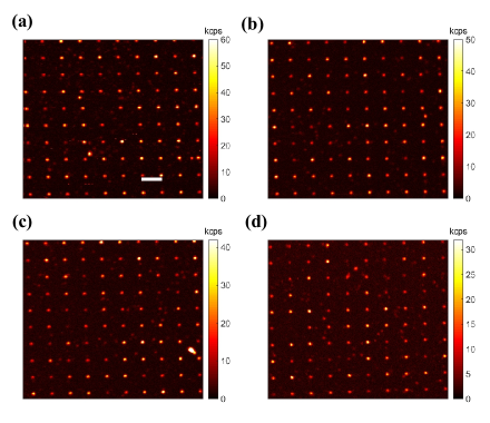
We proceeded to perform the experiment on the VSi defect arrays generated by the FIB with low implantation doses. We optimized the dwell time and beam current of the HIM to change the implantation dose per spot. We found that the dwell time has a linear relation with the dose at a certain current (see table S1 in SI for more details). The fluorescence of VSi defects were collected by a 1.3 N.A. oil objective (Nikon) to enhance the collection efficiency, then separated by a 50:50 beam splitter and coupled to two avalanche photodiodes (APDs) with a 40-m-diameter pinhole. The confocal scanning images under an excitation laser power of 0.5 mW for defect arrays generated at doses ranging from 100 to 40 ions/spot are shown in Fig 2. For each 10 10 array, the spots were separated by 3 m. The fluorescence intensity for each spot decreased significantly with the dose reduction. The corresponding statistics of generated VSi defects per spot at different doses are shown in section S3 in SI. As described below, the generated rate of a single VSi reduced exponentially with the dose. We then further reduced the dose to increase the generation rate of single VSi defects.
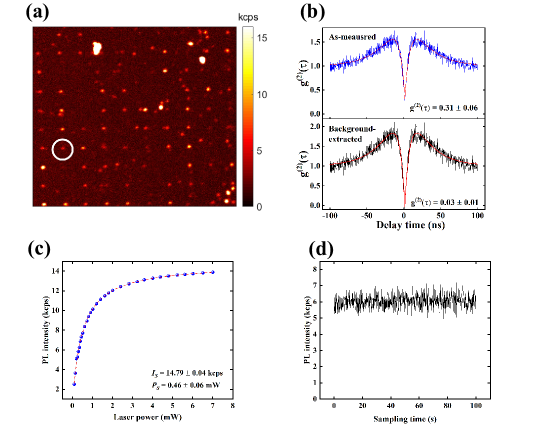
When the FIB dose reduced to 20 ions/spot (the lowest dose that HIM can achieve), the array was still obvious, as shown in Fig 3.(a). However, the fluorescence intensity for a particular spot was comparably weak, which was similar to the reported intensity of a single VSi wang2017efficient ; wang2019demand ; wang2017scalable . To identify single VSi defect centers, we measured the second-order autocorrelation functions () of the generated color centers ( is the time delay between two paths). We present the result of the single VSi defect in the white circle in Fig 3.(a) as an example. When excited by a laser power of 0.5 mW, the signal counts kcps (kilo counts per second) and the background counts kcps. Since the intensity of background was comparable with signal, the as-measured data normalized data () was corrected using , where . As it is shown in Fig 3.(b), we fitted both the as-measured (upper panel) and background-extracted (lower panel) data with , where , , and are fitting parameters. The fitted were and , respectively, both were far below 0.5, verifying that it is a single Vsi defect. We then measured the PL intensity as a function of excitation laser power (Fig 3.(c)). The red line is the fit using , where is the maximum intensity, and is the saturation laser power. Inferred from the fit, mW and kcps, respectively. Since the stability of a single-photon source is also crucial in quantum information applications, we traced the PL intensity of the VSi defect under an excitation laser power of 0.5 mW with a sampling time of 100 s, as shown in Fig 3.(d). The intensity kept stable with no blinking or bleaching, showing that the synthesized single VSi defect has excellent photostability.
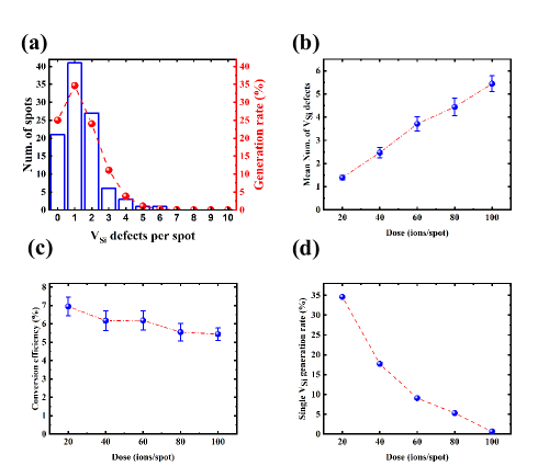
To analyze the effect of implantation dose, we systematically counted and estimated the number of generated VSi defects in each spot at different doses with a sampling size of 100 spots. The statistic method used was similar to the previous worksBabin_2021 ; chen2019laser ; chen2017laser . By combining fluorescence intensity detection and measuring , we found that the number of VSi defects per spot could be estimated by a fluorescence intensity unit of 8 kcps, which was approximately the intensity of one VSi defect under an excitation laser power of 0.5 mW (see section S3 in SI for the methodology to estimate the number of color centers per spot). The mean number of VSi defects and the inferred generation rates were fitted by a Poisson distribution function , where is the mean number of VSi defects per spot. As a representative, the statistics of VSi defects generated at a dose of 20 ions/spot are shown in Fig 4.(a). The blue histograms are the counting results, and the red line is the Poisson fit. At a dose of 100 ions/spot, up to 10 VSi defects can be generated within a spot, with . It was hard to find single VSi defects (the number of single VSi defects within 100 spots is usually smaller than 3) until the FIB dose was reduced to 40 ions/spot, with 17 single VSi defects to be identified in the 10 10 arrays (Fig 2.(a)). In the lowest FIB dose of 20 ions/spot, 41 single VSi defects occurred in the 10 10 array, with . The inferred generation rate for a single VSi defect was 35 . With an average implantation dose of 20 ions/spot, the conversion yield of He+ ions to VSi defects was estimated to be 6.95 , which was similar to the former He+ ions implantation experiment Babin_2021 . Similar analysis can be applied to cases of other doses. The mean number of VSi defects per spot and the conversion yields as a function of dose are visible in Fig 4.(b) and (c), respectively. The conversion yield increased with the reduction of implantation dose, from 5.44 to 6.95 . Such a phenomenon has been observed in the Si2+ FIB experiment in SiC wang2017scalable . Also, the inferred single VSi defect generation rate increased as the dose decreased, as shown in Fig 4.(d). The generation rate of a single VSi defect ( 35 ) was comparable with previous works of mask-assisted helium-ion, carbon-ion implantation and Si2+ FIB experimentBabin_2021 ; wang2017efficient ; wang2019demand ; wang2017scalable . However, a drawback of carbon and silicon ion implantation is that the residual lattice damage is significant, which degrades the spin properties of spin defects. Such a phenomenon has been observed in nitrogen-ion-implanted NV centers in the diamond favaro2017tailoring . Compared with carbon and silicon ions, helium has a smaller atomic mass, which causes smaller damage and a deeper implantation depth when accelerated by the same kinetic energy. The charge state of induced spin defects is inferred to be more stable due to the gentle damage caused by helium ions. Furthermore, the effects of surface noise will degrade with a deeper implantation depth and prospect and longer spin coherent time, inferred from the case of NV centers in the diamondPhysRevLett.113.027602 ; favaro2017tailoring ; PhysRevX.9.031052 .
Conclusion
In conclusion, we investigated a maskless and targeted method for precisely generating single VSi defects arrays in 4H-SiC using a high-resolution helium-ion microscope. ODMR and PL spectra measurements confirmed the types of generated defects. The fluorescence properties of single VSi defects were characterized, showing excellent single-photon properties, photostability, and saturation intensity of 15 kcps. The effects of FIB dose were systematically studied, and the conversion yield and generation rate of single VSi defects rise with the reduction of the dose. A conversion yield of 6.95 and a generation rate of 35 for a single VSi defect were realized at a dose of 20 ions/spot. Due to the high generation rate of the single defect and the precise control of implantation position, this work is meaningful for the applications in integrating color centers to semiconductor-based microstructures like waveguides, nanopillars, and photonic crystal cavities Babin_2021 ; radulaski2017scalable ; bracher2017selective , precise quantum sensing based on optically-addressable spin defects kraus2014magnetic ; simin2015high ; niethammer2016vector , and thus benefits the quantum information process on spin-to-photon interface morioka2020spin ; Babin_2021 ; soykal2016silicon .
Supplementary Information
S1. The helium-ion microscope
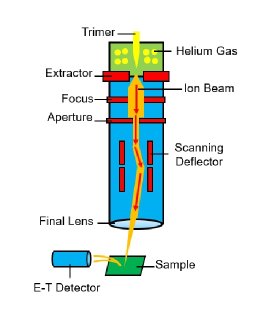
The helium-ion microscope (HIM) components are shown in Fig 5. There is a single crystal tungsten trimer composed of three tungsten atoms in gas helium with a low pressure of 10-6 Torr. Helium atoms are ionized into three beam currents by the high voltage of the trimer. One of the beam currents will be selected and extracted by the extractor and focused on the ion beam. After passing an aperture of 20 m, it will be deflected and focused into a spot with a sub-0.5 nm diameter, scanning the target surface. The E-T detector captures the secondary electrons excited by the incident ions spot by spot to realize a 0.5 nm resolution image, which is helpful for the on-demand FIB implantation and the integration of color centers to nanostructure.
There are two kinds of implantation modes of HIM. The first one is the spot mode. The helium ion beam is focused within a diameter smaller than 0.5 nm in this mode. The implantation doses are controlled by the beam current and dwell time on each spot. The second mode is roaster scanning mode. Implantation can be realized within a specific geometry after setting the number of ions in the unit area (ions/cm2), slightly different from spot mode with a dose unit of ions/spot. We use scanning mode to generate VSi defects ensemble strip and spot mode to generate VSi defects arrays.
It is noticed that the perturbation of beam current from the set value (0.4 pA) is within the tolerance when HIM is working. As shown in TABLE S1, the dwell time has a linear relation with the dose with a particular beam current. The accuracy of incident ions is determined by the accuracy of HIM’s dwell time, which is about 0.1 s. With a beam current of about 0.4 pA, a dwell time of 0.1 s determines a dose deviation of about 0.25 ions/spot.
| Dose (ions/spot) | Dwell time (s) | Beam current (pA) |
|---|---|---|
| 100 | 37.6 | 0.420 |
| 80 | 31.2 | 0.419 |
| 60 | 23.8 | 0.423 |
| 40 | 15.6 | 0.417 |
| 20 | 7.9 | 0.412 |
S2. SRIM simulation of the depth distribution of He+-ions-generated silicon vacancies
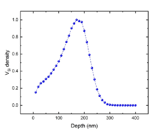
We use the stopping and range of ions in matter (SRIM) simulation to simulate the process of 30 keV He+ ions implantation. As shown in Fig 6, the simulated implantation depth is about 179 nm, with a longitudinal straggling of 47.4 nm.

S3. The analysis of VSi defects generation rate
| Luminescence intensity under 0.5 mW (kcps) | Number of VSi defects | |
|---|---|---|
| 4 8 | 0 0.32 | 1 |
| 8 16 | 0.32 0.65 | 2 |
We estimate the number of VSi centers by combining the HBT experiment and measuring the luminescence intensity. We measured the second-order autocorrelation functions of picked color centers within a 10 10 array under a laser power of 0.5 mW, which were clarified into different groups by luminescence intensity levels. And every group contains at least four color centers. We found that the luminescence intensity and satisfied the relation in the table below.
According to the previous work, color centers with a from 0 to 0.32 are identified as single-photon sources, and color centers with from 0.33 to 0.65 are clarified as double-photon sources. We measured several spots with intensity from 4 to 8 kcps and from 8 to 16 kcps, respectively, all the measured color centers satisfied the relationship in Table S2. In Fig 7, we showed the second-order autocorrelation function of a spot with a luminescence intensity of 13.5 kcps as a typical double-photon source, with . Hence, we can assume that an intensity unit of 8 kcps corresponds to one silicon vacancy. Since the luminescence intensity of a single silicon vacancy is low, it will be time-consuming to measure of all the spots, especially those containing 3 silicon vacancies or more, whose number of color centers can be estimated by the assumed intensity unit. For example, a spot with a luminescence intensity of 23 kcps contains 3 VSi defects and a spot with a luminescence intensity of 46 kcps contains 6 VSi defects.
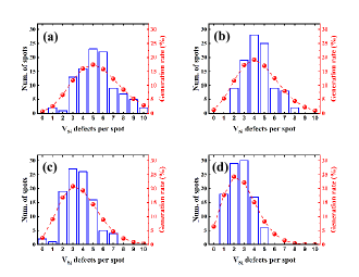
At each dose, we statistic the number of spots with a corresponding number of generated VSi defects per spot in a 10 10 array, shown in blue histograms in Fig 8. By normalizing the number and using the Poisson fitting function mentioned in the main text, we can infer the possibility to generate () VSi defects per spot, which is equal to the generation rate (Red lines and dots in Fig 8). The statistics of generated VSi defects from 100 He+ ions/spot to He+ 40 ions/spot are shown in Fig 8, and the statistics of generated VSi defects at 20 He+ ions/spot are shown in Fig 4.(a) in the main text.
Conflicts of Interest
There are no conflicts to declare.
Acknowledgments
The FIB experiment was carried out at the Center for Micro and Nanoscale Research and Fabrication at University of Science and Technology of China. This work was supported by the Innovation Program for Quantum Science and Technology (Grants No. 2021ZD0301400), the National Natural Science Foundation of China (Grants No. 61725504, No. 11774335, No. 11821404, and No. U19A2075), the Anhui Initiative in Quantum Information Technologies (Grants No. AHY020100, and No. AHY060300), the Fundamental Research Funds for the Central Universities (Grant No. WK2030380017), and the China Postdoctoral Science Foundation (Grants No. BX20200326 and 2021M693099).
References
- (1) Koehl, William F and Buckley, Bob B and Heremans, F Joseph and Calusine, Greg and Awschalom, David D, Room temperature coherent control of defect spin qubits in silicon carbide, Nature, 2011, 479, 84-87.
- (2) Falk, Abram L and Buckley, Bob B and Calusine, Greg and Koehl, William F and Dobrovitski, Viatcheslav V and Politi, Alberto and Zorman, Christian A and Feng, Philip X-L and Awschalom, David D, Polytype control of spin qubits in silicon carbide, Nat. Commun., 2013, 4, 1-7.
- (3) Christle, David J and Falk, Abram L and Andrich, Paolo and Klimov, Paul V and Hassan, Jawad Ul and Son, Nguyen T and Janzén, Erik and Ohshima, Takeshi and Awschalom, David D, Isolated electron spins in silicon carbide with millisecond coherence times, Nat. Mater., 2015, 14, 160-163.
- (4) Widmann, Matthias and Lee, Sang-Yun and Rendler, Torsten and Son, Nguyen Tien and Fedder, Helmut and Paik, Seoyoung and Yang, Li-Ping and Zhao, Nan and Yang, Sen and Booker, Ian, Coherent control of single spins in silicon carbide at room temperature, Nat. Mater., 2015, 14, 164-168.
- (5) Nagy, Roland and Widmann, Matthias and Niethammer, Matthias and Dasari, Durga BR and Gerhardt, Ilja and Soykal, Öney O and Radulaski, Marina and Ohshima, Takeshi and Vučković, Jelena and Son, Nguyen Tien and others, Quantum properties of dichroic silicon vacancies in silicon carbide Phys. Rev. Appl., 2018, 9, 034022.
- (6) Fuchs, F and Stender, B and Trupke, M and Simin, D and Pflaum, J and Dyakonov, V and Astakhov, GV, Engineering near-infrared single-photon emitters with optically active spins in ultrapure silicon carbide Nat. Commun., 2015, 6, 1-7.
- (7) Nagy, Roland and Niethammer, Matthias and Widmann, Matthias and Chen, Yu-Chen and Udvarhelyi, Péter and Bonato, Cristian and Hassan, Jawad Ul and Karhu, Robin and Ivanov, Ivan G and Son, Nguyen Tien, High-fidelity spin and optical control of single silicon-vacancy centres in silicon carbide, Nat. Commun., 2019, textbf10, 1-8.
- (8) Yang, Li-Ping and Burk, Christian and Widmann, Matthias and Lee, Sang-Yun and Wrachtrup, Jörg and Zhao, Nan, Electron spin decoherence in silicon carbide nuclear spin bath Phys. Rev. B, 2014, 90, 241203.
- (9) Carter, SG and Soykal, ÖO and Dev, Pratibha and Economou, Sophia E and Glaser, ER, Spin coherence and echo modulation of the silicon vacancy in 4 H- SiC at room temperature Phys. Rev. B, 2015, 92, 161202.
- (10) Son, Nguyen T and Anderson, Christopher P and Bourassa, Alexandre and Miao, Kevin C and Babin, Charles and Widmann, Matthias and Niethammer, Matthias and Ul Hassan, Jawad and Morioka, Naoya and Ivanov, Ivan G, Developing silicon carbide for quantum spintronics, Appl. Phys. Lett., 2020, 116, 190501.
- (11) Christle, David J and Klimov, Paul V and Charles, F and Szász, Krisztián and Ivády, Viktor and Jokubavicius, Valdas and Hassan, Jawad Ul and Syväjärvi, Mikael and Koehl, William F and Ohshima, Takeshi, Isolated spin qubits in SiC with a high-fidelity infrared spin-to-photon interface, Phys. Rev. X, 2017, 7, 021046.
- (12) Morioka, Naoya and Babin, Charles and Nagy, Roland and Gediz, Izel and Hesselmeier, Erik and Liu, Di and Joliffe, Matthew and Niethammer, Matthias and Dasari, Durga and Vorobyov, Vadim and others, Spin-controlled generation of indistinguishable and distinguishable photons from silicon vacancy centres in silicon carbide, Nat. Commun., 2020, 11, 1-8.
- (13) Charles Babin and Rainer Stöhr and Naoya Morioka and Tobias Linkewitz and Timo Steidl and Raphael Wörnle and Di Liu and Erik Hesselmeier and Vadim Vorobyov and Andrej Denisenko and Mario Hentschel and Christian Gobert and Patrick Berwian and Georgy V. Astakhov and Wolfgang Knolle and Sridhar Majety and Pranta Saha and Marina Radulaski and Nguyen Tien Son and Jawad Ul-Hassan and Florian Kaiser and Jörg Wrachtrup, Fabrication and nanophotonic waveguide integration of silicon carbide colour centres with preserved spin-optical coherence, Nat. Mater., 2021, 21, 67-73.
- (14) Soykal, ÖO and Dev, Pratibha and Economou, Sophia E, Silicon vacancy center in 4 H-SiC: Electronic structure and spin-photon interfaces Phys. Rev. B, 2016, 93, 081207.
- (15) Wang, Jun-Feng and Yan, Fei-Fei and Li, Qiang and Liu, Zheng-Hao and Liu, He and Guo, Guo-Ping and Guo, Li-Ping and Zhou, Xiong and Cui, Jin-Ming and Wang, Jian, Coherent control of nitrogen-vacancy center spins in silicon carbide at room temperature, Phys. Rev. Lett., 2020, 124, 223601.
- (16) Mu, Zhao and Zargaleh, Soroush Abbasi and von Bardeleben, Hans Jurgen and Froöch, Johannes E and Nonahal, Milad and Cai, Hongbing and Yang, Xinge and Yang, Jianqun and Li, Xingji and Aharonovich, Igor and others, Coherent manipulation with resonant excitation and single emitter creation of nitrogen vacancy centers in 4H silicon carbide, Nano Lett., 2020, 20, 6142-6147.
- (17) Simin, D and Kraus, H and Sperlich, A and Ohshima, T and Astakhov, GV and Dyakonov, V, Locking of electron spin coherence above 20 ms in natural silicon carbide, Phys. Rev. B, 2017, 95, 161201.
- (18) Kraus, H and Soltamov, VA and Fuchs, F and Simin, D and Sperlich, A and Baranov, PG and Astakhov, GV and Dyakonov, Vladimir, Magnetic field and temperature sensing with atomic-scale spin defects in silicon carbide, Sci. Rep., 2014, 4, 1-8.
- (19) Simin, D and Fuchs, F and Kraus, H and Sperlich, A and Baranov, PG and Astakhov, GV and Dyakonov, V, High-precision angle-resolved magnetometry with uniaxial quantum centers in silicon carbide, Phys. Rev. Appl., 2015, 4, 014009.
- (20) Niethammer, Matthias and Widmann, Matthias and Lee, Sang-Yun and Stenberg, Pontus and Kordina, Olof and Ohshima, Takeshi and Son, Nguyen Tien and Janzén, Erik and Wrachtrup, Jörg, Vector Magnetometry Using Silicon Vacancies in 4 H-SiC Under Ambient Conditions Phys. Rev. Appl., 2016, 6, 034001.
- (21) Banks, Hunter B and Soykal, Öney O and Myers-Ward, Rachael L and Gaskill, D Kurt and Reinecke, TL and Carter, Samuel G, Resonant Optical Spin Initialization and Readout of Single Silicon Vacancies in 4 H-Si C Phys. Rev. Appl., 2019, 11, 024013.
- (22) Radulaski, Marina and Widmann, Matthias and Niethammer, Matthias and Zhang, Jingyuan Linda and Lee, Sang-Yun and Rendler, Torsten and Lagoudakis, Konstantinos G and Son, Nguyen Tien and Janzen, Erik and Ohshima, Takeshi, Scalable quantum photonics with single color centers in silicon carbide, Nano Lett., 2017, 17, 1782-1786.
- (23) Bracher, David O and Zhang, Xingyu and Hu, Evelyn L, Selective Purcell enhancement of two closely linked zero-phonon transitions of a silicon carbide color center, Proc. Natl. Acad. Sci. U.S.A., 2017, 114, 4060-4065.
- (24) Wang, Junfeng and Zhou, Yu and Zhang, Xiaoming and Liu, Fucai and Li, Yan and Li, Ke and Liu, Zheng and Wang, Guanzhong and Gao, Weibo, Efficient generation of an array of single silicon-vacancy defects in silicon carbide, Phys. Rev. Appl., 2017, 7, 064021.
- (25) Wang, Jun-Feng and Li, Qiang and Yan, Fei-Fei and Liu, He and Guo, Guo-Ping and Zhang, Wei-Ping and Zhou, Xiong and Guo, Li-Ping and Lin, Zhi-Hai and Cui, Jin-Ming, On-demand generation of single silicon vacancy defects in silicon carbide, ACS Photon., 2019, 6, 1736-1743.
- (26) Chen, Yu-Chen and Salter, Patrick S and Niethammer, Matthias and Widmann, Matthias and Kaiser, Florian and Nagy, Roland and Morioka, Naoya and Babin, Charles and Erlekampf, Jüurgen and Berwian, Patrick, Laser writing of scalable single color centers in silicon carbide, Nano Lett., 2019, 19, 2377-2383.
- (27) Kraus, H and Simin, D and Kasper, C and Suda, Y and Kawabata, S and Kada, W and Honda, T and Hijikata, Y and Ohshima, T and Dyakonov, V, Three-dimensional proton beam writing of optically active coherent vacancy spins in silicon carbide Nano Lett., 2017, 17, 2865-2870.
- (28) Ohshima, Takeshi and Satoh, Takahiro and Kraus, Hannes and Astakhov, Georgy V and Dyakonov, Vladimir and Baranov, Pavel G, Creation of silicon vacancy in silicon carbide by proton beam writing toward quantum sensing applications, J. Phys. D: Appl. Phys., 2018, 51, 333002.
- (29) Wang, Junfeng and Zhang, Xiaoming and Zhou, Yu and Li, Ke and Wang, Ziyu and Peddibhotla, Phani and Liu, Fucai and Bauerdick, Sven and Rudzinski, Axel and Liu, Zheng, Scalable fabrication of single silicon vacancy defect arrays in silicon carbide using focused ion beam, Acs Photon., 2017, 4, 1054-1059.
- (30) Pavunny, Shojan P and Yeats, Andrew L and Banks, Hunter B and Bielejec, Edward and Myers-Ward, Rachael L and DeJarld, Matthew T and Bracker, Allan S and Gaskill, D Kurt and Carter, Samuel G, Arrays of Si vacancies in 4H-SiC produced by focused Li ion beam implantation, Sci. Rep., 2021, 11, 1-8.
- (31) Hollenbach, M and Klingner, N and Jagtap, NS and Bischoff, L and Fowley, C and Kentsch, U and Hlawacek, G and Erbe, A and Abrosimov, NV and Helm, M and others, Wafer-scale nanofabrication of telecom single-photon emitters in silicon, arXiv, 2022, 4, 13173.
- (32) Huang, Z and Li, W-D and Santori, C and Acosta, VM and Faraon, A and Ishikawa, T and Wu, W and Winston, D and Williams, RS and Beausoleil, RG, Diamond nitrogen-vacancy centers created by scanning focused helium ion beam and annealing, Appl. Phys. Lett., 2013, 8, 081906.
- (33) McCloskey, D and Fox, D and O’Hara, N and Usov, V and Scanlan, D and McEvoy, N and Duesberg, GS and Cross, GLW and Zhang, HZ and Donegan, JF, Helium ion microscope generated nitrogen-vacancy centres in type Ib diamond, Appl. Phys. Lett., 2014, 104, 031109.
- (34) Myers, B. A. and Das, A. and Dartiailh, M. C. and Ohno, K. and Awschalom, D. D. and Bleszynski Jayich, A. C., Probing Surface Noise with Depth-Calibrated Spins in Diamond, Phys. Rev. Lett., 2014, 113, 027602.
- (35) Fávaro de Oliveira, Felipe and Antonov, Denis and Wang, Ya and Neumann, Philipp and Momenzadeh, Seyed Ali and Häußermann, Timo and Pasquarelli, Alberto and Denisenko, Andrej and Wrachtrup, Jörg, Tailoring spin defects in diamond by lattice charging, Nat. Commun., 2017, 8, 1-8.
- (36) Sangtawesin, Sorawis and Dwyer, Bo L. and Srinivasan, Srikanth and Allred, James J. and Rodgers, Lila V. H. and De Greve, Kristiaan and Stacey, Alastair and Dontschuk, Nikolai and O’Donnell, Kane M. and Hu, Di and Evans, D. Andrew and Jaye, Cherno and Fischer, Daniel A. and Markham, Matthew L. and Twitchen, Daniel J. and Park, Hongkun and Lukin, Mikhail D. and de Leon, Nathalie P., Origins of Diamond Surface Noise Probed by Correlating Single-Spin Measurements with Surface Spectroscopy Phys. Rev. X, 2019, 9, 031052.
- (37) Chen, Yu-Chen and Salter, Patrick S and Knauer, Sebastian and Weng, Laiyi and Frangeskou, Angelo C and Stephen, Colin J and Ishmael, Shazeaa N and Dolan, Philip R and Johnson, Sam and Green, Ben L, Laser writing of coherent colour centres in diamond, Nat. Photon., 2017, 11, 77-80.