Field effect two-dimensional electron gases in modulation-doped InSb surface quantum wells
Abstract
We report on transport characteristics of field effect two-dimensional electron gases (2DEG) in surface indium antimonide quantum wells. The topmost 5 nm of the 30 nm wide quantum well is doped and shown to promote the formation of reliable, low resistance Ohmic contacts to surface InSb 2DEGs. High quality single-subband magnetotransport with clear quantized integer quantum Hall plateaus are observed to filling factor in magnetic fields of up to T. We show that the electron density is gate-tunable, reproducible, and stable from pinch-off to 4 cm-2, and peak mobilities exceed 24,000 cm2/Vs. Large Rashba spin-orbit coefficients up to 110 meVÅ are obtained through weak anti-localization measurements. An effective mass of 0.019 is determined from temperature-dependent magnetoresistance measurements, and a g-factor of 41 at a density of 3.6 cm-2 is obtained from coincidence measurements in tilted magnetic fields. By comparing two heterostructures with and without a delta-doped layer beneath the quantum well, we find that the carrier density is stable with time when doping in the ternary Al0.1In0.9Sb barrier is not present. Finally, the effect of modulation doping on structural asymmetry between the two heterostructures is characterized.
Confining potentials in electrostatically-defined nanoscale devices, such as single electron transistors or single electron pumps, are strongly enhanced in two-dimensional electron gases (2DEGs) hosted at the surface or near the surface of semiconductor heterostructures.[1] Furthermore, surface or near-surface quantum well (QW) heterostructures in III-V semiconductors are compatible with proximitized superconductivity and offer a scalable planar platform for superconductor-semiconductor systems, such as those suggested for topological quantum computation[2, 3] and those suitable for topological phase transitions involving Majorana zero modes.[4, 5, 6] Amongst III-V binary semiconductors, Indium Antimonide (InSb) has the smallest electron effective mass, highest spin orbit coupling [7, 8], and largest Landé g-factor. Such material properties makes the pursuit of InSb QWs desirable for a number of quantum device applications, including quantum sensing, quantum metrology, and quantum computing.
High quality two-dimensional electron gases (2DEGs) in InSb QWs are difficult to realize partly due to the highly mismatched lattice constants between the quantum well and barrier materials,[9] the available purity of the required base elements (In, Sb),[10] and the lack of wafer-to-wafer reproducibility with doping schemes.[11] InSb QWs have generally relied on the use of modulation-doping for 2DEG formation, but these structures have frequently reported issues with parasitic parallel conduction and unstable carrier densities.[12, 13, 14, 15] This is especially true of InSb surface QWs, which must contend with a Schottky barrier at the surface. Dopant-free field-effect 2DEGs avoid these issues and have recently been reported in undoped InSb QWs.[16] However, as reported in GaAs systems, achieving good Ohmic contacts is challenging in completely undoped heterostructures, especially near the surface.[17]
In this Letter, we report on the use of a thin -InSb layer to promote the formation of reliable, low resistance Ohmic contacts to a surface InSb QW. We compare two InSb surface QW heterostructures, one with and one without a delta-doped Al0.1In0.9Sb layer, and demonstrate the influence of modulation doping on gating characteristics, magnetotransport behavior, and spin-orbit interaction. We overcome issues of parallel conduction in both heterostructures and present magnetotransport behavior of a high quality, single-subband 2DEG up to 18 T. The effective mass, transport and quantum lifetimes, and g-factor are determined from magnetoresistance measurements. The strength of Rashba spin-orbit interaction is characterized using weak anti-localization measurements.
Two wafers, G1 and G2, were grown by molecular beam epitaxy (MBE). Wafer G1 had the following sequence of layers (see Figure 1), starting from a 3” semi-insulating (SI) GaAs (001) substrate: a 120 nm GaAs smoothing layer, 100 nm AlSb nucleation layer, a 4 µm Al0.1In0.9Sb dislocation filter buffer, a 30 nm InSb quantum well where the topmost 5 nm was doped with Si at a doping density of cm-3. Wafer G2 is identical to wafer G1, except for an additional Si delta-doped layer (with sheet doping density cm-2) located 10 nm below the InSb quantum well. Section I in the Supplementary Material provides additional details about MBE growth. In both wafers, the doped -InSb layer facilitates the low-temperature formation of low-resistance Ohmic contacts to the 2DEG. The purpose of the delta-doped layer below the InSb quantum well in G2 is to pull the 2DEG wavefunction further away from the surface than in G1. Section II from the Supplementary Material shows self-consistent simulations[18, 19, 20] of the bandstructure profiles for both G1 and G2.
| Wafer G1 | Wafer G2 | ||
|---|---|---|---|
| Hall bar | peak mobility | Hall bar | peak mobility |
| ID | (cm2/Vs) | ID | (cm2/Vs) |
| G1-1 | 18,000 | G2-1 | 21,800 |
| G1-2 | 22,200 | G2-2 | 24,400 |
| G1-3 | 21,200 | G2-3 | 24,600 |
| G1-4 | 23,100 | G2-4 | 24,100 |
Eight gated Hall bars (see Table 1 and Figure 1) were fabricated using standard optical lithography and wet-etching techniques, keeping all processes at or below a temperature of 150∘C to prevent the deterioration of device characteristics,[21, 22, 14] and preventing the InSb surface from coming into contact with photoresist developer (see Section III of the Supplementary Material for more details on sample fabrication). Ti/Au Ohmic contacts were deposited directly on the doped -InSb layer. Immediately prior to deposition, Ohmic contacts were treated with a sulfur passivation solution. The latter is designed to etch away native oxides, prevent further surface oxidation during transfer in air to the deposition chamber, and possibly dope the surface.[23, 24, 25] Combined with the presence of Si dopants at the surface of the InSb quantum well, Ohmic contacts with typical resistances of 400800 were achieved in zero magnetic field, and 12 k at T. Finally, 60 nm thick hafnium dioxide (HfO2) was deposited by atomic layer deposition (ALD) at 150∘C, followed by the deposition of a Ti/Au global top-gate that overlaps the Ohmic contacts.
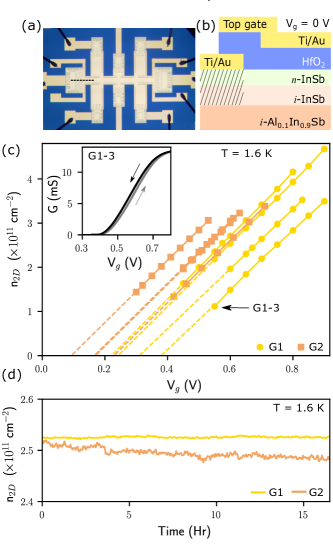
Using standard ac lock-in measurement techniques (see Section IV of the Supplementary Material for circuit diagrams and experimental details), four-terminal and two-terminal transport experiments were performed in a pumped-4He cryostat and a 3He/4He dilution refrigerator, with a base temperature of 1.6 K and 11 mK respectively. In ungated Hall bars, the as-grown electron densities of G1 and G2 were cm-2 and cm-2, respectively. However, in all gated Hall bars, the quantum well in both wafers is completely depleted of electrons at top-gate voltage V, most likely due to significant trapped charges associated with HfO2.[22, 26] A positive top-gate voltage is needed for a 2DEG to form. The 2DEG turn-on threshold voltage is the intercept of the electron density n2D(Vg) on the top-gate voltage axis in Figure 1(c), obtained from the linear extrapolation of the data for each Hall bar to n.111This definition removes any ambiguity in the turn-on threshold due to the transition from the Boltzmann transport regime to the percolation regime at low electron densities. The average 2DEG turn-on threshold is V V for wafer G1 and V V for wafer G2. The lower threshold in wafer G2 is consistent with the additional doping provided by its delta-doped layer, which brings the conduction band closer to the Fermi level in wafer G2 than in wafer G1. Magnetotransport plots at K for six samples are shown in Section IV of the Supplementary Material.
The inset of Figure 1(c) shows a typical pinch-off curve for a gated Hall bar from wafer G1 in a two-terminal conductance measurement. Agreement between the pinch-off voltage ( V) from the two-terminal measurement and the extrapolated 2DEG turn-on threshold ( V) from the four-terminal measurement, both obtained from the same Hall bar, strongly indicates that there is no significant tunnel barrier within the Ohmic contacts themselves.[28] Indeed, the electron density in the InSb quantum well directly underneath the Ohmic contact metal should be the same as or very similar to the as-grown electron density, because the HfO2 dielectric is not in direct contact with -InSb (i.e., there is not a large trapped charge density). The pinch-off curves are stable and reproducible, overlapping perfectly when is swept in the same direction and showing minimal hysteresis when is swept in opposite directions. After pinch-off, the 2DEG does not turn itself back on with time.[16, 13, 15] To further illustrate this time stability, Figure 1(d) shows the carrier density measured over a period of 16 hours, where it essentially stays constant. This is not however the case with devices from G2, where the electron density can drift with time. We speculate this could be due to the presence of dopants in the Al0.1In0.9Sb layer. Indeed, quantum dots fabricated in InSb 2DEGs with modulation-doped AlInSb have recently been reported where their characteristics drift in time.[14]
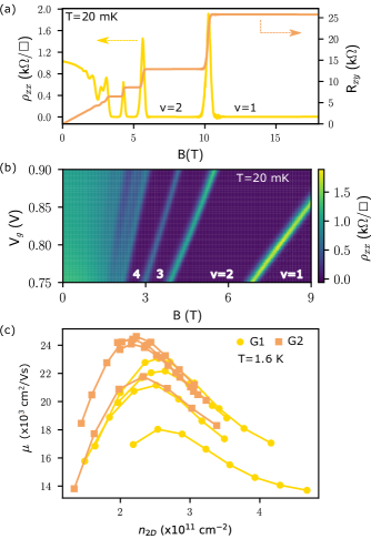
Figure 2(a) shows the transverse (Hall) resistance and longitudinal resistivity in a magnetic field up to T at the highest accessible carrier density cm-2 for sample G1-3. The transverse resistance exhibits well-defined quantized quantum Hall plateaus at filling factors and 4, where is the Planck constant and is the single electron charge. The population of a single subband is evidenced by the observation of single-frequency Shubnikov-de-Haas oscillations in combination with vanishing at . Furthermore, the 2DEG density determined from the periodicity of Shubnikov-de-Haas oscillations versus inverse field, given by , matches the total carrier density determined via the classical Hall effect . No signs of parallel conduction from either a second subband or another conductive layer is discernible. The absence of Landau level crossings in the Landau fan diagram shown in Figure 2(b) indicates the single subband behavior persists over the entire measured density range. The Landau fan, obtained by sweeping the top-gate at magnetic field increments on sample G1-3, showcases the reproducibility and stability of gating characteristics.
The dependence of the transport mobility on 2DEG density is shown in Figure 2(c) which shows an average peak mobility of cm2/Vs near cm-2 in G1. The decrease in mobility at higher densities is attributed to increasing interface roughness scattering[29, 30] as the electron wavefunction is pulled closer to the surface by the increasing electric field of the top-gate. Increased scattering from a populating second subband is ruled out, since there is only one subband populated over that range of density. Alloy scattering (typically only observed in ternary alloys) is also ruled out, since the 2DEG wavefunction lies almost entirely within the InSb quantum well. The higher average peak mobility of cm2/Vs near cm-2 in G2 is consistent with its 2DEG being pulled further away from the surface by the delta-doped layer, relative to G1. The greater device-to-device reproducibility in G2 than in G1 is also consistent with this picture. Variability between nominally identical devices may be mostly due to surface treatment during sample fabrication. The mobilities reported here could perhaps be improved further[9] by reducing the density of threading dislocations[31, 32] and hillocks.[33, 34]
Figure 3(a) shows the temperature dependence of the amplitude of low-field SdH oscillations in sample G2-4, obtained by subtracting a polynomial background from . The data was taken at a density of cm-2, determined from the periodicity of SdH oscillations versus inverse magnetic field shown in the inset. The temperature-dependent amplitude A of the minimum at T, normalized by the base temperature value ASdH ( K), is plotted in Figure 3(b), and fit to theory (see Section V of the Supplementary Material for more details). A value of is obtained, which is higher than 0.014 found in bulk InSb. This larger value for the QW is found to agree quite well with the predictions of an 8-band calculation for a symmetric InSb/In0.9Al0.1Sb QW, as presented in Section VI of the Supplementary Material. Although our QW is not symmetrical, the contribution due to wave function penetration of the barrier layers is shown to be quite small. The most dominant contributions to the mass increase appear to come from enlargement of the QW band gap due to confinement and strain, and from the strong non-parabolicity of the electron dispersion. It should be noted that our experimental fit gives an average parabolic mass that matches the number of states in the filled Landau levels to the number of states in the real non-parabolic dispersion.
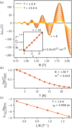
Using the K trace in Figure 3(a), a quantum lifetime ps, also known as the single-particle relaxation time, is extracted from the Dingle plot shown in Figure 3(c) (see Section V of the Supplementary Material for more details). In comparison, the mean transport lifetime derived from the Drude model is 0.21 ps. The ratio of transport to quantum lifetimes is thus . Since is weighted by the scattering angle whereas is related to total scattering, the ratio provides insight into the nature of scattering affecting transport.[35] For transport mobilities limited by large angle scattering (as is the case here due to interface roughness), the ratio approaches unity. In other binary QW heterostructures, large ratios of 40 have been reported in samples where small angle scattering from long range potentials (e.g., remote ionized impurities) was the dominant scattering mechanism, leading to high mobilities and long transport lifetimes [5]. Although our transport lifetime differs by more than a factor of ten from these reports, the quantum lifetimes are comparable and justify our use of dopants in the QW.
The Landé g-factor was measured in sample G1-3 at for two different carrier densities, using a tilted magnetic field approach[36] to identify coincidences between the Zeeman and cyclotron energies , where is the Bohr magneton, is the total magnetic field, and is the component of that is perpendicular to the 2DEG plane. By modeling the evolution of spin-split Landau energy levels, the effective g-factors at cm-2 and at cm-2 were obtained, in agreement with other reports of the effective g-factor in InSb.[37, 16, 38, 39, 40] Section VII in the Supplementary Material contains more experimental and theoretical details of the coincidence experiments.
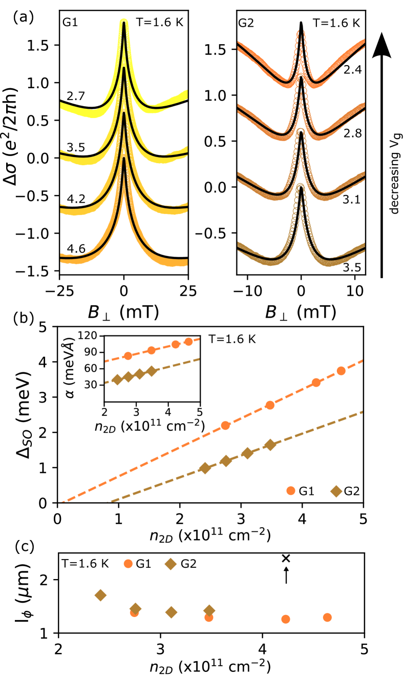
Wafers G1 and G2 are characterized by a strong and tunable spin orbit interaction (SOI), as demonstrated by the weak anti-localization (WAL) conductivity peak observed in all Hall bars. The strength of SOI was determined from fits to using the Hikami-Larkin-Nagaoka (HLN) model,[41] where , is the field-dependent conductivity, and is a constant background conductivity. Figure 4(b) shows the density dependence of the spin-orbit strength in samples G1-1 and G2-1, obtained from fits presented in Figure 4(a). The Rashba coefficient is related to spin orbit length via and where is the energy gap, is the Fermi wave vector, is the diffusion time, and is the spin orbit time. The Rashba coefficient reaches a maximum of nearly 110 meV at cm-2 in G1, among the highest values reported in the literature for InSb[42, 7, 43, 16, 44, 40] (see Table S2 from Section VIII in the Supplementary Material for an explicit comparison), but not as high as in InSbAs.[40, 45] Being related to structural asymmetry, is enhanced by the asymmetry of the wavefunction in the QW at high electric fields. Three factors significantly enhance structural asymmetry in G1: (i) the n-InSb layer inside the QW, (ii) the high- dielectric HfO2 (with ), and (iii) the 2DEG location at the surface. Comparing wafers G1 and G2 in Figure 4(b), is weakened in G2 by nearly a factor of two for all devices measured. The delta-doped Al0.1In0.9Sb layer in G2 is responsible for this behavior: it causes band bending that pulls the 2DEG wavefunction towards the center of the QW, thereby reducing the structural asymmetry and Rashba component of the SOI (see section II in the Supplementary Material for bandstructure profiles of G1 and G2). There is thus a trade-off between mobility and strength of Rashba interactions. Figure 4(c) shows the phase coherence lengths determined from the fits to the HLN model are slightly larger in G2 than those in G1 at K. Within the same wafer, reaches a maximum at the same density as the peak mobility. The phase coherence in G1 increases to 2.4 µm at 22 mK from 1.5 µm at 1.6 K in the same device at a similar carrier density (see Section VIII of the Supplementary Material). In contrast, remains constant from 22 mK to 1.6 K.
In conclusion, we presented the growth, fabrication, and transport characteristics of high-quality, gate-tunable InSb 2DEGs in surface quantum wells grown on (001) SI-GaAs substrates. An -InSb layer within the quantum well was used to realize reliable, low-resistance Ohmic contacts. Magnetoresistance measurements confirmed that intentional dopants in InSb are compatible with high-quality and reproducible transport characteristics, without parasitic parallel conduction or unstable carrier densities. The observation of Rashba coefficients among the highest values reported in the literature for InSb validates the approach of using surface quantum wells. Preliminary evidence suggests intentional dopants in AlxIn1-xSb might be responsible for the drift with time of transport characteristics. If correct, future modulation-doped InSb 2DEG heterostructure with time-wise stable transport characteristics could be achieved by using an InSb/AlxIn1-xSb short-period superlattice (SPSL) doping scheme,[46] where only the very thin (610 monolayers) InSb layers are doped.
Supplementary Material
The eight sections in the Supplementary Material contain additional information on MBE growth, bandstructure profiles, sample fabrication, magnetotransport characterization of Hall bars, effective mass and quantum lifetime measurements, calculations, coincidence experiments and modeling, and weak anti-localization experiments.
E.A.B. and F.S. contributed equally to this paper. The authors thank Christine Nicoll for useful discussions. E.A.B. acknowledges support from a Mike and Ophelia Lazaridis Fellowship. This research was undertaken thanks in part to funding from the Canada First Research Excellence Fund (Transformative Quantum Technologies) and the Natural Sciences and Engineering Research Council (NSERC) of Canada. The University of Waterloo’s QNFCF facility was used for this work. This infrastructure would not be possible without the significant contributions of CFREF-TQT, CFI, ISED, the Ontario Ministry of Research and Innovation, and Mike and Ophelia Lazaridis. Their support is gratefully acknowledged.
References
- Buonacorsi et al. [2021] B. Buonacorsi, F. Sfigakis, A. Shetty, M. Tam, H. Kim, S. Harrigan, F. Hohls, M. Reimer, Z. Wasilewski, and J. Baugh, “Non-adiabatic single-electron pumps in a dopant-free GaAs/AlGaAs 2DEG,” Applied Physics Letters 119, 114001 (2021).
- Shabani et al. [2016] J. Shabani, M. Kjærgaard, H. J. Suominen, Y. Kim, F. Nichele, K. Pakrouski, T. Stankevic, R. M. Lutchyn, P. Krogstrup, R. Feidenhans, S. Kraemer, C. Nayak, M. Troyer, C. M. Marcus, and C. J. Palmstrøm, “Two-dimensional epitaxial superconductor-semiconductor heterostructures: A platform for topological superconducting networks,” Physical Review B 93, 155402 (2016).
- Karzig et al. [2017] T. Karzig, C. Knapp, R. M. Lutchyn, P. Bonderson, M. B. Hastings, C. Nayak, J. Alicea, K. Flensberg, S. Plugge, Y. Oreg, C. M. Marcus, and M. H. Freedman, “Scalable designs for quasiparticle-poisoning-protected topological quantum computation with Majorana zero modes,” Physical Review B 95, 235305 (2017).
- Moore et al. [2018] C. Moore, C. Zeng, T. D. Stanescu, and S. Tewari, “Quantized zero-bias conductance plateau in semiconductor-superconductor heterostructures without topological Majorana zero modes,” Physical Review B 98, 155314 (2018).
- Lee et al. [2019] J. S. Lee, B. Shojaei, M. Pendharkar, M. Feldman, K. Mukherjee, and C. J. Palmstrøm, “Contribution of top barrier materials to high mobility in near-surface InAs quantum wells grown on GaSb (001),” Physical Review Materials 3, 014603 (2019).
- Ke et al. [2019] C. T. Ke, C. M. Moehle, F. K. de Vries, C. Thomas, S. Metti, C. R. Guinn, R. Kallaher, M. Lodari, G. Scappucci, T. Wang, R. E. Diaz, G. C. Gardner, M. J. Manfra, and S. Goswami, “Ballistic superconductivity and tunable –junctions in InSb quantum wells,” Nature communications 10, 1–6 (2019).
- Khodaparast et al. [2004a] G. A. Khodaparast, R. Doezema, S. Chung, K. Goldammer, and M. Santos, “Spectroscopy of Rashba spin splitting in InSb quantum wells,” Physical Review B 70, 155322 (2004a).
- Khodaparast et al. [2004b] G. Khodaparast, R. Meyer, X. Zhang, T. Kasturiarachchi, R. Doezema, S. Chung, N. Goel, M. Santos, and Y. Wang, “Spin effects in InSb quantum wells,” Physica E: Low-dimensional Systems and Nanostructures 20, 386–391 (2004b).
- Lehner et al. [2018] C. A. Lehner, T. Tschirky, T. Ihn, W. Dietsche, J. Keller, S. Fält, and W. Wegscheider, “Limiting scattering processes in high-mobility InSb quantum wells grown on GaSb buffer systems,” Physical Review Materials 2, 054601 (2018).
- [10] Purity levels listed by American Elements Inc. are: Ga (8N), As (7N5), In (7N), and Sb (7N).
- Lehner [2019] C. Lehner, On the limitations and prospects of MBE grown high-mobility InSb quantum wells, Ph.D. thesis, ETH Zurich (2019).
- Lei et al. [2019] Z. Lei, C. A. Lehner, E. Cheah, M. Karalic, C. Mittag, L. Alt, J. Scharnetzky, W. Wegscheider, T. Ihn, and K. Ensslin, “Quantum transport in high-quality shallow InSb quantum wells,” Applied Physics Letters 115, 012101 (2019).
- Qu et al. [2016] F. Qu, J. Van Veen, F. K. De Vries, A. J. Beukman, M. Wimmer, W. Yi, A. A. Kiselev, B.-M. Nguyen, M. Sokolich, M. J. Manfra, F. Nichele, C. M. Marcus, and L. P. Kouwenhoven, “Quantized conductance and large g-factor anisotropy in InSb quantum point contacts,” Nano letters 16, 7509–7513 (2016).
- Kulesh et al. [2020] I. Kulesh, C. T. Ke, C. Thomas, S. Karwal, C. M. Moehle, S. Metti, R. Kallaher, G. C. Gardner, M. J. Manfra, and S. Goswami, “Quantum dots in an InSb two-dimensional electron gas,” Physical Review Applied 13, 041003 (2020).
- Lei et al. [2021] Z. Lei, C. A. Lehner, E. Cheah, C. Mittag, M. Karalic, W. Wegscheider, K. Ensslin, and T. Ihn, “Gate-defined quantum point contact in an InSb two-dimensional electron gas,” Physical Review Research 3, 023042 (2021).
- Lei et al. [2022a] Z. Lei, E. Cheah, K. Rubi, M. E. Bal, C. Adam, R. Schott, U. Zeitler, W. Wegscheider, T. Ihn, and K. Ensslin, “High-quality two-dimensional electron gas in undoped InSb quantum wells,” Physical Review Research 4, 013039 (2022a).
- Mondal et al. [2014] S. Mondal, G. C. Gardner, J. D. Watson, S. Fallahi, A. Yacoby, and M. J. Manfra, “Field-effect-induced two-dimensional electron gas utilizing modulation-doped Ohmic contacts,” Solid state communications 197, 20–24 (2014).
- Birner et al. [2007] S. Birner, T. Zibold, T. Kubis, M. Sabathil, A. Trellakis, and P. Vogl, “nextnano: General Purpose 3-D Smulations,” IEEE Trans. Electron Dev. 54, 2137 (2007).
- Trellakis et al. [2006] A. Trellakis, T. Zibold, T. Andlauer, S. Birner, R. K. Smith, R. Morschl, and P. Vogl, “The 3D nanometer device project nextnano: Concepts, methods, results,” J. Comput. Electron. 5, 285 (2006).
- [20] nextnano software, https://www.nextnano.de.
- Uddin et al. [2013] M. Uddin, H. Liu, K. Yang, K. Nagase, K. Sekine, C. Gaspe, T. Mishima, M. Santos, and Y. Hirayama, “Gate depletion of an InSb two-dimensional electron gas,” Applied Physics Letters 103, 123502 (2013).
- Yi et al. [2015] W. Yi, A. A. Kiselev, J. Thorp, R. Noah, B.-M. Nguyen, S. Bui, R. D. Rajavel, T. Hussain, M. F. Gyure, P. Kratz, Q. Qian, M. J. Manfra, V. S. Pribiag, L. P. Kouwenhoven, C. M. Marcus, and M. Sokolich, “Gate-tunable high mobility remote-doped InSb/In1-xAlxSb quantum well heterostructures,” Applied Physics Letters 106, 142103 (2015).
- Tajik, Haapamaki, and LaPierre [2012] N. Tajik, C. Haapamaki, and R. LaPierre, “Photoluminescence model of sulfur passivated p-InP nanowires,” Nanotechnology 23, 315703 (2012).
- Lebedev [2020] M. Lebedev, “Modification of the atomic and electronic structure of III-V semiconductor surfaces at interfaces with electrolyte solutions,” Semiconductors 54, 699–741 (2020).
- Bessolov and Lebedev [1998] V. Bessolov and M. Lebedev, “Chalcogenide passivation of III-V semiconductor surfaces,” Semiconductors 32, 1141–1156 (1998).
- Baik et al. [2017] M. Baik, H.-K. Kang, Y.-S. Kang, K.-S. Jeong, Y. An, S. Choi, H. Kim, J.-D. Song, and M.-H. Cho, “Electrical properties and thermal stability in stack structure of HfO2/Al2O3/InSb by atomic layer deposition,” Scientific Reports 7, 11337 (2017).
- Note [1] This definition removes any ambiguity in the turn-on threshold due to the transition from the Boltzmann transport regime to the percolation regime at low electron densities.
- Fujita et al. [2021] T. Fujita, R. Hayashi, M. Kohda, J. Ritzmann, A. Ludwig, A. D. Wieck, and A. Oiwa, “Distinguishing persistent effects in an undoped GaAs/AlGaAs quantum well by top-gate-dependent illumination,” J. Appl. Phys. 129, 234301 (2021).
- Ando, Fowler, and Stern [1982] T. Ando, A. B. Fowler, and F. Stern, “Electronic properties of two-dimensional systems,” Reviews of Modern Physics 54, 437 (1982).
- Shetty et al. [2022] A. Shetty, F. Sfigakis, W. Y. Mak, K. D. Gupta, B. Buonacorsi, M. C. Tam, H. S. Kim, I. Farrer, A. F. Croxall, H. E. Beere, A. R. Hamilton, M. Pepper, D. G. Austing, S. A. Studenikin, A. Sachrajda, M. E. Reimer, Z. R. Wasilewski, D. A. Ritchie, and J. Baugh, “Effects of biased and unbiased illuminations on two-dimensional electron gases in dopant-free GaAs/AlGaAs,” Physical Review B 105, 075302 (2022).
- Shi et al. [2017] Y. Shi, D. Gosselink, K. Gharavi, J. Baugh, and Z. R. Wasilewski, “Optimization of metamorphic buffers for MBE growth of high quality AlInSb/InSb quantum structures: Suppression of hillock formation,” Journal of Crystal Growth 477, 7 (2017).
- Mishima et al. [2005] T. Mishima, J. Keay, N. Goel, M. Ball, S. Chung, M. Johnson, and M. Santos, “Effect of micro-twin defects on InSb quantum wells,” Journal of Vacuum Science & Technology B: Microelectronics and Nanometer Structures Processing, Measurement, and Phenomena 23, 1171–1173 (2005).
- Shi et al. [2019] Y. Shi, E. Bergeron, F. Sfigakis, J. Baugh, and Z. R. Wasilewski, “Hillock-free and atomically smooth InSb QWs grown on GaAs substrates by MBE,” Journal of Crystal Growth 513, 15 (2019).
- Chung et al. [2000] S. Chung, M. Ball, S. Lindstrom, M. Johnson, and M. Santos, “Improving the surface morphology of InSb quantum-well structures on GaAs substrates,” Journal of Vacuum Science & Technology B: Microelectronics and Nanometer Structures Processing, Measurement, and Phenomena 18, 1583–1585 (2000).
- Coleridge, Stoner, and Fletcher [1989] P. Coleridge, R. Stoner, and R. Fletcher, “Low-field transport coefficients in GaAs/Ga1-xAlxAs heterostructures,” Physical Review B 39, 1120 (1989).
- Fang and Stiles [1968] F. F. Fang and P. J. Stiles, “Effects of a tilted magnetic field on a two-dimensional electron gas,” Phys. Rev. 178, 823 (1968).
- Lei et al. [2020] Z. Lei, C. A. Lehner, K. Rubi, E. Cheah, M. Karalic, C. Mittag, L. Alt, J. Scharnetzky, P. Märki, U. Zeitler, W. Wegscheider, T. Ihn, and K. Ensslin, “Electronic g-factor and magnetotransport in InSb quantum wells,” Physical Review Research 2, 033213 (2020).
- Nedniyom et al. [2009] B. Nedniyom, R. J. Nicholas, M. T. Emeny, L. Buckle, A. M. Gilbertson, P. D. Buckle, and T. Ashley, “Giant enhanced g-factors in an InSb two-dimensional gas,” Phys. Rev. B 80, 125328 (2009).
- Yang et al. [2011] K. F. Yang, H. W. Liu, T. D. Mishima, M. B. Santos, K. Nagase, and Y. Hirayama, “Nonlinear magnetic field dependence of spin polarization in high-density two-dimensional electron systems,” New J. Phys. 13, 083010 (2011).
- Moehle et al. [2021] C. M. Moehle, C. T. Ke, Q. Wang, C. Thomas, D. Xiao, S. Karwal, M. Lodari, V. van de Kerkhof, R. Termaat, G. C. Gardner, G. Scappucci, M. J. Manfra, and S. Goswami, “InSbAs two-dimensional electron gases as a platform for topological superconductivity,” Nano Letters 21, 9990 (2021).
- Hikami, Larkin, and Nagaoka [1980] S. Hikami, A. I. Larkin, and Y. Nagaoka, “Spin-orbit interaction and magnetoresistance in the two dimensional random system,” Progress of Theoretical Physics 63, 707–710 (1980).
- Gilbertson et al. [2009] A. Gilbertson, W. Branford, M. Fearn, L. Buckle, P. D. Buckle, T. Ashley, and L. Cohen, “Zero-field spin splitting and spin-dependent broadening in high-mobility InSb/In1-xAlxSb asymmetric quantum well heterostructures,” Physical Review B 79, 235333 (2009).
- Lei et al. [2022b] Z. Lei, E. Cheah, R. Schott, T. Bähler, P. Märki, W. Wegscheider, T. Ihn, and K. Ensslin, “Gate-defined two-dimensional hole and electron systems in an undoped InSb quantum well,” cond-mat/220810427 (2022b).
- Kallaher et al. [2010] R. L. Kallaher, J. J. Heremans, N. Goel, S. J. Chung, and M. B. Santos, “Spin-orbit interaction determined by antilocalization in an InSb quantum well,” Physical Review B 81, 075303 (2010).
- Metti et al. [2022] S. Metti, C. Thomas, D. Xiao, and M. J. Manfra, “Spin-orbit coupling and electron scattering in high-quality InSbAs quantum wells,” Physical Review B 106, 165304 (2022).
- Manfra et al. [2014] M. J. Manfra, L. N. Pfeiffer, K. W. West, R. de Picciotto, and K. W. Baldwin, “Molecular beam epitaxy of ultra-high-quality AlGaAs/GaAs heterostructures: Enabling physics in low-dimensional electronic systems,” Annu. Rev. Condens. Matter Phys. 5, 347 (2014).