Observation of the metallic mosaic phase in 1T-TaS2 at equilibrium
Abstract
The transition-metal dichalcogenide tantalum disulphide (1T-TaS2) hosts a commensurate charge density wave (CCDW) at temperatures below 165 K where it also becomes insulating. The low temperature CCDW phase can be driven into a metastable ”mosaic” phase by means of either laser or voltage pulses which shows a large density of CDW domain walls as well as a closing of the electronic band gap. The exact origins of this pulse-induced metallic mosaic are not yet fully understood. Here, using scanning tunneling microscopy and spectroscopy (STM/STS), we observe the occurrence of such a metallic mosaic phase on the surface of TaS2 without prior pulse excitation over continuous areas larger than nm2 and macroscopic areas on the millimetre scale. We attribute the appearance of the mosaic phase to the presence of surface defects which cause the formation of the characteristic dense domain wall network. Based on our STM measurements, we further argue how the appearance of the metallic behaviour in the mosaic phase could be explained by local stacking differences of the top layer. Thus, we provide a potential avenue to explain the origin of the pulse induced mosaic phase.
Introduction. Quasi two dimensional (2D) materials present a wide range of interesting physical phenomena and promising technological applications [1, 2, 3, 4, 5]. One class of such materials are transition metal dichalcogenides (TMDCs) which generally have a layered structure. However, despite this structure, changes to their interlayer interactions can strongly influence their electronic properties [6, 7, 8, 9, 10]. One such material for which the influence of interlayer stacking has recently been shown to be of great relevance to the electronic properties is 1T-TaS2. The 1T polytype of TaS2 exists in a near commensurate CDW state at room temperature with 13 Ta atoms forming a so-called star of David (SoD) pattern within the layers of the TaS2 structure [11]. Upon cooling, a phase transition to a fully commensurate CDW phase with a periodicity of occurs at around 165 K, accompanied by a transition from metallic to insulating behaviour [12]. An illustration of the atomic structure of TaS2 can be found in the upper panel of Figure 1a) and the in-plane CDW structure in the lower panel. Unexpectedly, it was previously found that a so-called mosaic or hidden phase can be accessed from the CCDW phase of TaS2 by applying either single laser [13, 14] or voltage pulses [15, 16, 17, 18]. On the microscopic scale, this phase is characterised by a significantly increased density of domain walls at the site of the pulse from which its name derives. Interestingly, within the region of these dense domain walls, the sample surface becomes metallic. Macroscopically, a drop in resistivity can be observed accordingly. The appearance of metallic behaviour in the normally insulating CCDW phase outside the mosaic phase has also been attributed to changes in the SoD stacking order [19, 20]. SoDs can stack on top of each other in three distinct ways, as determined by the location of their center atom with respect to the other SoD: with both center atoms directly on top of each other, with the top center atom atop one of the inner six atoms of the lower SoD which are indicated in blue in the bottom panel of Figure 1a) and with the top center atom atop one of the outer six atoms, indicated in green in Figure 1a). In the following, we will adopt the nomenclature used in ref. [19] and refer to these three stacking orders as AA, AB and AC stacking respectively. Previous investigations have determined that the bulk stacking order consists of pairs of AA stacked layers which are in turn AC stacked [21, 22, 23, 24, 20, 25]. Both AA and AC stacked layers are insulating, albeit with different origins for this insulating behaviour[26, 24, 27, 19, 25]. On the other hand, AB stacked layers have been reported to sometimes be metallic [19], presenting a potential explanation for the metallic behaviour of the mosaic phase. However, the exact cause for the formation of the mosaic phase has so far not been established.
Here, we present STM and STS measurements of a mosaic phase occurring on an untreated surface, that is, a surface not exposed to external stimulation. As in the pulse induced mosaic, we also observe a closing of the electronic gap within specific domains of this mosaic phase. However, the spatial extent of the mosaic phase in our measurements is significantly larger than that of the ones induced by local stimulation and can be found across distances on the order of millimetres on the sample surface. Based on our measurements and previous theoretical and experimental work, we suggest that the formation of the mosaic phase in our samples is caused by a high density of charged surface defects which lead to the formation of domain walls. Through analysis of the shift between different CDW domains, we find supporting evidence that these domain walls in turn locally alter the stacking order of the top layer of the material, causing it to turn metallic. Thus, we both explain the occurrence of a metallic mosaic in our samples and provide experimental evidence for a possible origin of the pulse induced mosaic.
Methods. STM measurements were taken using a commercial low temperature STM system (Scienta Omicron) at 4.5 K at a pressure of mbar using the constant current method with a current of 0.1 nA unless otherwise noted. STS measurements were carried out using a lock-in technique with a frequency of 955 Hz. Samples were cleaved using scotch tape at room temperature at a pressure of mbar before being transferred to the already cold STM or other measurement chambers. Angle resolved photoemission spectroscopy (ARPES) measurements were obtained with the 21.2 eV photon energy He I spectral line produced by a commercial UV lamp (Specs GmbH) and a commercial hemispherical electron analyser (Scienta Omicron). X-ray photoemission spectroscopy (XPS) measurements were performed using a photon energy of 1486.6 eV, produced from monochromatised Al K- emission (Specs GmbH). Samples which showed the mosaic phase in STM measurements generally did not undergo other prior measurements.
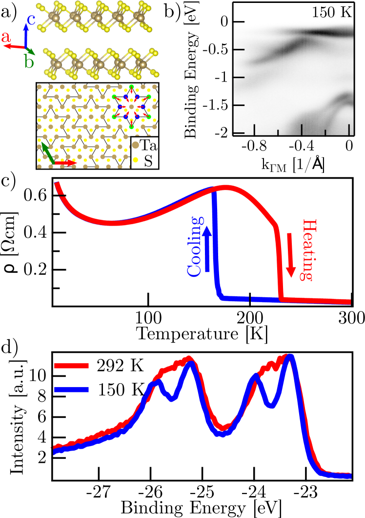
Results. To verify that our samples do not show any macroscopic differences to previously studied 1T-TaS2 samples and that our findings are therefore generally applicable to 1T-TaS2 samples, we have performed several characterisation measurements, the results of which are presented in figures 1b)-d). Figure 1b) shows a representative ARPES image obtained with a photon energy of 21.2 eV at a temperature of 150 K, along the direction of the surface Brioullin zone. The dispersion is in good agreement with previous ARPES measurements of 1T-TaS2 in the CCDW phase [28, 29, 27]. Figure 1c) display XPS spectra of the Ta 4f core levels at room temperature and 150 K i.e. above and below the CCDW phase transition temperature. The two peak structure is expected due to the CDW creating two inequivalent Ta sites on the outer and inner ring of the SoD structure [30]. The enhanced peak splitting observed below the CCDW transition temperature is ascribed to a stronger CDW amplitude after the transition [30]. Overall, these findings are in agreement with previous XPS measurements [30, 31]. Figure 1d) presents resistivity as a function of temperature. The jump in resistivity occurs at the near commensurate to commensurate phase transition at around 165 K upon cooling as expected from previous studies [32, 27] and agrees with observations from temperature dependent ARPES measurements in which we find a similar transition temperature. Additional characterisation measurements can be found in the supplementary material and also show no unusual behaviour. In summary, we find that our samples macroscopically behave as expected from previous literature using the above characterisation techniques.
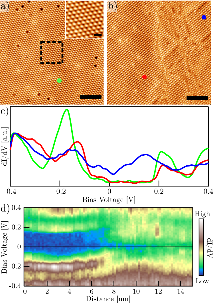
Figure 2a) shows an STM image of the surface of TaS2 taken with a gap voltage of -0.4 V. The inset presents a magnified section of the main image, indicated by the dashed square. In both the main image and the inset, the bright spots forming the periodic lattice correspond to individual SoDs in the CDW phase and not to individual surface atoms. The appearance of the surface is as expected from previous observations on 1T-TaS2 in the CCDW phase with the SoDs aligned in a hexagonal lattice. However, our images contain an increased number of dark defect sites as compared to literature which we will discuss later. In contrast, Figure 2b) is another image of the TaS2 surface taken on the same cleave surface as Figure 2a) without any intervening treatment of the sample and measured within hours of the image in Figure 2a). Notably, the surface on the right side of the image is filled with a dense network of domain walls, as seen in the pulse-induced mosaic phase previously described in TaS2 [13, 26, 15]. Additionally, there appears to be a variation in intensity at or near the transition between the regular and mosaic regions of the image. This contrast is again strongly reminiscent of both the pulse induced mosaic phase, see for example Figure 2 in Ref. [26].
In Figure 2c) we compare STS spectra obtained at three different points in Figures 2a) and b) as marked by dots of the corresponding color. While the spectra taken at points on the non-mosaic part of the surface are gapped as expected for the CCDW phase, the blue spectrum taken within a domain of the mosaic region is metallic, as for the pulse induced mosaic. Further STS measurements, presented in the supplementary materials, obtained at different locations in Figure 2b) confirm that the visual contrast between the normal and mosaic phase consistently coincides with a change in the electronic behaviour from insulating to metallic. To further verify whether this naturally occurring mosaic behaves the same electronically as the pulse induced mosaic, Figure 2d) contains a cut across an STS map taken across the boundary between the normal and metallic mosaic phases which agrees very well with data previously obtained for the pulse induced mosaic phase [26]. In particular, the shifting of the peak at -0.2 V towards the Fermi level and an accompanying shift of the gap into the unoccupied states is very similar to the pulse induced mosaic phase.
We will now focus on the immediate origins of the metallic behaviour in the mosaic phase, starting from the hypothesis that a change of stacking of the top layer to AB stacking due to the presence of domain walls in only one of the top two layers is responsible for this metalicity. Using the assumption that the periodicity of the CDW in the second-to-top layer remains the same, that is to say, there is not coincidentally also a domain wall at the same location in the second-to-top layer, and knowing what stacking order is present in the normal insulating phase, one can reconstruct the stacking order in the metallic phase by extrapolating the lattice of one domain across the domain wall and comparing it to the lattice in a second domain. When then comparing the shift between the two lattices with the offsets between Ta atoms in the regular atomic lattice, we can gain information about which shift has occurred across the domain wall and thus how the stacking changes. Further technical details of the analysis process can be found in the supplementary material.
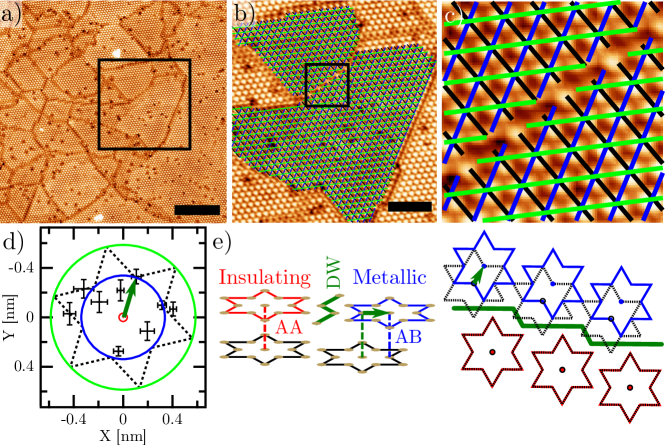
We apply this method to the image in Figure 3a) which has several large domains with differing electronic character adjacent to each other, as seen from the visual contrast between the slightly darker metallic mosaic regions and the brighter insulating normal phase, which makes it suitable for our method of analysis. We assume that the normal phase in this image is AA stacked, due to the contrast between the insulating and metallic domains which is the same as in figure 2b) which shows a large gap characteristic of this termination [24, 33]. Additionally, we have also observed a metallic mosaic on an AC stacked top layer, which shows a strikingly different contrast, as presented in the supplementary materials. Figure 3b) contains a zoom on two domains of different electronic character with fits applied along the three axes of the hexagonal CDW lattice represented by the coloured lines. A further zoom onto the region around the domain wall is shown in Figure 3c). Here, the change of periodicity between the two domains can be seen by eye when comparing the lines along the same lattice directions on either side of the domain wall. Finally, the result of the analysis is presented in Figure 3d). The lattice shift between a total of nine sets of two adjacent domains each with different electronic character is indicated by the black crosses. In essence, the black crosses represent the center positions of the SoDs of a metallic domain with respect to the center of the SoDs in an adjacent insulating domain. The blue and green circles mark the distances of the inner Ta atoms of the SoDs (corresponding to an AB stacking order) and outer Ta atoms (corresponding to AC stacking) respectively while the red circled dot corresponds to AA stacking. The obtained shifts thus agree with the shift leading to an AB stacking in the metallic domains, providing support for a non-bulk stacking related origin of the metallicity of the mosaic phase only from knowledge about the top layer.
Figure 3e) presents a schematic explanation of how this shift occurs. On the left, two layers of Ta atoms as well as the outline of the SoD CDW pattern can be seen. On the left side of the domain wall, the top layer is stacked in the AA configuration and thus displays the expected insulating behaviour. However, on the transition across the domain wall in the top layer, the phase of the top layer CDW changes with respect to that of the second-to-top layer since the domain wall is composed of Ta atoms not participating in the formation of any complete SoDs. Again, we assume here that no domain wall is occurring in the second-to-top layer at the same location. While domain walls in the second-to-top layer have been indirectly observed both in previous studies and in our own measurements [24, 15, 26], there is no reason to assume that they consistently occur in the same pattern as the ones in the top layer. As such, a spatial shift between the centres of the top and second-to-top layer CDW occurs, indicated by the green arrow, thus altering the stacking order. The right panel provides a top-down view of the same situation with the second-to-top layer SoDs being indicated by dashed black lines. In the insulating phase on the bottom, the SoDs overlap between the two layers whereas in the metallic phase, the AB stacking order occurs due to the broken periodicity in the top layer caused by the domain wall, while the periodicity of the bottom layer CDW is maintained as no domain wall occurs in that layer. The shift which we have calculated for several domain walls in Figure 3d) is again represented by a green arrow in the top domain. Note that this same mechanism also allows for domain walls in the second-to-top layer, with no corresponding domain wall in the top layer, to change the stacking order within a single top layer domain. An example of this occurring can be seen just above and to the right of the center of Figure 2b) where a visual contrast and a change in electronic behaviour occurs between the upper and lower parts of a single top layer domain.
We can further consider that the atomic lattice can only be aligned in two mirror symmetric ways relative to the CDW lattice. These two potential orientations of the atomic lattice are normally indistinguishable from knowledge of only the CDW lattice. However, as the structure of the CDW is not altered by lattice shifts, that is to say the shifted center of the SoD will nevertheless correspond to the location of a Ta atom, the obtained shifts should be located at the Ta locations of one of the two possible atomic lattices. From our analysis, we find that the shifts indeed align reasonably well with one potential atomic lattice as indicated by the dotted black star in 3e). For reference, the second possible atomic lattice based on the CDW lattice would be rotated by thirty degrees around the center of the SoD, meaning the atoms would be located on the same circles in Figure 3d) but centred between the atoms of the chosen lattice. This would correspond less well with our results. Therefore, our analysis is potentially capable of extracting information about the underlying atomic lattice from the behaviour of the CDW across domain walls, even without an image with atomic resolution.
We stress here that this natural mosaic phase has been observed across numerous samples, cleaves and macroscopically distinct locations on the surface of samples from different growth batches and produced by two different sample growers, each time accompanied by a closing of the electronic gap and a visual contrast between the two phases. We have also observed the mosaic phase after various periods of time after cleaving the sample, including in the very first measurement. Its appearance is therefore not likely to be related to sample ageing. Furthermore, while the metallic mosaic phase is sometimes confined to small areas of 1010 nm2, we also observe continuous mosaic regions extending over several hundreds of nanometres and covering a similar fraction of imaged surface area as the insulating normal phase. When selecting different measurement locations on the surface of the same sample we have also noted that on multiple occasions, all measured locations within an area of 1 mm2 on the sample surface contained a metallic mosaic while other areas of the sample only showed the normal insulating phase. Additional STM and STS measurements demonstrating the above can be found in the supplementary material. Given this, we attribute the appearance of this phase in our samples to a sample-intrinsic property which occurs with some significant frequency across TaS2 samples.
We now turn to the question of why this mosaic phase appears in our samples without the need for external stimulation, in contrast to previous studies. As mentioned above, the most immediately striking difference seen in our samples as compared to those in previous studies [24, 26, 15] is the larger amount of intrinsic defects in the CDW lattice, as seen for example in Figure 3a). To quantify this, we determined the number of defects in several STM images taken on samples which hosted the mosaic phase and found that an average of 2.90.4 of surface SoDs contained a defect in these images. In comparison, this value is over twice that of the highest density of such defects found in the existing literature [24, 26, 15]. Even more interestingly, recent investigations of Ti doped TaS2 have also demonstrated the appearance of a metallic mosaic phase at low doping [33]. The density of Ti intercalation defects at the surface on which the mosaic phase is observed is 4.2 of surface SoDs, similar to our results, though from the bulk doping of 1 one would expect 12 of SoDs to show defects. Note that the highest density of surface defects in our measurements remains below the minimum doping reported in ref. [33] for which only changes to the CCDW transition temperature and minor changes to the electronic structure are observed. This is further confirmed by the CCDW transition temperature in our samples which is the same as for pristine samples, see Figure 1d). Thus, in spite of the density of defects in our samples being higher than in previous studies, this does not impact the macroscopic properties of our samples. The defect density in our samples is also far removed from the doping level at which the insulating CDW phase is fully suppressed (8 Ti doping) [33, 34], in agreement with our observations.
One potential explanation for this behaviour is the pinning of domain walls at defects sites during the cooling from the near commensurate CDW phase to the CCDW phase. Though possible, the domain walls which exist in the NCCDW phase are qualitatively different from those in the CCDW phase and it is not obvious how one would directly turn into the other while pinned [35]. There is a different possible non-pinning related explanation for the relationship between defects and the mosaic phase based on theoretical work aimed at explaining the origin of the pulse-induced mosaic in TaS2 [36]. From simulations, it was found that charged defects introduced into a hexagonal lattice lead to the formation of networks of charged, one dimensional domain walls. As such, it appears plausible that the increased density of defects at the surface of our samples causes the formation of a dense network of domain walls, giving rise to the characteristic appearance of the mosaic phase in the same manner as for intentional doping of the sample [33]. The resulting high density of domain walls increases the probability of a domain wall occurring only in one of the top two layers, thus leading to the appearance of the metallic phase in the mosaic due to a change in stacking of the top layer as shown above. However, it is not clear why the majority of domains within the domain wall network would adopt this non-bulk stacking. It may be possible that instead the formation of domain walls due to the effects of intrinsic defects upon cooling is favoured within regions of altered stacking. These findings also provide insight into a potential mechanism of the creation of the pulse-induced mosaic phase, namely that the pulses create similar charged defects in the CDW lattice, which then cause the formation of domain walls as the lattice cools again [14].
In conclusion, we have shown the occurrence of a metallic mosaic phase at the surface of 1T-TaS2 without the need for external stimulation through laser or electrical pulses. Our characterisation of this phase reveals that it behaves the same as the pulse induced phase, leading us to assume that they are the same and opening up the possibilities for study of this phase without the need for additional preparation steps. In analogy with the behaviour of Ti doped TaS2 samples and supported by previous model calculations, we suggest that the origin of the mosaic phase in our samples is found in a higher density of surface defects which lead to the formation of a network of domain walls. Through further analysis of our measurements, we have demonstrated how interlayer stacking could plausibly be changed within the metallic surface domains due to the occurrence of domain walls in only one of the two top layers, which is made more likely by the presence of a large number of domain walls in the mosaic phase. This mechanism can also serve as an explanation for the pulse-induced mosaic phase if one assumes that localised charged defects are created in the CDW lattice by the pulses.
Acknowledgements B.S. and C.M. acknowledge support from the Swiss National Science Foundation Grant No. P00P2170597.
References
- Novoselov et al. [2004] K. S. Novoselov, A. K. Geim, S. V. Morozov, D. Jiang, Y. Zhang, S. V. Dubonos, I. V. Grigorieva, and A. A. Firsov, Electric field effect in atomically thin carbon films, Science 306, 666 (2004).
- Li et al. [2014] L. Li, Y. Yu, G. J. Ye, Q. Ge, X. Ou, H. Wu, D. Feng, X. H. Chen, and Y. Zhang, Black phosphorus field-effect transistors, Nature Nanotechnology 9, 372 (2014).
- Chen et al. [2018] Y. Chen, Y. Sun, J. Peng, J. Tang, K. Zheng, and Z. Liang, 2D Ruddlesden-Popper perovskites for optoelectronics, Advanced Materials 30, 1703487 (2018).
- Yan et al. [2018] J. Yan, W. Qiu, G. Wu, P. Heremans, and H. Chen, Recent progress in 2D/quasi-2D layered metal halide perovskites for solar cells, Journal of Materials Chemistry A 6, 11063 (2018).
- Zhou et al. [2018] X. Zhou, X. Hu, S. Zhou, H. Song, Q. Zhang, L. Pi, L. Li, H. Li, J. Lü, and T. Zhai, Tunneling diode based on WSe2/SnS2 heterostructure incorporating high detectivity and responsivity, Advanced Materials 30, 1703286 (2018).
- Wang et al. [2012] Q. H. Wang, K. Kalantar-Zadeh, A. Kis, J. N. Coleman, and M. S. Strano, Electronics and optoelectronics of two-dimensional transition metal dichalcogenides, Nature Nanotechnology 7, 699 (2012).
- Keum et al. [2015] D. H. Keum, S. Cho, J. H. Kim, D.-H. Choe, H.-J. Sung, M. Kan, H. Kang, J.-Y. Hwang, S. W. Kim, H. Yang, et al., Bandgap opening in few-layered monoclinic MoTe2, Nature Physics 11, 482 (2015).
- Wang et al. [2018] G. Wang, L. Li, W. Fan, R. Wang, S. Zhou, J.-T. Lü, L. Gan, and T. Zhai, Interlayer coupling induced infrared response in WS2/MoS2 heterostructures enhanced by surface plasmon resonance, Advanced Functional Materials 28, 1800339 (2018).
- Bhattacharyya and Singh [2012] S. Bhattacharyya and A. K. Singh, Semiconductor-metal transition in semiconducting bilayer sheets of transition-metal dichalcogenides, Physical Review B 86, 075454 (2012).
- Hong et al. [2017] J. Hong, C. Wang, H. Liu, X. Ren, J. Chen, G. Wang, J. Jia, M. Xie, C. Jin, W. Ji, et al., Inversion domain boundary induced stacking and bandstructure diversity in bilayer MoSe2, Nano Letters 17, 6653 (2017).
- Wu and Lieber [1989] X. L. Wu and C. M. Lieber, Hexagonal domain-like charge density wave phase of TaS2 determined by scanning tunneling microscopy, Science 243, 1703 (1989).
- Scruby et al. [1975] C. Scruby, P. Williams, and G. Parry, The role of charge density waves in structural transformations of 1-TaS2, Philosophical Magazine 31, 255 (1975).
- Stojchevska et al. [2014] L. Stojchevska, I. Vaskivskyi, T. Mertelj, P. Kusar, D. Svetin, S. Brazovskii, and D. Mihailovic, Ultrafast switching to a stable hidden topologically protected quantum state in an electronic crystal, Science 344, 177 (2014).
- Stahl et al. [2020] Q. Stahl, M. Kusch, F. Heinsch, G. Garbarino, N. Kretzschmar, K. Hanff, K. Rossnagel, J. Geck, and T. Ritschel, Collapse of layer dimerization in the photo-induced hidden state of 1t-tas2, Nature Communications 11, 1247 (2020).
- Cho et al. [2016] D. Cho, S. Cheon, K.-S. Kim, S.-H. Lee, Y.-H. Cho, S.-W. Cheong, and H. W. Yeom, Nanoscale manipulation of the Mott insulating state coupled to charge order in 1T-TaS2, Nature Communications 7, 1 (2016).
- Hollander et al. [2015] M. J. Hollander, Y. Liu, W.-J. Lu, L.-J. Li, Y.-P. Sun, J. A. Robinson, and S. Datta, Electrically driven reversible insulator–metal phase transition in 1-TaS2, Nano Letters 15, 1861 (2015).
- Vaskivskyi et al. [2016] I. Vaskivskyi, I. Mihailovic, S. Brazovskii, J. Gospodaric, T. Mertelj, D. Svetin, P. Sutar, and D. Mihailovic, Fast electronic resistance switching involving hidden charge density wave states, Nature Communications 7, 1 (2016).
- Ravnik et al. [2021] J. Ravnik, M. Diego, Y. Gerasimenko, Y. Vaskivskyi, I. Vaskivskyi, T. Mertelj, J. Vodeb, and D. Mihailovic, A time-domain phase diagram of metastable states in a charge ordered quantum material, Nature Communications 12, 1 (2021).
- Wu et al. [2022] Z. Wu, K. Bu, W. Zhang, Y. Fei, Y. Zheng, J. Gao, X. Luo, Z. Liu, Y.-P. Sun, and Y. Yin, Effect of stacking order on the electronic state of 1-TaS2, Physical Review B 105, 035109 (2022).
- Nicholson et al. [2022] C. W. Nicholson, F. Petocchi, B. Salzmann, C. Witteveen, M. Rumo, G. Kremer, F. O. von Rohr, P. Werner, and C. Monney, Modified interlayer stacking and insulator to correlated-metal transition driven by uniaxial strain in 1T-TaS2, arXiv preprint arXiv:2204.05598 (2022).
- Endo et al. [2000] T. Endo, S. Nakao, W. Yamaguchi, T. Hasegawa, and K. Kitazawa, Influence of CDW stacking disorder on metal–insulator transition in 1-TaS2, Solid State Communications 116, 47 (2000).
- Hovden et al. [2016] R. Hovden, A. W. Tsen, P. Liu, B. H. Savitzky, I. El Baggari, Y. Liu, W. Lu, Y. Sun, P. Kim, A. N. Pasupathy, et al., Atomic lattice disorder in charge-density-wave phases of exfoliated dichalcogenides (1-TaS2), Proceedings of the National Academy of Sciences 113, 11420 (2016).
- Ritschel et al. [2018] T. Ritschel, H. Berger, and J. Geck, Stacking-driven gap formation in layered 1-TaS2, Physical Review B 98, 195134 (2018).
- Butler et al. [2020] C. Butler, M. Yoshida, T. Hanaguri, and Y. Iwasa, Mottness versus unit-cell doubling as the driver of the insulating state in 1-TaS2, Nature Communications 11, 1 (2020).
- Petocchi et al. [2022] F. Petocchi, C. W. Nicholson, B. Salzmann, D. Pasquier, O. V. Yazyev, C. Monney, and P. Werner, Mott versus hybridization gap in the low-temperature phase of 1T-TaS2, arXiv preprint arXiv:2202.01285 (2022).
- Ma et al. [2016] L. Ma, C. Ye, Y. Yu, X. F. Lu, X. Niu, S. Kim, D. Feng, D. Tománek, Y.-W. Son, X. H. Chen, et al., A metallic mosaic phase and the origin of Mott-insulating state in 1-TaS2, Nature Communications 7, 1 (2016).
- Wang et al. [2020] Y. Wang, W. Yao, Z. Xin, T. Han, Z. Wang, L. Chen, C. Cai, Y. Li, and Y. Zhang, Band insulator to Mott insulator transition in 1-TaS2, Nature Communications 11, 1 (2020).
- Perfetti et al. [2005] L. Perfetti, T. A. Gloor, F. Mila, H. Berger, and M. Grioni, Unexpected periodicity in the quasi-two-dimensional Mott insulator 1-TaS2 revealed by angle-resolved photoemission, Physical Review B 71, 153101 (2005).
- Ngankeu et al. [2017] A. S. Ngankeu, S. K. Mahatha, K. Guilloy, M. Bianchi, C. E. Sanders, K. Hanff, K. Rossnagel, J. A. Miwa, C. B. Nielsen, M. Bremholm, et al., Quasi-one-dimensional metallic band dispersion in the commensurate charge density wave of 1-TaS2, Physical Review B 96, 195147 (2017).
- Hughes and Scarfe [1995] H. P. Hughes and J. A. Scarfe, Site specific photohole screening in a charge density wave, Physical Review Letters 74, 3069 (1995).
- Hellmann et al. [2010] S. Hellmann, M. Beye, C. Sohrt, T. Rohwer, F. Sorgenfrei, H. Redlin, M. Kalläne, M. Marczynski-Bühlow, F. Hennies, M. Bauer, et al., Ultrafast Melting of a Charge-Density Wave in the Mott Insulator 1-TaS2, Physical Review Letters 105, 187401 (2010).
- Sipos et al. [2008] B. Sipos, A. F. Kusmartseva, A. Akrap, H. Berger, L. Forró, and E. Tutiš, From Mott state to superconductivity in 1-TaS2, Nature Materials 7, 960 (2008).
- Zhang et al. [2022] W. Zhang, J. Gao, L. Cheng, K. Bu, Z. Wu, Y. Fei, Y. Zheng, L. Wang, F. Li, X. Luo, et al., Visualizing the evolution from Mott insulator to Anderson insulator in Ti-doped 1-TaS2, NPJ Quantum Materials 7, 1 (2022).
- Gao et al. [2021] J. Gao, W. Zhang, J. Si, X. Luo, J. Yan, Z. Jiang, W. Wang, H. Lv, P. Tong, W. Song, et al., Chiral charge density waves induced by Ti-doping in 1-TaS2, Applied Physics Letters 118, 213105 (2021).
- Park et al. [2019] J. W. Park, G. Y. Cho, J. Lee, and H. W. Yeom, Emergent honeycomb network of topological excitations in correlated charge density wave, Nature Communications 10, 4038 (2019).
- Karpov and Brazovskii [2018] P. Karpov and S. Brazovskii, Modeling of networks and globules of charged domain walls observed in pump and pulse induced states, Scientific Reports 8, 1 (2018).