High-performance microresonator optical parametric oscillator on a silicon chip
Abstract
Optical parametric oscillation (OPO) is distinguished by its wavelength access, that is, the ability to flexibly generate coherent light at wavelengths that are dramatically different from the pump laser, and in principle bounded solely by energy conservation between the input pump field and the output signal/idler fields. As society adopts advanced tools in quantum information science, metrology, and sensing, microchip OPO may provide an important path for accessing relevant wavelengths. However, a practical source of coherent light should additionally have high conversion efficiency and high output power. Here, we demonstrate a silicon photonics OPO device with unprecedented performance. Our OPO device, based on the third-order () nonlinearity in a silicon nitride microresonator, produces output signal and idler fields widely separated from each other in frequency (150 THz), and exhibits a pump-to-idler conversion efficiency up to 29 with a corresponding output idler power of 18 mW on-chip. This performance is achieved by suppressing competitive processes and by strongly overcoupling the output light. This methodology can be readily applied to existing silicon photonics platforms with heterogeneously-integrated pump lasers, enabling flexible coherent light generation across a broad range of wavelengths with high output power and efficiency.
Many applications in quantum information science, metrology, and sensing require access to coherent laser light at a variety of wavelengths, ideally in a chip-integrated format suitable for scalable fabrication and deployment. While integrated photonics lasers are highly developed in the telecommunications band malik_low_2021 , many of the aforementioned technologies operate at other wavelengths. To this end, the extension of heterogeneously integrated lasers to other bands has been pursued, with recent demonstrations at 980 nm park_heterogeneous_2020 ; tran_extending_2021 and 2000 nm spott_heterogeneous_2017 . However, wavelength access across the entirety of a broad spectral range would demand the challenging integration of several material platforms. In contrast, table-top nonlinear optics boyd_nonlinear_2010 ; agrawal_nonlinear_2013 is widely used to produce coherent light at wavelengths that are difficult to access through direct laser emission. Processes such as optical harmonic generation, stimulated four-wave mixing, and optical parametric oscillation enable the spectral translation and/or generation of coherent light at wavelength(s) that can differ dramatically from those at the input. The development of high-performance nonlinear integrated photonics platforms moss_new_2013 , when combined with compact lasers, may provide a compelling approach for realizing flexible wavelength access on-chip.
Here, we demonstrate high-performance OPO on a silicon microchip. By suppressing competing nonlinear processes that would otherwise saturate parametric gain and by strongly overcoupling the output mode while retaining high overall , we simultaneously realize wide spectral separation between the participating modes (signal-idler separation 150 THz), high conversion efficiency (up to ), and useful output power (up to 21 mW), a compelling combination of properties that, to the best of our knowledge, have not previously been simultaneously achieved in on-chip OPO. Our work highlights the potential of OPO in silicon photonics to address many requirements for deployable laser technologies in scientific applications, particularly in light of recent progress on heterogeneous integration of III-V lasers and silicon nonlinear photonics xiang_laser_2021 .
Requirements for high performance
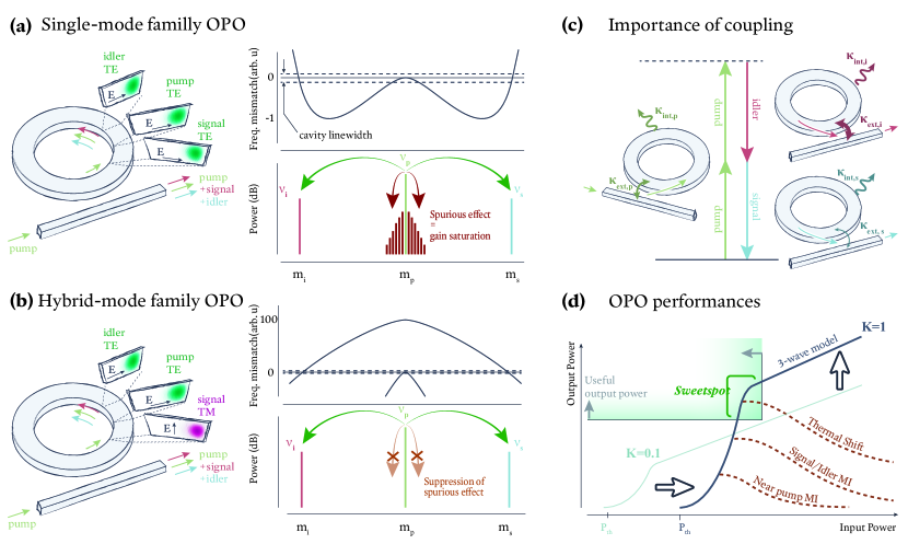
In a OPO, pump photons at are converted to up-shifted signal photons (, with ) and down-shifted idler photons (, with ) that satisfy energy conservation (2 = + ). Appreciable conversion efficiency requires phase-matching, so that where is the propagation constant for the pump, signal, and idler modes, respectively. In microring resonators, which have periodic boundary conditions, this phase relationship can be recast as where denotes the azimuthal mode order of the pump, signal, and idler modes respectively. Finally, OPO has a power threshold, meaning that the cavity modes must have sufficiently low loss rates (high loaded ) that can be exceeded by the available parametric gain. While phase- and frequency-matching and high- are baseline requirements for OPO, additional requirements are imposed if high-performance OPO is to be achieved. First, it is necessary to suppress competitive nonlinear processes that, for example, divert pump energy to the creation of frequency components other than the targeted signal and idler frequencies (Fig. 1(a)-(b)). In addition, to maximize the conversion efficiency for the output field of interest, optimization of the pump injection into the microring and output extraction from the microring is needed (Fig. 1(c)). We discuss each of these items below, starting with resonator-waveguide coupling.
Increasing the maximum conversion efficiency
The conversion efficiency for the signal (or idler) is dependent on the coupling regime (e.g., overcoupled/undercoupled) of both the signal (or idler) and the pump sayson_octave-spanning_2019 ; stone_conversion_2022 . As a starting point, we consider a simplified three-mode model in which only the pump, signal, and idler modes are allowed to interact, from which the system’s maximum conversion efficiency, can be derived sayson_octave-spanning_2019 . Here, is the flux of pump photons at the input of the waveguide and is flux of signal or idler photons at the output of the waveguide. The maximum conversion efficiency, , will occur when the Kerr-shifted modes are perfectly phase- and frequency-matched, and can be written in terms of the coupling parameter of each resonance as:
| (1) |
where and is the extrinsic (waveguide coupling) or intrinsic loss rate for the pump, signal, or idler mode (Fig. 1(c)). This equation shows that in a OPO increases to a maximum value of 0.5 as increases without bound. However, strongly overcoupling the resonator decreases the total of the corresponding cavity mode(s), yielding a less efficient nonlinear enhancement. This can translate into very high threshold powers which may be unsupportable by compact pump lasers. Therefore, efficient OPO generation via overcoupling requires a resonator with very high intrinsic as a starting point. In recent years, it has been demonstrated that Si3N4 microring resonators, suitable for nonlinear photonics and created by mass-production fabrication techniques, can yield intrinsic liu_high-yield_2021 , suggesting that strong overcoupling can be reached while maintaining high overall .
Suppressing parasitic processes
In practice, saturation of OPO usually occurs before is reached, especially when imposing the additional requirement of achieving with high output power. In OPO, the frequency mismatch between the cold-cavity resonances is compensated by their Kerr shifts, which are pump-power dependent quantities, so that there is a limited range of input powers for which will be small enough for high conversion efficiency to be achieved sayson_octave-spanning_2019 ; stone_conversion_2022 . Thermorefractive shifts will typically also play a role, and in widely-separated OPO the wavelength-dependence of the thermorefractive shifts also becomes meaningful. However, because dispersion is influenced by device geometry lu_milliwatt-threshold_2019 , these effects can be addressed by choosing a geometry that targets a compatible with the input power range of interest.
A more significant challenge comes from parasitic nonlinear processes that deplete the gain of the desired OPO process (Fig. 1(a)-(b)). Competitive parasitic nonlinear processes in this system are a consequence of a microring resonator’s many azimuthal spatial modes stone_conversion_2022 , and can be worsened by the presence of higher-order transverse spatial modes (including those of a different polarization). As a result, in widely-separated OPO, there can be hundreds of modes that exist between the pump and targeted signal (or idler) mode, which can be populated by processes such as modulational instability and subsequent Kerr comb formation. These processes are detrimental to system efficiency as they divert pump photons away from the targeted three-mode OPO process. The natural way to limit close-to-pump parasitic nonlinear processes is to situate the pump in the normal dispersion regime, so that Kerr shifts lead to a larger amount of frequency mismatch for nearby signal-idler pairs. However, normal dispersion around the pump (i.e., ) must be balanced by sufficient higher-order dispersion for the widely-separated signal-idler pair of interest to be frequency matched, so that , as in (Fig. 1(a)) lin_proposal_2008 ; lu_milliwatt-threshold_2019 ; sayson_octave-spanning_2019 . However, the amount of normal dispersion near the pump is also important, as cross-phase modulation involving the widely-separated signal and idler modes can result in nonlinear conversion to unwanted spectral channels near the pump if the amount of normal dispersion is insufficient stone_conversion_2022 . Thus a dichotomy arises: strong normal dispersion suppresses parasitic process, but strong normal dispersion makes the frequency and phase matching conditions challenging to satisfy.
This problem is circumvented though the use of hybrid-mode OPO (hOPO) zhou_hybrid-mode-family_2021 , which phase and frequency matches azimuthal modes from different transverse spatial mode families (Fig. 1(b)). Using this technique, it is possible for each of the pump, signal, and idler bands to have strong normal dispersion, thereby suppressing competitive processes, while maintaining phase and frequency matching for the targeted modes. Hence, through careful design of the resonator’s dispersion, it is possible to isolate the hOPO, taking the many-mode system to the limit where it behaves like the modeled three-mode system, where high output power and high conversion efficiency are simultaneously accessible without sacrificing wavelength access.
Device design, dispersion, and coupling
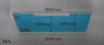
Our devices were fabricated by Ligentec NIST_disclaimer through a photonic damascene process liu_high-yield_2021 and consist of an 890 nm thick, fully SiO2-clad Si3N4 microring resonator with outer radius of 23 m and a ring width of m. Figure 2(a) shows a typical cross-section of a microring, which has an inverted trapezoidal shape, with sidewall angle as a result of the reflow step within the damascene process, and whose geometry has been verified through focused ion beam cross-sectional imaging of the devices (see Supplementary Material Fig. S2).
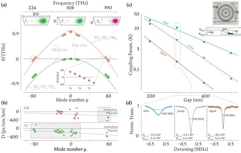
We first measure the frequency mismatch for phase-matched sets of signal, idler, and pump modes, as shown in Fig. 2(a) (see Methods). We plot as a function of the relative mode number , indexed with respect to a pump band mode at 308 THz. We consider two cases, the targeted process in which the idler and pump are from the fundamental transverse electric (TE0) mode family and the signal is from the fundamental transverse magnetic mode (TM0) family (shown in purple), and one in which all three modes are from the TE0 mode family (shown in green), i.e., the more typical single mode family case. In the TE0-TE0-TM0 hOPO scheme, at frequencies near 390 THz and 226 THz, indicating that we can anticipate an OPO signal and idler pair near these frequencies for an appropriate level of pump laser detuning and Kerr nonlinear shifts to compensate for any non-zero frequency mismatch. In contrast, at all frequencies for the TE0-TE0-TE0 case, indicating that the widely separated process of interest will not occur for this set of modes. More importantly, these results confirm that the pump is situated in a regime of normal dispersion, which is explicitly validated through the evaluation of the dispersion parameter for the TE0 and TM0 mode families, where . As shown in Fig. 2(b), for the TE0 family - not only in the pump band, but also in the idler band (as well as the signal band). In addition, for the TM0 family in the signal band. As discussed above, this normal dispersion throughout the entire frequency range between the signal and idler, and in particular surrounding the pump, should suppress many potentially competing nonlinear processes.
We next move to the resonator-waveguide coupling, which, as noted in the previous section, is critical for a high-performance OPO. We focus on conversion efficiency and output power of the idler generated near 1300 nm. From Eq. (1), depends on the coupling parameter for the pump and for the idler , with greater efficiency being achieved with increased and . Additionally, to maintain an acceptable threshold power and because we are not focusing on extraction of the signal, we target small . Using a straight waveguide that is at a gap and tangent to the ring naturally leads to variation in resonator-waveguide coupling across broad spectral ranges, since the modal overlap between ring and waveguide modes depends on the evanescent decay lengths of each mode, which itself depends on wavelength. As a result, long wavelength modes tend to be overcoupled and short wavelength modes tend to be undercoupled moille_broadband_2019 , so that as desired, provided that intrinsic quality factors remain high throughout.
To investigate further, we experimentally study , , and for a series of devices in which the resonator-waveguide gap is varied between 200 nm and 500 nm in Fig. 2(c). We observe the expected increase in with decreasing gap, that throughout, and that specific gap values can be chosen to target the high-performance overcoupled regime. For example, Fig. 2(d) shows the cavity mode transmission spectra at a gap of 300 nm. Of note are the high intrinsic quality factors achieved, e.g., for the signal, pump, and idler bands, respectively. This enables significant overcoupling to be achieved (, ) while maintaining high overall s. In comparison to other works utilizing resonators of a similar cross-section and size (i.e., an FSR of 1 THz) ji_methods_2021 , the intrinsic s we observe are somewhat higher. This is likely a consequence of the relatively wide 3 m ring widths we use, which limits the interaction of the optical field with the sidewalls. The ability to use such wide rings is a consequence of the hOPO scheme.
High-performance OPO
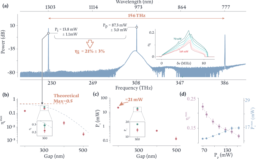
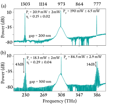
We next characterize the hOPO performance of our dispersion- and coupling-engineered microresonators. Figure 3(a) shows the output spectrum when a device with a gap of 300 nm is pumped with mW of power at a frequency of 308 THz. Because parasitic sidebands are suppressed, a well-isolated OPO spectrum with idler at 230 THz and signal at 386 THz is produced with an on-chip idler power of mW, corresponding to a conversion efficiency (in photon flux) (the uncertainty values are described in the Fig. 3 caption). In contrast, traditional wide-span single-mode-family OPOs typically start to see the formation of parasitic sidebands at 1 mW. To elucidate the crucial role of resonator-waveguide coupling in the generation of high and high OPO, Fig. 3(b)-(c) plots these metrics as a function of resonator-waveguide gap, illustrating a strong increase in both as the resonator-waveguide gap decreases (and therefore as the increase; see Fig. 2(c)). based on Eq. (1) and the values from Fig. 2(c) are plotted as a dashed line in Fig. 3(b). In general, the measured values we report are still below the theoretical curve, likely due to imperfect frequency matching, where the pump detuning, Kerr, and thermal shifts do not perfectly compensate for . In Fig. 3(c) we note that at smallest gap, we can generate isolated OPO with nearly 21 mW in the idler field (see Fig. 4(a)) despite some reduction in efficiency (190 mW pump), likely due to the aforementioned imperfect frequency matching. Finally, Fig. 4(b) displays a spectrum with and mW, recorded in Fig. 3(b)-(c) as a green dot at a gap of 300 nm, which is one of the highest conversion efficiencies achievable in our devices. At these levels of and , parasitic sidebands resurface, although the sidebands around the idler are still suppressed by more than 40 dB. Further improvements may be possible with continued device engineering to account for Kerr and thermal-shift contributions to the frequency mismatch.
We further consider the evolution of our OPO output as a function of pump power and pump laser tuning within the pump mode. In Fig. 3(a, inset) we plot a series of traces for waveguide-coupled pump powers between 70 mW and 165 mW, and for each trace we vary the pump laser frequency while recording . The x-axis is referenced to the OPO threshold, that is, for each waveguide-coupled pump power, we adjust the pump laser frequency until the dropped power in the cavity is high enough to reach threshold, and that value is taken as zero detuning. Beyond threshold, each trace displays a steady increase in (and hence ) until a maximum value for each is reached, after which the values decrease and eventually go to zero once frequency matching is completely lost. The detuning value at which this occurs depends on pump power, which is likely due to the differing thermal shifts of the cavity resonances and its impact on frequency mismatch. Once again, the strong normal dispersion for the pump mode family is successful in suppressing close-band parametric process, and pure OPO spectra with isolated pump/signal/idler tones like that in Fig. 3(a) are observed for much of the tuning range, though in some cases, the regions of highest conversion efficiency show additional parametric sidebands, as noted above and shown in Fig. 4(b). The additional sidebands remain strongly suppressed around the idler (40 dB to 50 dB below the idler), while in the signal band, they are only suppressed by 15 dB to 20 dB. Given the normal dispersion around the signal (Fig. 2(b)), the origin of these unwanted sidebands is ambiguous. It is possible that mode couplings result in local regions of near-zero dispersion (e.g., seen in the spread in the dispersion data) that might promote parasitic processes once the signal and/or idler power become sufficiently strong. Finally, Fig. 3(d) shows and for this OPO device as a function of waveguide-coupled pump power. We observe a saturation of and a monotonic reduction in as the pump power increases, likely due to the aforementioned combination of pump-power-dependent frequency mismatch (due to thermal shifts) and competing parasitic processes near the signal and idler bands. Further mitigation of these effects is needed to continue to improve the power performance and conversion efficiency of these devices.
Discussion and context
In considering the potential applications and future development of the OPO devices we describe in this work, it is useful to place their performance in context with other demonstrated OPO systems. Figure 5 illustrates the output power for various OPO demonstrations, ranging from chip-integrated technologies to mm-scale resonators to larger table-top technologies, as a function of their input power. While OPO has seen tremendous progress at all scales, it stands to reason that a widely-deployable on-chip device should have access to an on-chip pump source and produce more than (for example) 1 mW output power. As highlighted by the red gradients in Fig. 5, power considerations alone greatly reduce the number of OPO demonstrations amenable to deployable systems. The additional requirements of small-size and compatibility with silicon photonics leaves our microresonator device as a strong contender for the rapid and scalable deployment of a wide-wavelength-access laser system that simultaneously achieves high output power and conversion efficiency.
We emphasize that while integrated microresonator OPOs have realized high efficiency previously, it has largely been in a regime of low output powers (W), with the exceptions of Refs. bruch_-chip_2019 ; zhou_hybrid-mode-family_2021 , where a few mW of signal and idler power were generated from a 780 nm band pump, but the signal-idler separation was limited to a few tens of THz. Our work realizes output powers exceeding 20 mW at a signal-idler separation greater than 150 THz, while operating with pump powers that are still accessible from compact laser sources. Finally, we note that table-top OPOs routinely produce significantly more than mW of output power at high efficiency, though they require pump powers that are typically not easily available from compact laser sources.
To summarize, we demonstrate high-performance on-chip microresonator optical parametric oscillation that produces mW of output power at conversion efficiencies %, without compromising on the span of the output signal and idler frequencies ( THz signal-idler separation). Simultaneously realizing these three features in an on-chip OPO represents a significant advance in the realization of flexible wavelength access for lasers. Furthermore, its development on a platform compatible with silicon photonics makes it well suited for wide-scale deployment outside of laboratory settings. This was accomplished by suppressing competitive processes within the resonator through the use of an hOPO scheme and by engineering the coupling to an access waveguide. Going forward, we expect combined coupling engineering and flexible frequency matching techniques, such as the hybrid mode-matching scheme used in this work (or recently implemented photonic crystal microring approaches black2022 ; lu_kerr_2022 ), to enable high-performance OPO across different wavelength bands, including the visible lu_-chip_2020 and mid-infrared sayson_octave-spanning_2019 ; tang_widely_2020 . Such work would further establish microresonator OPO as a practical approach for realizing high-performance laser wavelength access across a broad spectral range.
References
- (1) Malik, A. et al. Low noise, tunable silicon photonic lasers. Applied Physics Reviews 8, 031306 (2021).
- (2) Park, H., Zhang, C., Tran, M. A. & Komljenovic, T. Heterogeneous silicon nitride photonics. Optica 7, 336 (2020). URL https://opg.optica.org/abstract.cfm?URI=optica-7-4-336.
- (3) Tran, M. et al. Extending the spectrum of fully integrated photonics. arXiv:2112.02923 [physics] (2021). URL http://arxiv.org/abs/2112.02923.
- (4) Spott, A. et al. Heterogeneous Integration for Mid-infrared Silicon Photonics. IEEE Journal of Selected Topics in Quantum Electronics 23, 1–10 (2017). URL https://ieeexplore.ieee.org/document/7909040/.
- (5) Boyd, R. W. Nonlinear optics (Academic Press : Elsevier, 2010).
- (6) Agrawal, G. P. Nonlinear fiber optics (Elsevier/Academic Press, 2013).
- (7) Moss, D. J., Morandotti, R., Gaeta, A. L. & Lipson, M. New CMOS-compatible platforms based on silicon nitride and Hydex for nonlinear optics. Nature Photonics 7, 597–607 (2013). URL http://www.nature.com/doifinder/10.1038/nphoton.2013.183.
- (8) Xiang, C. et al. Laser soliton microcombs heterogeneously integrated on silicon. Science 373, 99–103 (2021). URL https://www.science.org/doi/10.1126/science.abh2076.
- (9) Sayson, N. L. B. et al. Octave-spanning tunable parametric oscillation in crystalline Kerr microresonators. Nature Photonics 13, 701–706 (2019). URL http://www.nature.com/articles/s41566-019-0485-4.
- (10) Stone, J. R., Moille, G., Lu, X. & Srinivasan, K. Conversion Efficiency in Kerr-Microresonator Optical Parametric Oscillators. Physical Review Applied 17, 024038 (2022). URL https://link.aps.org/doi/10.1103/PhysRevApplied.17.024038.
- (11) Liu, J. et al. High-yield, wafer-scale fabrication of ultralow-loss, dispersion-engineered silicon nitride photonic circuits. Nature Communications 12, 2236 (2021). URL http://www.nature.com/articles/s41467-021-21973-z.
- (12) Lu, X. et al. Milliwatt-threshold visible–telecom optical parametric oscillation using silicon nanophotonics. Optica 6, 1535 (2019). URL https://www.osapublishing.org/abstract.cfm?URI=optica-6-12-1535.
- (13) Lin, Q., Johnson, T. J., Perahia, R., Michael, C. P. & Painter, O. J. A proposal for highly tunable optical parametric oscillation in silicon micro-resonators. Optics Express 16, 10596 (2008). URL https://opg.optica.org/oe/abstract.cfm?uri=oe-16-14-10596.
- (14) Zhou, F. et al. Hybrid-mode-family kerr optical parametric oscillation for robust coherent light generation on chip. Laser & Photonics Reviews 16, 2100582 (2022). URL https://onlinelibrary.wiley.com/doi/abs/10.1002/lpor.202100582.
- (15) Certain commercial products or names are identified to foster understanding. Such identification does not constitute recommendation or endorsement by the National Institute of Standards and Technology, nor is it intended to imply that the products or names identified are necessarily the best available for the purpose.
- (16) Moille, G. et al. Broadband resonator-waveguide coupling for efficient extraction of octave-spanning microcombs. Optics Letters 44, 4737–4740 (2019). URL 2020-07-20.
- (17) Ji, X., Roberts, S., Corato-Zanarella, M. & Lipson, M. Methods to achieve ultra-high quality factor silicon nitride resonators. APL Photonics 6, 071101 (2021). URL https://aip.scitation.org/doi/10.1063/5.0057881.
- (18) Kippenberg, T. J., Spillane, S. M. & Vahala, K. J. Kerr-Nonlinearity Optical Parametric Oscillation in an Ultrahigh- Q Toroid Microcavity. Physical Review Letters 93 (2004). URL http://link.aps.org/doi/10.1103/PhysRevLett.93.083904.
- (19) Marty, G., Combrié, S., Raineri, F. & De Rossi, A. Photonic crystal optical parametric oscillator. Nature Photonics 15, 53–58 (2021). URL http://www.nature.com/articles/s41566-020-00737-z.
- (20) Lu, J. et al. Ultralow-threshold thin-film lithium niobate optical parametric oscillator. Optica 8, 539 (2021). URL https://www.osapublishing.org/abstract.cfm?URI=optica-8-4-539.
- (21) Ledezma, L. et al. Widely-tunable optical parametric oscillator in lithium niobate nanophotonics (2022). eprint arXiv:2203.11482.
- (22) Beckmann, T., Buse, K. & Breunig, I. Optimizing pump threshold and conversion efficiency of whispering gallery optical parametric oscillators by controlled coupling. Optics Letters 37, 5250–5252 (2012).
- (23) Werner, C. S., Buse, K. & Breunig, I. Continuous-wave whispering-gallery optical parametric oscillator for high-resolution spectroscopy. Optics Letters 40, 772 (2015).
- (24) Jia, Y. et al. Continuous-wave whispering-gallery optical parametric oscillator based on CdSiP 2. Optics Express 26, 10833 (2018).
- (25) Ghotbi, M., Esteban-Martin, A. & Ebrahim-Zadeh, M. BiB3O6 femtosecond optical parametric oscillator. Optics Letters 31, 3128–3130 (2006).
- (26) Chaitanya Kumar, S., Das, R., Samanta, G. K. & Ebrahim-Zadeh, M. Optimally-output-coupled, 17.5 W, fiber-laser-pumped continuous-wave optical parametric oscillator. Applied Physics B 102, 31–35 (2011).
- (27) Kumar, S. C. & Ebrahim-Zadeh, M. High-power, fiber-laser-pumped, picosecond optical parametric oscillator based on MgO. Optics Express 19, 26660 (2011).
- (28) Zhu, H. et al. High-efficiency intracavity Nd:YVO4/KTA optical parametric oscillator with 3.6 w output power at 1.53 µm. Optics Express 17, 20669 (2009).
- (29) Haakestad, M. W., Fonnum, H., Arisholm, G., Lippert, E. & Stenersen, K. Mid-infrared optical parametric oscillator synchronously pumped by an erbium-doped fiber laser. Optics Express 18, 25379 (2010).
- (30) Wei, K. et al. Fiber laser pumped high power mid-infrared laser with picosecond pulse bunch output. Optics Express 21, 25364 (2013).
- (31) Liu, J. et al. Highly efficient tunable mid-infrared optical parametric oscillator pumped by a wavelength locked, Q-switched Er. Optics Express 23, 20812 (2015).
- (32) Qijin Mo, Q. M. et al. Widely tunable optical parametric oscillator in periodically poled congruently grown lithium tantalite whispering gallery mode resonators. Chinese Optics Letters 14, 091902–91905 (2016).
- (33) Bruch, A. W., Liu, X., Surya, J. B., Zou, C.-L. & Tang, H. X. On-chip microring optical parametric oscillator. Optica 6, 1361 (2019). URL https://www.osapublishing.org/abstract.cfm?URI=optica-6-10-1361.
- (34) Black, J. A. et al. Tunable lasers with optical-parametric oscillation in photonic-crystal resonators (2022). eprint arXiv:2206.10760.
- (35) Lu, X., Chanana, A., Zhou, F. & Davanco, M. Kerr optical parametric oscillation in a photonic crystal microring for accessing the infrared. Optics Letters 47, 3331–3334 (2022).
- (36) Lu, X., Moille, G., Rao, A., Westly, D. A. & Srinivasan, K. On-chip optical parametric oscillation into the visible. Optica 7, 1417 (2020). URL https://www.osapublishing.org/abstract.cfm?URI=optica-7-10-1417.
- (37) Tang, Y., Gong, Z., Liu, X. & Tang, H. X. Widely separated optical Kerr parametric oscillation in AlN microrings. Optics Letters 45, 1124 (2020). URL https://www.osapublishing.org/abstract.cfm?URI=ol-45-5-1124.
Methods
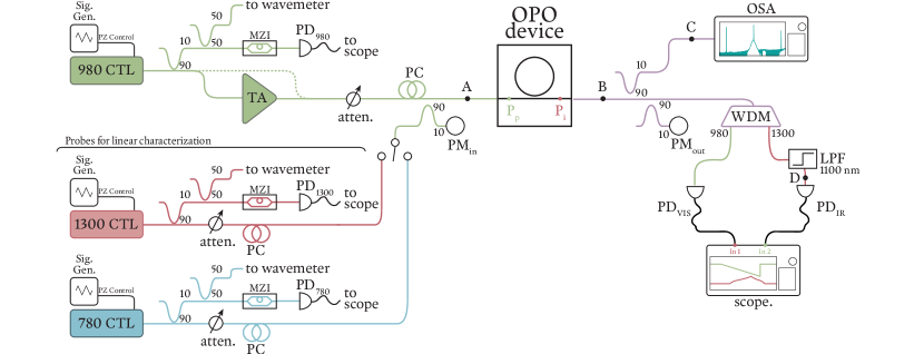
Characterization of OPO devices The OPO devices under study were characterized using the experimental setup shown in Supplementary Fig. S2. For linear characterization of the devices, continuously tunable lasers (CTL) in the 780 nm, 980 nm, and 1300 nm bands were used. Each laser has a piezo-controlled (PZ-controlled) fine-frequency sweep modulated by a signal generator whose voltage is recorded by a data acquisition device (Oscilloscope in drawing). At the output of each laser, cascaded 90/10 and 50/50 couplers (at the appropriate wavelengths) provide light for two frequency measurements. As the PZ control voltage is modulated and recorded, the absolute frequency of the light is measured at the peaks of the driving saw-tooth voltage using a wavemeter. In between the saw teeth, displacements from the wavemeter-referenced frequencies are continuously recorded by Mach-Zehnder interferometers (MZIs) that feed into wavelength-compatible photodiodes. The use of an MZI allows us to track nonlinear deviations in the frequency sweeps of the laser. The 90 % tap of the lasers is then attenuated to low powers (W) using fiber-coupled attenuators (atten.) and aligned to a polarization of interest using fiber-coupled polarization controllers (PCs). Next, 10 % (nominal rating at 980 nm) of the light is tapped to a power meter (PMin) to measure and monitor the power during subsequent steps and measurements. Finally, light is injected into the on-chip waveguide with a 980 nm lensed fiber. At the output of the chip, a similar lensed fiber is used to collect emission from the on-chip waveguide. 10 % of the collected light is routed to an optical spectrum analyzer (OSA) for analysis. Of the remaining light, 10 % is tapped to monitor the insertion loss between points (A) and (B) in the diagram. To ensure precision, each of the couplers in the set up were characterized in each of the three wavelength bands. For simplicity, the nominal (i.e., 90/10 or 50/50) ratios are reported in the figure. The final portion of the light reaches a 980/1300 wavelength division multiplexer(WDM). The 980 nm light is coupled to a visible-light photo detector (PDVIS). The 1300 nm path routes the light through an 1100 nm long pass filter before being coupled to an infrared photodiode. The voltage of either PDVIS or PDIR (depending on the laser utilized) is recorded simultaneously with the voltages from the frequency measurement (i.e, the signal generator, MZI, and wavemeter measurements). The recorded voltages are then processed to provide transmission scans, like those shown in Fig. 2(d), which are then fit to Lorentzian lineshapes to determine the Qs of various devices. The dispersion measurements of our devices use the same setup and are acquired by manually tuning the laser frequency to the bottom of a resonance and measuring its frequency using a wavemeter.
For OPO characterization, the same set up was employed without the green dashed-line bypass. In this scheme, only the 980 CTL is used as a pump laser, with its output amplified by a tapered amplifier. In this configuration, the output photodiode (PDIR) measures voltage . The value of is determined by measuring the losses between (b) and (d) in the schematic, after which the measurements shown in Fig. 3 can be recorded.
Geometric characterization of OPO devices As mentioned in the primary text, the geometry of the OPO devices was explicitly checked through the use of focused ion beam (FIB) milling, which allows one to image a cross section of the ring resonator. A representative cross section shown in Supplementary Fig. S2, which resembles an upside-down trapezoid with sidewall angles of approximately 16 degrees, as indicated in the image. The notch at the top of the trapezoid is unintended and likely due to the reflow and chemical mechanical polishing processes used in fabrication. However, the notch has a limited impact on the device dispersion since the optical fields circulate near the edge of the device, away from the notch (see Fig. 2(a) insets).
Data availability The data that supports the plots within this paper and other findings of this study are available from the corresponding authors upon reasonable request.
Acknowledgements This work is supported by the DARPA LUMOS and NIST-on-a-chip programs. The authors thank Dr. Junyeob Song from NIST for assistance with focused ion beam characterization of the microring resonator cross-section.
Author contributions E. P. led the project, conducted the experiments, data analysis, and paper writing. G. M. contributed to theoretical understanding, experimental design and data collection, microresonator design. F. Z., X. L., and K.S. contributed to the understanding and characterization of the hOPO scheme employed. J.S. and K.S. contributed to the understanding and execution of parasitic process suppression. E.P., G.M., and K.S. prepared the manuscript. All the authors contributed and discussed the content of this manuscript.
Supplementary Material
This supplementary material contains figures and tables that illustrate the experimental setup and describe the losses in our experiment, and were referenced in the main text and methods sections.
| Path | Wavelength (nm) | Loss (dB) |
|---|---|---|
| A B | 980 | 4.5 |
| 1300 | 3.7 | |
| B C | 980 | 0.5 |
| 1300 | 0.7 | |
| B D | 1300 | 5.5 |