Reducing charge noise in quantum dots by using thin silicon quantum wells
Abstract
Charge noise in the host semiconductor degrades the performance of spin-qubits and poses an obstacle to control large quantum processors. However, it is challenging to engineer the heterogeneous material stack of gate-defined quantum dots to improve charge noise systematically. Here, we address the semiconductor-dielectric interface and the buried quantum well of a 28Si/SiGe heterostructure and show the connection between charge noise, measured locally in quantum dots, and global disorder in the host semiconductor, measured with macroscopic Hall bars. In 5 nm thick 28Si quantum wells, we find that improvements in the scattering properties and uniformity of the two-dimensional electron gas over a 100 mm wafer correspond to a significant reduction in charge noise, with a minimum value of at 1 Hz averaged over several quantum dots. We extrapolate the measured charge noise to simulated dephasing times to cz-gate fidelities that improve nearly one order of magnitude. These results point to a clean and quiet crystalline environment for integrating long-lived and high-fidelity spin qubits into a larger system.
Spin-qubits in silicon quantum dots are a promising platform for building a scalable quantum processor because they have a small footprint[1], long coherence times[2, 3], and are compatible with advanced semiconductor manufacturing[4]. Furthermore, rudimentary quantum algorithms have been executed[5] and quantum logic at high-fidelity performed[6, 7, 8, 9]. As the qubit count is increasing, with a six-qubit processor demonstrated[10], significant steps have been taken to couple silicon spin qubits at a distance, via microwave photons or spin shuttling[11, 12, 13, 14, 15, 16], towards networked spin-qubit tiles[17]. However, electrical fluctuations associated with charge noise in the host semiconductor can decrease qubit readout and control fidelity[18]. Reducing charge noise independently of the device location on a wafer is pivotal to achieving the ubiquitous high-fidelity of quantum operations, within and across qubit tiles, necessary to execute more complex quantum algorithms.
Charge noise is commonly associated with two-level fluctuators (TLF)[19] in the semiconductor host. In gated heterostructures with buried quantum wells, TLF may arise from impurities in several locations: within the quantum well, the semiconductor barrier, the semiconductor/dielectric interface, and the dielectrics layers above[20, 21, 22, 23, 24, 25, 26]. Furthermore, previous work on strained-Si MOSFETs[27, 28, 29], with strained-Si channels deposited on SiGe strain relaxed buffers, has associated charge noise with dislocations arising from strain relaxation, either deep in the SiGe buffer or at the quantum well/buffer interface. Since these impurities and dislocations are randomly distributed over the wafer and are also a main scattering source for electron transport in buried quantum wells[30], a holistic approach to materials engineering should be taken to address disorder in two-dimensional electron gases and charge noise in quantum dots.
In this work, we demonstrate thin quantum wells in 28Si/SiGe heterostructures with low and uniform charge noise, measured over several gate-defined quantum dot devices. By linking charge noise measurements to the scattering properties of the two-dimensional electron gas, we show that a quiet environment for quantum dots is obtained by improving the semiconductor/dielectric interface and the crystalline quality of the quantum well. We feed the measured charge noise into a theoretical model, benchmark the model against recent experimental results [6, 10], and predict that these optimized heterostructures may support long-lived and high-fidelity spin qubits.
I Results
I.1 Description of Si/SiGe heterostructures
Figure 1a illustrates the undoped 28Si/SiGe heterostructures, grown by reduced-pressure chemical vapour deposition, and the gate-stack above. From bottom to top, the material stack comprises a 100 mm Si substrate, a strain-relaxed SiGe buffer layer, a strained 28Si quantum well, a 30 nm thick SiGe barrier, a Si cap oxidized in air to form a SiOx layer, an AlOx layer formed by atomic layer deposition, and metallic gates. The SiGe layers above and below the quantum well have a Ge concentration of (Methods).
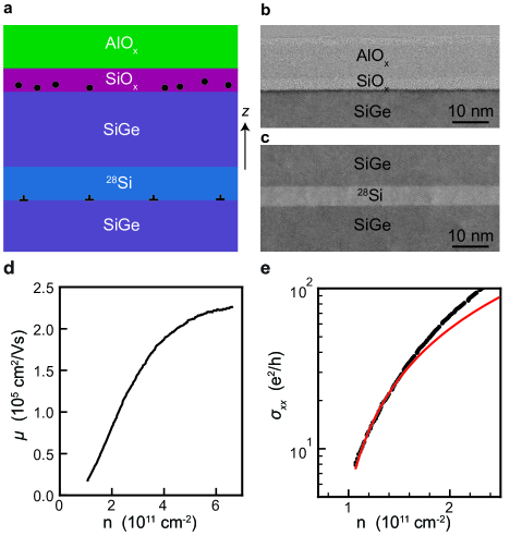
We consider three 28Si/SiGe heterostructures (A, B, C) to improve, in sequence, the semiconductor/dielectric interface (from A to B) and the crystalline quality of the quantum well (from B to C). Heterostructure A has an nm thick quantum well and is terminated with an epitaxial Si cap grown by dichlorosilane at 675 ∘C. This kind of heterostructure has already produced high performance spin-qubits[31, 6, 10]. Heterostructure B misses a final epitaxial Si cap but features an amorphous Si-rich layer obtained by exposing the SiGe barrier to dichlorosilane at 500 ∘C. Compared to A, heterostructure B supports a two-dimensional electron gas with enhanced and more uniform transport properties across a 100 mm wafer, owing to a more uniform SiOx layer with less scattering centers[32]. Finally, we introduce here heterostructure C, having the same amorphous Si-rich termination as in heterostructure B, but a thinner quantum well of nm (Supplementary Fig. 1). This is much thinner than the Matthews-Blakeslee critical thickness [33, 34], which is nm[35] for the relaxation of tensile Si on Si0.7Ge0.3 via the formation of misfit dislocation at the bottom interface of the quantum well.
Figures 1b, c show bright-field scanning transmission electron microscopy (BF-STEM) images from heterostructure C after fabrication of a Hall bar shaped heterostructure field effect transistors (H-FET). We observe a sharp SiGe/SiOx semiconductor/dielectric interface (Fig. 1b), characterised by a minor Ge pile up (dark line) in line with Ref. [32]. The nm thick quantum well (Fig. 1c) is uniform and has sharp interfaces to the nearby SiGe. No structural defects such as misfit dislocations are visible, suggesting they are, at most, scarce. By analysing Raman spectra (Supplementary Fig. 2), we estimate a tensile strain for the 28Si quantum wells in heterostrucure B and C of and , respectively, compared the expected strain of for the given stoichiometry of the heterostructures. These measurements point to significant strain relaxation in heterostructure B compared to C. In heterostructure B, the quantum wells approach the Matthews-Blakeslee critical thickness and therefore misfit dislocation segments are expected, in light of recent morphological characterisation of Si/SiGe heterostructures with similar quantum well thickness and SiGe chemical composition[36]. Due to the thinner quantum well, instead, heterostructure C adapts the epitaxial planes to the SiGe buffer much better than heterostructure B, meaning that misfit dislocations arising from strain-relaxation are, in principle, suppressed.
I.2 Electrical characterisation of H-FETs
We evaluate the scattering properties of the two-dimensional electron gases by wafer-scale electrical transport measured on Hall-bar shaped H-FETs operated in accumulation mode (Methods). For each heterostructure, multiple H-FETs over a wafer are measured in the same cool-down at a temperature of 1.7 K in refrigerators equipped with cryo-multiplexers[37]. Figures 1d, e show typical mobility-density and conductivity-density curves for heterostructure C, from which we extract the mobility measured at high density ( cm-2) and the percolation density ([38]. The mobility rises steeply at low density due to progressive screening of scattering from remote impurities and flattens at higher density ( cm-2), limited by scattering from impurities within or nearby the quantum well, for example uniform background charges, surface roughness, or crystalline defects such as threading or misfit dislocations[30, 39].
I.3 Charge noise measurements in quantum dots
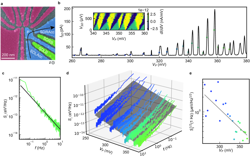
For charge noise measurements, we use devices comprising a double quantum dot and a charge sensor quantum dot nearby, illustrated in Fig. 2a. Using the same device design, two-qubit gates with fidelity above 99% were demonstrated[6], silicon quantum circuits were controlled by CMOS-based cryogenic electronics[31], and energy splittings in 28Si/SiGe heterostructures were studied with statistical significance[40].
Here, we electrostatically define a multi-electron quantum dot in the charge sensor by applying gate voltages to the accumulation gates SDRAcc and SDLAcc, the barriers SDLB and SDRB, and the plunger gate P. All other gates (red in Fig. 2a) are set to 0 V for measurements of heterostructure B and C, whereas they are positively biased in heterostructure A to facilitate charge accumulation in the sensor (Methods). Figure 2b shows typical Coulomb blockade oscillations of the source-drain current for a charge sensor from heterostructure C measured at a dilution refrigerator base temperature of 50 mK. We follow the same tune-up procedure (Methods) consistently for all devices and we measure charge noise at the flank of each Coulomb peak within the range defined by the first peak observable in transport and the last one before onset of a background channel (Supplementary Figs. 3,4). For example, in Figure 2b we consider Coulomb peaks within the range from 260 mV to 370 mV. The data collected in this systematic way is taken as a basis for comparison between the three different heterostructures in this study.
For each charge noise measurement at a given we acquire 60 s (heterostructure A) or 600 s (heterostructures B, C) long traces of and split them into 10 (heterostructure A) or 15 windows (heterostructures B, C). We obtain the current noise spectrum by averaging over the 10 (15) windows the discrete Fourier transform of the segments (Methods). We convert to a charge noise spectrum using lever arms from Coulomb diamond measurements and the slope of the Coulomb peaks (inset Fig. 2b, Methods, and Supplementary Fig.5). A representative charge noise spectrum measured at mV is shown in Fig. 2c. We observe an approximate trend at low frequency, pointing towards an ensemble of TLF with a broad range of activation energies affecting charge noise around the charge sensor [41, 42]. Figure 2e shows the charge noise at 1 Hz as a function of . The charge noise decreases, with a linear trend, with increasing , suggesting that, similar to scattering in 2D, screening by an increased electron density shields the electronically active region from noise arising from the heterostructure and the gate stack[43]. From this measurement we extract, for a given device, the minimum measured charge noise at 1 Hz () upon variation of in our experimental range. We use , as an informative metric to compare charge noise levels from device to device in a given heterostructure. For a given device, all charge noise spectra are plotted in 3D as a function of and (Fig. 2d). To quantify our observations, we fit the data to the plane with coefficient indicating the spectrum power law exponent and coefficient quantifying the change in noise spectrum with increasing plunger gate and, consequently, the susceptibility of charge noise to the increasing electron number in the sensor.
I.4 Distribution of transport properties and charge noise
We have introduced key metrics for 2D electrical transport (, ) and charge noise (, and ) from Hall bar and quantum dot measurements, respectively. In Figs. 3a–e we compare the distributions of all these metrics for the three heterostructures A, B, C. Each box-plot is obtained from the analysis of measurements in Figs. 1d,e, and Fig. 2d repeated on multiple H-FETs or quantum dots, on dies randomly selected from different locations across the 100 mm wafers (Methods). As reported earlier in Ref. [32], the improvement in both mean values and spread for and was associated with a reduction of remote impurities when replacing the epitaxial Si cap in heterostructure A with a Si-rich passivation layer in heterostructure B. Moving to heterostructure C, we measure a high mean mobility of cm2/Vs and a low mean percolation density of cm-2, representing an improvement by a factor 1.4 and 1.3, respectively (compared to heterostructure A). Most strikingly, the 99% confidence intervals of the mean for and are drastically reduced by a factor 9.8 and 4.8, respectively. We speculate that these improvements in heterostructure C are associated with the suppression of misfit dislocations at the quantum well/buffer interface, thereby reducing short range scattering and increasing uniformity on a wafer-scale. This interpretation is supported by the strain characterisation discussed above and by previous studies of mobility limiting mechanisms as a function of the quantum well thickness in strained Si/SiGe heterostructures[39].
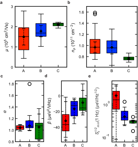
We now shift our attention to the results of charge noise measurements. First, the power law exponent (Fig. 3c) shows a mean value , however the 99% confidence interval and interquartile range increase when moving from heterostructure A to B and C. Next, we observe a decreasing trend for the absolute mean value of coefficient (Fig. 3d), meaning that the noise spectrum is less susceptible to changes in . Finally, we plot in Fig. 3e the distributions for , the minimum charge noise at 1 Hz upon varying . We find in heterostructure C an almost order of magnitude reduction in mean to . Furthermore, within the distribution of for heterostructure C, the minimum value of the measured charge noise as a function of and across quantum dots is . These charge noise values are on par or compare favourably to the best values reported previously at 1 Hz in gate defined quantum dots. In multi-electron quantum dots, charge noise of was reported for Si/SiGe[44], (average value, with a minimum of ) for Ge/SiGe[45], for Si/SiO2[46], and for InSb[47]. In single-electron quantum dots, charge noise of was reported for Si/SiGe[48] and for GaAs[49].
We understand the charge noise trends in Figs. 3c–e by relating them to the evolution of the disorder landscape moving from heterostructures A to B and C, as inferred by the electrical transport measurements in Figs. 3a,b. The narrow distribution of in heterostructure A points to charge noise from many TLFs possibly located at the low quality semiconductor/dielectric interface and above. Instead, the larger spread in in heterostructure B and C implies that deviations from behaviour become more frequent, possibly originating from a non-uniform distribution of TLF or from one low frequency TLF in the surrounding environment of the quantum dot that dominates the power spectrum in the measured interval. The electrical transport measurements support this interpretation: scattering from many remote impurities is dominant in heterostructure A, whereas with a better semiconductor/dielectric interface remote scattering has less impact in the transport metrics of heterostructures B and C.
The decreasing trend in is in line with the observation from electrical transport. As the impurity density decreases from heterostructure A to B and C, charge noise is less affected by an increasing , since screening of electrical noise through adding electrons to the charge sensor becomes less effective, possibly due to a smaller TLF-per-volume ratio. While we are not able to measure directly the electron number in the charge sensor, we deem unlikely the hypothesis that charge sensors in heterostructure A are operated with considerably fewer electrons than in heterostructure C. This is because all operation gate voltages in heterostructure A are consistently larger than in heterostructure C (Supplementary Fig. 4), due to the higher disorder.
Finally, the drastic reduction in mean value and spread of mirrors the evolution of mean value and spread of and . From heterostructure A to B, a reduction in scattering from remote impurities is likely to result in less charge noise from long-range TLFs. From heterostructure B to C, the larger strain, and consequently the reduction in the possible number of dislocations at the quantum well/buffer interface, further reduces the charge noise picked up by quantum dots. This explanation is based on earlier studies of charge noise in strained Si-MOSFETs[27, 28, 29], which showed a correlation between low-frequency noise spectral density and static device parameters. Dislocations at the bottom of the strained channel may act as scattering centers that degrade mobility and as traps for the capture and release of carriers, which causes noise similarly to traps at the dielectric interface.
I.5 Calculated dephasing time and infidelity
To emphasize the improvement of the electrical environment in the semiconductor host, we calculate the dephasing time of charge and spin qubits assuming these qubits experience the same fluctuations as our 28Si/SiGe quantum dots. The dephasing time of a qubit (in the quasistatic limit and far-off from a sweet spot) is given by [50]
| (1) |
with the Planck constant and the standard deviation
| (2) |
Importantly, both the charge noise amplitude and the noise exponent have a strong impact on the dephasing time while the low and high frequency cut-off, and , given by the duration of the experiment have a weaker impact. The prefactor translates shifts in chemical potential of the charge sensor into energy shifts of the qubit and depends on many parameters such as the type of qubit and the device itself. We find for a charge qubit [51] and for an uncoupled spin- qubit [44] (see Supplementary Information for a derivation of these numbers and the used frequency bandwidths).
Figure 4a shows the computed dephasing times of charge qubits (circle) and spin qubits (star) for all three heterostructures. The improvements in our material can be best seen by investigating of the charge qubit since it is directly affected by charge noise. Our theoretical extrapolation shows two orders of magnitude improvement in by switching from heterostructures A to heterostructures B and C 111One order is gained from the reduced charge noise amplitude and another order is gained through a more beneficial noise exponent .. Note, that the integration regimes differ for spin and charge qubits due to the different experimental setups and operation speeds [51, 44]. For potential spin qubits in heterostructure A the calculated shows an average = 8.4 5.6 µs. This distribution compares well with the distribution = 6.7 5.6 µs of experimental data from state-of-the-art semiconductor spin qubits in materials with similar stacks as in heterostructure A[6, 10]. Note that while such comparisons oversimplify actual semiconductor spin-qubit devices by reducing them to a single number, they fulfill two aims. They allow us to benchmark the computed performance of heterostructure A to past experiments and provide a prognosis on the qubit quality in novel material stacks. Heterostructures B and C, in this case, may support average dephasing times of = 24.3 12.5 µs and = 36.7 18 µs, respectively. The highest values = 70.1 µs hints towards a long spin qubit dephasing times previously only reported in Ref. [2].
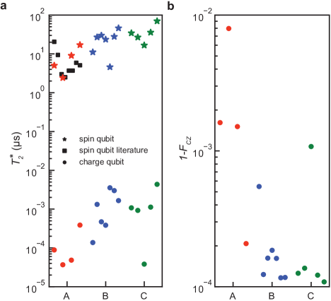
Figure 4b shows the simulated infidelity, a metric to measure the closeness to the ideal operation, of a universal cz-gate between two spin qubits following Ref. [6] and Section 5 in the Supplementary Information. Note, that the device used in Ref. [6] has the same architecture as our test devices. In the cz-gate simulation noise dominantly couples in via barrier voltage fluctuations which affects the interaction between the electron spins. Again, we assume the charge noise amplitude and exponents measured in our quantum dot experiments as input for the simulations. The simulations show an averaged average gate infidelity = 0.02 0.01 % which means on average a single error every 5000 runs. We also observe a saturation value close to which arises from single-qubit dephasing used in the simulations estimated from nuclear spin noise due to a 800 ppm concentration of the silicon isotope which has a non-zero nuclear spin [44].
II Discussion
In summary, we have measured electron transport and charge noise in 28Si/SiGe heterostructures where we improve the semiconductor/dielectric interface, by adopting an amorphous Si-rich passivation, and the structural quality of the quantum well, by reducing the quantum well thickness significantly below the Matthew-Blakeslee critical thickness for strain relaxation. We relate disorder in 2D to charge noise in quantum dots by following a statistical approach to measurements. A reduction of remote impurities and dislocations nearby the quantum well is connected with the key improvements in the scattering properties of the 2D electron gas, such as mobility and percolation density, and their uniformity across a 100 mm wafer. The trend observed from electron transport in 2D is compatible with the observations from measurements of charge noise in quantum dots. As remote impurities are reduced, charge noise becomes more sensitive to local fluctuators nearby the quantum well and less subject to screening by an increased number of electrons in the dot. Furthermore, with this materials optimization, we achieve a statistical improvement of nearly one order of magnitude in the charge noise supported by quantum dots. Using the charge noise distribution as input parameter and benchmarking against published spin-qubit data, we predict that our optimized semiconductor host could support long-lived and high-fidelity spin qubits. We envisage that further materials improvements in the structural quality of the quantum well, in addition to the commonly considered semiconductor/dielectric interface, may lead systematically to quantum dots with less noise and to better qubit performance.
References
- Vandersypen and Eriksson [2019] L. M. K. Vandersypen and M. A. Eriksson, Physics Today 72, 38 (2019).
- Veldhorst et al. [2015] M. Veldhorst, C. H. Yang, J. C. C. Hwang, W. Huang, J. P. Dehollain, J. T. Muhonen, S. Simmons, A. Laucht, F. E. Hudson, K. M. Itoh, A. Morello, and A. S. Dzurak, Nature 526, 410 (2015).
- Stano and Loss [2022] P. Stano and D. Loss, Nature Reviews Physics (2022), 10.1038/s42254-022-00484-w.
- Zwerver et al. [2022] A. M. J. Zwerver, T. Krähenmann, T. F. Watson, L. Lampert, H. C. George, R. Pillarisetty, S. A. Bojarski, P. Amin, S. V. Amitonov, J. M. Boter, R. Caudillo, D. Correas-Serrano, J. P. Dehollain, G. Droulers, E. M. Henry, R. Kotlyar, M. Lodari, F. Lüthi, D. J. Michalak, B. K. Mueller, S. Neyens, J. Roberts, N. Samkharadze, G. Zheng, O. K. Zietz, G. Scappucci, M. Veldhorst, L. M. K. Vandersypen, and J. S. Clarke, Nature Electronics 5, 184 (2022).
- Watson et al. [2018] T. F. Watson, S. G. J. Philips, E. Kawakami, D. R. Ward, P. Scarlino, M. Veldhorst, D. E. Savage, M. G. Lagally, M. Friesen, S. N. Coppersmith, M. A. Eriksson, and L. M. K. Vandersypen, Nature 555, 633 (2018).
- Xue et al. [2022] X. Xue, M. Russ, N. Samkharadze, B. Undseth, A. Sammak, G. Scappucci, and L. M. K. Vandersypen, Nature 601, 343 (2022).
- Noiri et al. [2022a] A. Noiri, K. Takeda, T. Nakajima, T. Kobayashi, A. Sammak, G. Scappucci, and S. Tarucha, Nature 601, 338 (2022a).
- Ma̧dzik et al. [2022] M. T. Ma̧dzik, S. Asaad, A. Youssry, B. Joecker, K. M. Rudinger, E. Nielsen, K. C. Young, T. J. Proctor, A. D. Baczewski, A. Laucht, V. Schmitt, F. E. Hudson, K. M. Itoh, A. M. Jakob, B. C. Johnson, D. N. Jamieson, A. S. Dzurak, C. Ferrie, R. Blume-Kohout, and A. Morello, Nature 601, 348 (2022).
- Mills et al. [2022] A. R. Mills, C. R. Guinn, M. J. Gullans, A. J. Sigillito, M. M. Feldman, E. Nielsen, and J. R. Petta, Science Advances 8, eabn5130 (2022).
- Philips et al. [2022] S. G. J. Philips, M. T. Ma̧dzik, S. V. Amitonov, S. L. de Snoo, M. Russ, N. Kalhor, C. Volk, W. I. L. Lawrie, D. Brousse, L. Tryputen, B. P. Wuetz, A. Sammak, M. Veldhorst, G. Scappucci, and L. M. K. Vandersypen, Preprint at http://arxiv.org/abs/2202.09252 (2022).
- Samkharadze et al. [2018] N. Samkharadze, G. Zheng, N. Kalhor, D. Brousse, A. Sammak, U. C. Mendes, A. Blais, G. Scappucci, and L. M. K. Vandersypen, Science 359, 1123 (2018).
- Zajac et al. [2018] D. M. Zajac, A. J. Sigillito, M. Russ, F. Borjans, J. M. Taylor, G. Burkard, and J. R. Petta, Science 359, 439 (2018).
- Borjans et al. [2020] F. Borjans, X. G. Croot, X. Mi, M. J. Gullans, and J. R. Petta, Nature 577, 195 (2020).
- Harvey-Collard et al. [2022] P. Harvey-Collard, J. Dijkema, G. Zheng, A. Sammak, G. Scappucci, and L. M. K. Vandersypen, Physical Review X 12, 021026 (2022).
- Yoneda et al. [2021] J. Yoneda, W. Huang, M. Feng, C. H. Yang, K. W. Chan, T. Tanttu, W. Gilbert, R. C. C. Leon, F. E. Hudson, K. M. Itoh, A. Morello, S. D. Bartlett, A. Laucht, A. Saraiva, and A. S. Dzurak, Nature Communications 12, 4114 (2021).
- Noiri et al. [2022b] A. Noiri, K. Takeda, T. Nakajima, T. Kobayashi, A. Sammak, G. Scappucci, and S. Tarucha, Preprint at http://arXiv:2202.01357 (2022b).
- Vandersypen et al. [2017] L. M. K. Vandersypen, H. Bluhm, J. S. Clarke, A. S. Dzurak, R. Ishihara, A. Morello, D. J. Reilly, L. R. Schreiber, and M. Veldhorst, npj Quantum Information 3, 1 (2017).
- Yoneda et al. [2018] J. Yoneda, K. Takeda, T. Otsuka, T. Nakajima, M. R. Delbecq, G. Allison, T. Honda, T. Kodera, S. Oda, Y. Hoshi, N. Usami, K. M. Itoh, and S. Tarucha, Nature Nanotechnology 13, 102 (2018).
- Paladino et al. [2014] E. Paladino, Y. M. Galperin, G. Falci, and B. L. Altshuler, Reviews of Modern Physics 86, 361 (2014).
- Connors et al. [2019] E. J. Connors, J. J. Nelson, H. Qiao, L. F. Edge, and J. M. Nichol, Physical Review B 100, 165305 (2019).
- Connors et al. [2022] E. J. Connors, J. Nelson, L. F. Edge, and J. M. Nichol, Nature Communications 13, 940 (2022).
- Culcer et al. [2009] D. Culcer, X. Hu, and S. Das Sarma, Applied Physics Letters 95, 073102 (2009).
- Dekker et al. [1991] C. Dekker, A. J. Scholten, F. Liefrink, R. Eppenga, H. van Houten, and C. T. Foxon, Physical Review Letters 66, 2148 (1991).
- Sakamoto et al. [1995] T. Sakamoto, Y. Nakamura, and K. Nakamura, Applied Physics Letters 67, 2220 (1995).
- Liefrink et al. [1994] F. Liefrink, J. I. Dijkhuis, and H. v. Houten, Semiconductor Science and Technology 9, 2178 (1994).
- Ramon and Hu [2010] G. Ramon and X. Hu, Physical Review B 81, 045304 (2010).
- Hua et al. [2005] W.-C. Hua, M. Lee, P. Chen, M.-J. Tsai, and C. Liu, IEEE Electron Device Letters 26, 667 (2005).
- Lee et al. [2003] M. Lee, P. Chen, W.-C. Hua, C.-Y. Yu, Y. Tseng, S. Maikap, Y. Hsua, C. Liu, S. Lu, W.-Y. Hsieh, and M.-J. Tsai, in IEEE International Electron Devices Meeting 2003 (2003) pp. 3.6.1–3.6.4.
- Simoen et al. [2006] E. Simoen, G. Eneman, P. Verheyen, R. Loo, Kristin De Meyer, and C. Claeys, IEEE Transactions on Electron Devices 53, 1039 (2006).
- Monroe [1993] D. Monroe, Journal of Vacuum Science & Technology B: Microelectronics and Nanometer Structures 11, 1731 (1993).
- Xue et al. [2021] X. Xue, B. Patra, J. P. G. van Dijk, N. Samkharadze, S. Subramanian, A. Corna, B. P. Wuetz, C. Jeon, F. Sheikh, E. Juarez-Hernandez, B. P. Esparza, H. Rampurawala, B. Carlton, S. Ravikumar, C. Nieva, S. Kim, H.-J. Lee, A. Sammak, G. Scappucci, M. Veldhorst, F. Sebastiano, M. Babaie, S. Pellerano, E. Charbon, and L. M. K. Vandersypen, Nature 593, 205 (2021).
- Degli Esposti et al. [2022] D. Degli Esposti, B. Paquelet Wuetz, V. Fezzi, M. Lodari, A. Sammak, and G. Scappucci, Applied Physics Letters 120, 184003 (2022).
- Matthews and Blakeslee [1974] J. W. Matthews and A. E. Blakeslee, Journal of Crystal growth 27, 118 (1974).
- People and Bean [1985] R. People and J. C. Bean, Applied Physics Letters 47, 322 (1985).
- Ismail [1996] K. Ismail, Journal of Vacuum Science & Technology B: Microelectronics and Nanometer Structures 14, 2776 (1996).
- Liu et al. [2022] Y. Liu, K.-P. Gradwohl, C.-H. Lu, T. Remmele, Y. Yamamoto, M. H. Zoellner, T. Schroeder, T. Boeck, H. Amari, C. Richter, and M. Albrecht, Journal of Applied Physics 132, 085302 (2022).
- Paquelet Wuetz et al. [2020] B. Paquelet Wuetz, P. L. Bavdaz, L. A. Yeoh, R. Schouten, H. van der Does, M. Tiggelman, D. Sabbagh, A. Sammak, C. G. Almudever, F. Sebastiano, J. S. Clarke, M. Veldhorst, and G. Scappucci, npj Quantum Information 6, 43 (2020).
- Tracy et al. [2009] L. A. Tracy, E. H. Hwang, K. Eng, G. A. Ten Eyck, E. P. Nordberg, K. Childs, M. S. Carroll, M. P. Lilly, and S. Das Sarma, Physical Review B 79, 235307 (2009).
- Ismail et al. [1994] K. Ismail, F. K. LeGoues, K. L. Saenger, M. Arafa, J. O. Chu, P. M. Mooney, and B. S. Meyerson, Physical Review Letters 73, 3447 (1994).
- Paquelet Wuetz et al. [2021] B. Paquelet Wuetz, M. P. Losert, S. Koelling, L. E. A. Stehouwer, A.-M. J. Zwerver, S. G. J. Philips, M. T. Madzik, X. Xue, G. Zheng, M. Lodari, S. V. Amitonov, N. Samkharadze, A. Sammak, L. M. K. Vandersypen, R. Rahman, S. N. Coppersmith, O. Moutanabbir, M. Friesen, and G. Scappucci, Preprint at http://arxiv.org/abs/2112.09606 (2021).
- Kogan [1996] S. Kogan, Electronic Noise and Fluctuations in Solids (Cambridge University Press, 1996).
- Ahn et al. [2021] S. Ahn, S. D. Sarma, and J. P. Kestner, Physical Review B 103, L041304 (2021).
- Thorgrimsson et al. [2017] B. Thorgrimsson, D. Kim, Y.-C. Yang, L. W. Smith, C. B. Simmons, D. R. Ward, R. H. Foote, J. Corrigan, D. E. Savage, M. G. Lagally, M. Friesen, S. N. Coppersmith, and M. A. Eriksson, npj Quantum Information 3, 32 (2017).
- Struck et al. [2020] T. Struck, A. Hollmann, F. Schauer, O. Fedorets, A. Schmidbauer, K. Sawano, H. Riemann, N. V. Abrosimov, Łukasz Cywiński, D. Bougeard, and L. R. Schreiber, npj Quantum Information 6, 40 (2020).
- Lodari et al. [2021] M. Lodari, N. W. Hendrickx, W. I. L. Lawrie, T.-K. Hsiao, L. M. K. Vandersypen, A. Sammak, M. Veldhorst, and G. Scappucci, Materials for Quantum Technology 1, 11002 (2021).
- Freeman et al. [2016] B. M. Freeman, J. S. Schoenfield, and H. Jiang, Applied Physics Letters 108, 253108 (2016).
- Jekat et al. [2020] F. Jekat, B. Pestka, D. Car, S. Gazibegović, K. Flöhr, S. Heedt, J. Schubert, M. Liebmann, E. P. A. M. Bakkers, T. Schäpers, and M. Morgenstern, Applied Physics Letters 116, 253101 (2020).
- Mi et al. [2018] X. Mi, S. Kohler, and J. R. Petta, Physical Review B 98, 161404 (2018).
- Basset et al. [2014] J. Basset, A. Stockklauser, D.-D. Jarausch, T. Frey, C. Reichl, W. Wegscheider, A. Wallraff, K. Ensslin, and T. Ihn, Applied Physics Letters 105, 063105 (2014).
- Ithier et al. [2005] G. Ithier, E. Collin, P. Joyez, P. J. Meeson, D. Vion, D. Esteve, F. Chiarello, A. Shnirman, Y. Makhlin, J. Schriefl, and G. Schön, Physical Review B 72, 134519 (2005).
- MacQuarrie et al. [2020] E. R. MacQuarrie, S. F. Neyens, J. P. Dodson, J. Corrigan, B. Thorgrimsson, N. Holman, M. Palma, L. F. Edge, M. Friesen, S. N. Coppersmith, and M. A. Eriksson, npj Quantum Information 6, 81 (2020).
- Note [1] One order is gained from the reduced charge noise amplitude and another order is gained through a more beneficial noise exponent .
- Sabbagh et al. [2019] D. Sabbagh, N. Thomas, J. Torres, R. Pillarisetty, P. Amin, H. George, K. Singh, A. Budrevich, M. Robinson, D. Merrill, L. Ross, J. Roberts, L. Lampert, L. Massa, S. Amitonov, J. Boter, G. Droulers, H. Eenink, M. van Hezel, D. Donelson, M. Veldhorst, L. Vandersypen, J. Clarke, and G. Scappucci, Physical Review Applied 12, 014013 (2019).
III Methods
Si/SiGe heterostructure growth. The 28Si/SiGe heterostructures are grown on a 100-mm n-type Si(001) substrate using an Epsilon 2000 (ASMI) reduced pressure chemical vapor deposition reactor. The reactor is equipped with a 28SiH4 gas cylinder (1% dilution in H2) for the growth of isotopically enriched 28Si. The 28SiH4 gas was obtained by reducing 28SiF4 with a residual 29Si concentration of 0.08%[53]. Starting from the Si substrate, the layer sequence of all heterostructures comprises a 3 µm step-graded Si(1-x)Gex layer with a final Ge concentration of achieved in four grading steps (, 0.14, 0.21, and 0.3), followed by a 2.4 µm Si0.7Ge0.3 strain-relaxed buffer. The heterostructures differ for the active layers on top of the strain-relaxed buffer. Heterostructure A has a 9 nm tensile strained 28Si quantum well, a 30 nm Si0.7Ge0.3 barrier, and a sacrificial 1 nm epitaxial Si cap. Heterostructure B has an 9 nm tensile strained 28Si quantum well, a 30 nm Si0.7Ge0.3 barrier, and a sacrificial passivated Si cap grown at 500 ∘C. Heterostructure C has a 5 nm tensile strained 28Si quantum well, a 30 nm Si0.7Ge0.3 barrier, and a sacrificial passivated Si cap grown at 500 ∘C. A typical secondary ions mass spectrometry of our heterostructures is reported in Fig. S13 of [40] and the Ge concentration in the SiGe layers is confirmed by quantitative electron energy loss spectroscopy (EELS).
Device fabrication. The fabrication process for Hall-bar shaped heterostructure field effect transistors (H-FETs) involves: reactive ion etching of mesa-trench to isolate the two-dimensional electron gas; P-ion implantation and activation by rapid thermal annealing at 700 ∘C; atomic layer deposition of a 10-nm-thick Al2O3 gate oxide; deposition of thick dielectric pads to protect gate oxide during subsequent wire bonding step; sputtering of Al gate; electron beam evaporation of Ti:Pt to create ohmic contacts to the two-dimensional electron gas via doped areas. All patterning is done by optical lithography. Double quantum dot devices are fabricated on wafer coupons from the same H-FET fabrication run and share the process steps listed above. Double-quantum dot devices feature a single layer gate metallization and further require electron beam lithography, evaporation of Al (27 nm) or Ti:Pd (3:27 nm) thin film metal gate, lift-off, and the global top-gate layer.
Electrical characterization of H-FETs. Hall-bar H-FETs measurements are performed in an attoDRY2100 variable temperature insert refrigerator at a base temperature of 1.7 K[32]. We apply a source-drain bias of 100 µV and measure the source-drain current , the longitudinal voltage , and the transverse Hall voltage as function of the top gate voltage and the external perpendicular magnetic field . From here we calculate the longitudinal resistivity and transverse Hall resistivity . The Hall electron density is obtained from the linear relationship at low magnetic fields. The carrier mobility is extracted from the relationship , where is the electron charge. The percolation density is extracted by fitting the longitudinal conductivity to the relation . Here is obtained via tensor inversion of at . The box plots in Figs. 3a,b for heterostructure A (red) and B (blue) expand previously published data in Figs. 2f,e of Ref. [32] by considering measurements of 4 additional H-FETs for heterostructure A (20 H-FETs in total) and of 2 additional H-FETs for heterostructure B (16 H-FETs in total).
Electrical characterization of quantum dots. Measurements of the multi-electron quantum dots defined in the charge sensor are performed in a Leiden cryogenic dilution refrigerator with a mixing chamber base temperature mK[40]. The devices are tuned systematically with the following procedure. We sweep all gate voltages (, , , , and ) from 0 V towards more positive bias, until a source-drain current of 1 nA is measured, indicating that a conductive channel has formed in the device. We then reduce the barrier voltages to find the pinch-off voltages for each barrier. Subsequently, we measure as a function of and and from this 2D map we find a set of gate voltage parameters so that Coulomb blockade peaks are visible. We then fix the barrier voltages and sweep VP to count how many clearly defined Coulomb peaks are observed before onset of a background current. The quantum dot is tuned to show at least 9 Coulomb peaks, so that noise spectra may be fitted as in Fig. 2d with meaningful error bars. If we see less than 9 Coulomb peaks we readjust the accumulation gate voltages , and , and repeat the 2D scan of against . In one case (device 2 of heterostructure A), we tuned device to show past 5 Coulomb peaks and still performed the fit of the charge noise spectra similar to the one shown in Fig. 2d. Further details on the extraction of the lever arms and operation gate voltages of the devices are provided in Supplementary Figs 4,5. We estimate an electron temperature of 190 mK by fitting Coulomb blockade peaks (see Supplementary Fig. 2 in Ref. [32]) measured on quantum dot devices.
For heterostructure A we apply a source drain bias of 100 µV (1 device) or 150 µV (3 devices) across the quantum dot, finite gate voltages across the operation gates of the dot, and finite gate voltages across the screening gates. We measure the current and the current noise spectrum on the left side of the Coulomb peak where is largest. We use a sampling rate of 1 kHz for 1 minute using a Keithley DMM6500 multimeter. The spectra are then divided into 10 segments of equal length and we use a Fourier transform to convert from time-domain to frequency-domain for a frequency range of 167 mHz-500 Hz. We set the upper limit of the frequency spectra at 10 Hz, to avoid influences from a broad peak at around 150 Hz coming from the setup (Supplementary Fig. 3). A peak in the power spectral density at 9 Hz is removed from the analysis since it is an artifact of the pre-amplifier. To convert the current noise spectrum to a charge noise spectrum we use the formula
| (3) |
where is the lever arm and is the slope of Coulomb peak around the center of the Coulomb peak.
For heterostructures B and C we apply a source drain bias of 150 µV across the quantum dot, finite gate voltages across the operation gates of the quantum dot, and we apply 0 V to all other gates. We measure the current and the current noise spectrum on the left side of the Coulomb peak where is largest. We use a sampling rate of 1 kHz for 10 minutes using a Keithley DMM6500 multimeter. The spectra are then divided into 15 segments of equal length and we use a Fourier transform to convert from time-domain to frequency-domain for a frequency range of 25 mHz-500 Hz. We set the upper limit of the frequency spectra at 10 Hz, to avoid influences from a broad peak at around 150 Hz coming from the setup. We use Eq. 3 to convert the current noise spectrum to a charge noise spectrum.
(Scanning) Transmission Electron Microscopy. For structural characterization with (S)TEM, we prepared cross-sections of the quantum well heterostructures by using a Focused Ion Beam (Helios 600 dual beam microscope). HR-TEM micrographs were acquired in a TECNAI F20 microscope operated at 200 kV. Atomically resolved HAADF STEM data was acquired in a probe corrected TITAN microscope operated at 300 kV. EELS mapping was carried out in a TECNAI F20 microscope operated at 200 kV with approximately 2 eV energy resolution and 1 eV energy dispersion. Principal Component Analysis (PCA) was applied to the spectrum images to enhance S/N ratio.
IV Data availability
All data included in this work are available from the 4TU.ResearchData international data repository at https://doi.org/10.4121/20418579
V Acknowledgements
We acknowledge helpful discussions with G. Isella, D. Paul, M. Mehmandoost, the Scappucci group and the Vandersypen group.
This research was supported by the European Union’s Horizon 2020 research and innovation programme under the Grant Agreement No. 951852 (QLSI project) and in part by the Army Research Office (Grant No. W911NF-17-1-0274). The views and conclusions contained in this document are those of the authors and should not be interpreted as representing the official policies, either expressed or implied, of the Army Research Office (ARO), or the U.S. Government. The U.S. Government is authorized to reproduce and distribute reprints for Government purposes notwithstanding any copyright notation herein. M.R. acknowledges support from the Netherlands Organization of Scientific Research (NWO) under Veni grant VI.Veni.212.223. ICN2 acknowledges funding from Generalitat de Catalunya 2017 SGR 327. ICN2 is supported by the Severo Ochoa program from Spanish MINECO (Grant No. SEV-2017-0706) and is funded by the CERCA Programme / Generalitat de Catalunya and ERDF funds from EU. Part of the present work has been performed in the framework of Universitat Autònoma de Barcelona Materials Science PhD program. Authors acknowledge the use of instrumentation as well as the technical advice provided by the National Facility ELECMI ICTS, node ”Laboratorio de Microscopias Avanzadas” at University of Zaragoza. M.B. acknowledges support from SUR Generalitat de Catalunya and the EU Social Fund; project ref. 2020 FI 00103. We acknowledge support from CSIC Interdisciplinary Thematic Platform (PTI+) on Quantum Technologies (PTI-QTEP+).
VI Authors contributions
A.S. grew and designed the 28Si/SiGe heterostructures with B.P.W. and G.S.. M.R. developed the theory. A.S. and D.D.E. fabricated heterostructure field effect transistors measured by B.P.W. and D.D.E.. M.B and J.A. performed TEM characterisation. S.A and D.D.E. fabricated quantum dot devices. B.P.W. and D.D.E. measured the quantum dot devices with contributions from A.M.J.Z.. G.S. conceived and supervised the project. B.P.W, M.R, and G.S. wrote the manuscript with input from all authors.
VII Competing Interests
The authors declare no competing interests.
VIII Additional information
Supplementary Information Supplementary Figs. 1–5 and Discussion.
Correspondence and request for materials should be addressed to G.S.