Shared control of a 16 semiconductor quantum dot crossbar array
Abstract
The efficient control of a large number of qubits is one of most challenging aspects for practical quantum computing. Current approaches in solid-state quantum technology are based on brute-force methods, where each and every qubit requires at least one unique control line, an approach that will become unsustainable when scaling to the required millions of qubits. Here, inspired by random access architectures in classical electronics, we introduce the shared control of semiconductor quantum dots to efficiently operate a two-dimensional crossbar array in planar germanium. We tune the entire array, comprising 16 quantum dots, to the few-hole regime and, to isolate an unpaired spin per dot, we confine an odd number of holes in each site. Moving forward, we establish a method for the selective control of the quantum dots interdot coupling and achieve a tunnel coupling tunability over more than 10 GHz. The operation of a quantum electronic device with fewer control terminals than tunable experimental parameters represents a compelling step forward in the construction of scalable quantum technology.
Fault-tolerant quantum computers will require millions of interacting qubits [1, 2, 3].
Scaling to such extreme numbers imposes stringent conditions on all the hardware and software components, including their integration [4].
In semiconductor technology, decades of advancements have led to the integration of billions of transistor components on a single chip.
A key enabler has been the ability to control such a large number of components with only a few hundred to a few thousand control lines [5, 6].
In quantum technology, such a game-changing strategy has yet to be embraced owing to the fact that qubits are not sufficiently similar to each other.
Nowadays, leading efforts in solid state, such as superconducting and semiconducting qubits, all require that each and every qubit component is connected to at least one unique control line [7].
Clearly, this brute-force approach is not sustainable for attaining practical quantum computation.
The development of spin qubits in semiconductor quantum dots has strongly been inspired by classical semiconductor technology [8, 9, 10].
Advanced semiconductor qubit systems are based on CMOS compatible materials and even foundry manufactured qubits have been realised [11, 12].
In addition, it is anticipated that the small qubit footprint and compatibility with (cryo-)CMOS electronics will open up avenues to build integrated quantum circuits [13, 14].
To enable the efficient control of larger qubit architectures with a sustainable number of control lines, proposals of architectures inspired by classical random access systems have been put forward [15, 16].
However, their practical realisation has been so far prevented by device quality and material uniformity.
Here, we take the first step toward the sustainable control of large quantum processors by operating semiconductor quantum dots in a crossbar architecture. This strategy enables the manipulation of the most extensive semiconductor quantum device with only a few shared-control terminals. This is accomplished by exploiting the high quality and uniformity of strained germanium quantum wells [17], by introducing an elegant gate layout based on diagonal plunger lines and double barrier gates, and by establishing a method that directly maps the transitions lines of charge stability diagrams to the associated quantum dots in the grid. We operate a two-dimensional 16 quantum dot system and demonstrate the tune-up of the full device to the few-hole regime. In this configuration, we also prove the ability to prepare all the quantum dots in the odd charge occupation, as a key step for the confinement of an unpaired spin in each site [18, 19]. We then introduce a random access method for addressing the interdot tunnel coupling and find a remarkable agreement in the response of two vertically- and horizontally-coupled quantum dot pairs. We also discuss some critical challenges to efficiently operating future large quantum circuits.
I A two-dimensional quantum dot crossbar array
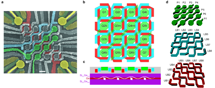
Our shared-terminals control approach for a two-dimensional quantum dot array with dots Q1, Q2t,…Q7 is based on a multi-layer gate architecture (Figs. 1a-d).
We use two barrier layers (with gates UB and LB with ) to control the interdot tunnel couplings, and exploit a layer of plunger lines (P with ) to vary the on-site energies (Fig. 1d).
In contrast to brute-force implementations, a single plunger gate is here employed to control up to four quantum dots, and an individual barrier up to six nearest-neighbours interactions.
In analogy with classical integrated circuits, this strategy enables to manage a number of experimental parameters (i.e., dot energies and interdot couplings) with a sub-linear number of control terminals, an approach that may overcome, among other aspects, the wiring interconnect bottleneck of large-scale spin qubit arrays (Suppl. Fig. 1) [6, 7].
To monitor the quantum dot array, we make use of charge sensing techniques [18].
Four single-hole transistors at the corners of the array (named after their cardinal positions: NW as north-west, NE as north-east, SW as south-west and SE as south-east) act as charge sensors as well as holes reservoirs for the array.
The simultaneous read-out of their electrical response in combination with fast rastering pulse schemes enables us to continuously measure two-dimensional charge stability diagrams in real time (Methods) [20, 21].
To bring the device in the 16 quantum dots configuration, we identify an alternative strategy to the tune-up methods established for individually-controlled quantum dot devices [22].
We begin by lowering all gate voltages to starting values based on previous experiments (Methods).
We set up the four independent charge sensors (Suppl. Fig. 2) and start defining a set of virtual gates as linear combinations of real gates [23, 24, 22].
Throughout our work, we refer to vP1,…, vP7, vUB1,…, vUB8, vLB1,…, vLB8 as the virtual gates associated to the actual gates P1,…, P7, UB1,…, UB8, LB1,…, LB8 (Methods and Suppl. Fig. 3).
By further adjusting the respective virtual plunger and barrier voltages, we then accumulate the first holes in the quantum dots at the four corners of the array.
Once clear charge addition lines are detected in the charge stability diagrams, we proceed with the tune-up of the adjacent dots and finish with the quantum dots furthest to the sensor.
Owing to the homogeneity of our heterostructure [25] and the symmetry of our gate layout, the accumulation of the first few holes in quantum dots controlled by the same plungers occurs at similar gate voltages.
Rather, challenges in the tuning up the array that we encounter are mainly due to elements outside the array.
In fact, we observe that small variations of the gate voltages impact the electrostatics of the dense gate fanout area, which in turn affects the charge sensors and the readout quality.
Furthermore, specific gate settings cause unintentional quantum dots under the gate fanout, which restrict the operational window.
Altogether, these issues are a challenge for the implementation of automated tuning methods [26].
We envision that the integration of a lower layer of “screening” gates or the implementation of the gate fanout in the third dimension [27] can mitigate this issue (Suppl. Note 4).
II From multi-dot charge stability diagrams to quantum dots identification
Moving forward, a direct result of our control approach is the fact that, upon sweeping the voltage of a plunger gate controlling quantum dots, up to sets of charge transitions can be observed, each associated with (un)loading an additional hole in one of the quantum dots.
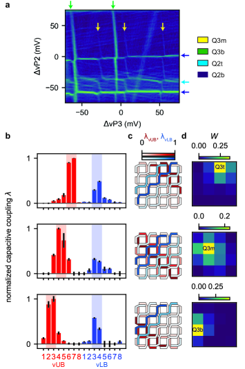
For the case of the two shared virtual plungers vP2 and vP3, this results in the charge stability diagram shown in Fig. 2a where a number of vertical and horizontal charge addition lines marking well separate charge states are visible.
However, because of our control approach, a priori it is unknown to which of the Q3 (Q2) quantum dots these vertical (horizontal) lines are associated.
Here, we solve this problem by establishing a statistical method that maps such transition lines to the respective quantum dot.
In our protocol, we first evaluate the shift of the charge transition lines induced by a voltage variation of each barrier gate to estimate the (normalized) capacitive coupling between each barrier gate and the associated quantum dot (Figs. 2b, c and Methods).
Because the two barrier layers form a grid of lines and columns crossing the device, we then use their capacitive couplings to infer the spatial location of the quantum dot in the array.
For this purpose, we consider the normalised capacitive couplings of the two orthogonal barrier sets, and , as two independent probability distributions.
We then use and to calculate the combined probability on each of the 16 sites (Fig. 2d, Methods).
Finally, our protocol ends assigning the site with the maximum probability to the quantum dot loaded via the specific charge addition lines.
In practice, quantifies how much an electric field generated on each site is perceived by a hole in a specific quantum dot site.
Hence, a low (high) value identifies a location that is weakly (strongly) coupled to the analysed quantum dot.
In Figs. 2b-d, we show how this routine is effective for distinguishing and characterising the three Q3 quantum dots, whereas similar results are obtained also for the remaining dots in the grid (Suppl. Figs. 4 and 5).
The demonstrated ability of labelling multi-quantum dot charge stability diagrams makes this method an important tool in the tune-up of large quantum dot devices.
We note that we can obtain further confirmation of our identification by also considering other aspects, such as the different sensitivity of the charge sensors to the same set of charge addition lines (e.g. compare Suppl. Figs. 6e, j, c).
III Quantum dot occupancies
Whilst useful in reducing drastically the number of control terminals, a crossbar approach is effective for spin-based quantum computing if it enables to isolate a single or an unpaired spin in the individual quantum dots [8, 16].
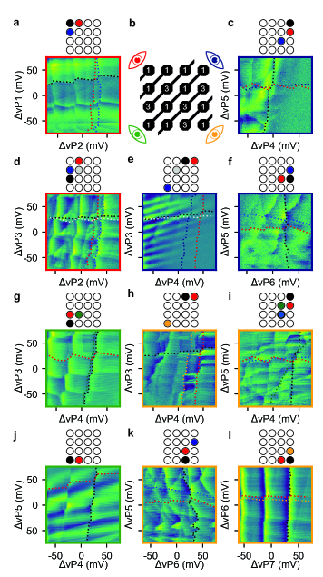
Here, by harnessing the low disorder of the heterostructure and the symmetry of our design, we demonstrate the tune-up of the array to an odd charge occupancy configuration with 11 quantum dots filled with one hole, and five quantum dots filled with three holes (Fig. 3b).
Figs. 3a,c-l present a set of charge stability diagrams where the transition lines of each quantum dots are shown and labelled at least once.
Importantly, at the centre of the panels (i.e., vP = 0, with ), each quantum dot is filled with an odd number of holes, hence with an unpaired hole spin (Methods).
We note that holes in quantum dots that are located in the core of the array are loaded/unloaded by means of cotunneling processes via the outer dots [28].
When such reservoir-dot tunnelling timescale becomes long and approaches the timescale of our measurement scan ( s), the quantum dots transition lines become weakly visible in the charge stability diagrams and appear distorted due to latching effects, explaining some of the features observed in Figs. 3h, i, k. [29, 30].
Additional reservoirs within the array may therefore simply the tune-up, though for quantum operation is it not critical to have each and every dot strongly coupled to a reservoir [6, 10].
IV Interdot couplings control
The ability to selectively tune the interdot coupling in a quantum dot architecture is crucial for generating exchange-based entanglement between semiconductor qubits [8].
Here, inspired by the word and bitlines approach as in dynamic random-access memories [13, 16], we exploit the double barrier design to spatially define and activate unique points in the grid structure.
Conceptually, each two-barrier intersection point can be set by the respective voltages in the four configurations: (ON, ON), (ON, OFF), (OFF, ON), (OFF, OFF).
For selective two-qubit operations in qubit arrays, the voltage set points should be calibrated such that only when both barriers are in the ON-state a two-qubit interaction is activated, leaving all the other pairs non-interacting (Suppl. Fig. 7).
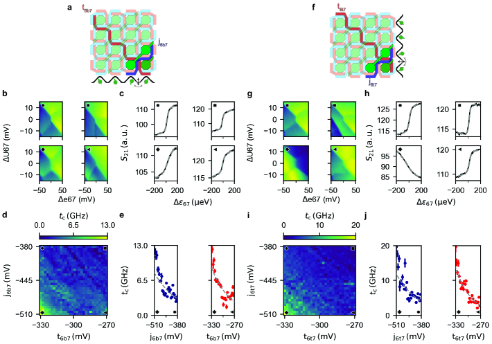
Here, we implement a proof-of-principle of this method by demonstrating the two-barrier control of the interdot tunnel coupling.
To this end, we investigate the tunnel coupling variations of the horizontal Q6b-Q7 and vertical Q6t-Q7 quantum dot pairs as a function of the two intersecting barriers.
Starting from the respective UB4 and LB7 gates, we define the virtual barriers and (Methods), which separate the quantum dots Q6b and Q7, while keeping their detuning (e67) and on-site (U67) voltages constant at the (3,1)-(2,2) Q6b-Q7 interdot transition (Fig. 4a). After obtaining the detuning lever arm to convert the detuning voltage into an energy scale (e67), we evaluate the strength of the interdot couplings by analysing the charge polarisation lines along the detuning axis at U67 = 0 (Figs. 4b, c) [31].
By performing this measurement systematically, we demonstrate that the tunnel coupling can be controlled effectively by both barriers (Figs. 4d,e).
At values of mV, the coupling is virtually OFF, but our method is inherently not accurate for GHz, because the thermal energy dominates the broadening of the polarisation line [31, 29]. In contrast, upon activating both barriers at mV, the tunnel coupling is turned on following approximately an exponential trend (Methods). Within the displayed voltage range, we can tune it well above 10 GHz, much higher than in the configuration in which only one barrier is activated.
We perform the same experiment on the dots pair Q6t-Q7 by defining the virtual barriers and based on the gates UB5 and LB7, respectively (Fig. 4f and Methods).
Using the same barrier voltages window as for Q6b-Q7, we find that the coupling tunability of the pair Q6t-Q7 is comparable to the previous pair, with a virtually OFF state ( 3 GHz) at mV, and with a ON state reaching 20 GHz at mV (Figs. 4g-j).
These results are corroborated by the two-barrier tunability of the interdot capacitive coupling for both double-dot systems (Suppl. Fig. 8) and by the tunability of another dot pair (Suppl. Fig. 9).
We envision that for rapid qubits exchange operations at the charge symmetry point, the required barrier voltage window might be different from our measurable window via polarisation lines.
Specifically, for state-of-the-art values of ON (OFF) exchange interaction of 50 MHz (10 KHz) and a typical charging energy of 1 mV, the required tunnel coupling is (0.02) GHz, which can be better calibrated via qubit spectroscopy techniques [20, 32, 33].
V Conclusions
While semiconductor technology has gained credibility as a platform for large-scale quantum computation, experimental work primarily focused on small and linear arrays, and it is currently unclear how to scale quantum dot qubits to large numbers.
Here, by implementing a strategy that allows to address a large number of quantum dots with a small number of control lines, we have operated the most extensive two-dimensional quantum dot array so far.
With this approach, the number of gate layers is independent of the grid size, which greatly simplifies the nanofabrication of quantum dot arrays.
With the introduction of a double barrier paradigm and a statistical method for labelling multi-dot charge stability diagrams, we have demonstrated two critical requirements for quantum logic in shared-control architectures: the tunability of 16 interacting quantum dots into an odd charge state with an unpaired spin and a method for the selective control of the interdot tunnel coupling, which is crucial for the control of the exchange interaction.
We stress that, while the functionality of our approach crucially depends on the quality and homogeneity of the material stack, it can be applied to simplify the interconnection of quantum dot systems hosted in other material platforms, such as silicon [30, 34], gallium arsenide [35, 36] and graphene [37].
Our experiment has also served to pinpoint a limit of our first implementation: additional stray dots at the periphery of the crossbar have complicated the tune-up of the device, which they may be resolved by additional screening gates in the fanout.
Moreover, the array is also reaching a size where manual tuning operations become a bottleneck.
A promising direction to obtain the efficient control of quantum dot arrays is autonomous operation based on machine learning [26].
We envision that future crossbar arrays may find applications in large and dense two-dimensional quantum processors or as registers that are coupled via long-range quantum links for networked computing.
References
- Fowler et al. [2012] A. G. Fowler, M. Mariantoni, J. M. Martinis, and A. N. Cleland, Surface codes: Towards practical large-scale quantum computation, Phys. Rev. A 86, 032324 (2012).
- Wecker et al. [2014] D. Wecker, B. Bauer, B. K. Clark, M. B. Hastings, and M. Troyer, Gate-count estimates for performing quantum chemistry on small quantum computers, Physical Review A - Atomic, Molecular, and Optical Physics 90, 022305 (2014).
- Terhal [2015] B. M. Terhal, Quantum error correction for quantum memories, Rev. Mod. Phys. 87, 307 (2015).
- Van Meter and Horsman [2013] R. Van Meter and D. Horsman, A blueprint for building a quantum computer, Commun. ACM 56, 84–93 (2013).
- Landman and Russo [1971] B. Landman and R. Russo, On a pin versus block relationship for partitions of logic graphs, IEEE Trans. Comput. C-20, 1469 (1971).
- Vandersypen et al. [2017] L. M. K. Vandersypen, H. Bluhm, J. S. Clarke, A. S. Dzurak, R. Ishihara, A. Morello, D. J. Reilly, L. R. Schreiber, and M. Veldhorst, Interfacing spin qubits in quantum dots and donors—hot, dense, and coherent, npj Quantum Inf. 3 (2017).
- Franke et al. [2019] D. P. Franke, J. S. Clarke, L. M. Vandersypen, and M. Veldhorst, Rent’s rule and extensibility in quantum computing, Microprocess. Microsyst. 67, 1 (2019).
- Loss and DiVincenzo [1998] D. Loss and D. P. DiVincenzo, Quantum computation with quantum dots, Phys. Rev. A 57, 120 (1998).
- Zwanenburg et al. [2013] F. A. Zwanenburg, A. S. Dzurak, A. Morello, M. Y. Simmons, L. C. Hollenberg, G. Klimeck, S. Rogge, S. N. Coppersmith, and M. A. Eriksson, Silicon quantum electronics, Rev. Mod. Phys. 85, 961 (2013).
- Chatterjee et al. [2021] A. Chatterjee, P. Stevenson, S. De Franceschi, A. Morello, N. P. de Leon, and F. Kuemmeth, Semiconductor qubits in practice, Nat. Rev. Phys. 3, 157 (2021).
- Maurand et al. [2016] R. Maurand, X. Jehl, D. Kotekar-Patil, A. Corna, H. Bohuslavskyi, R. Laviéville, L. Hutin, S. Barraud, M. Vinet, M. Sanquer, and S. De Franceschi, A CMOS silicon spin qubit, Nat. Commun. 7, 13575 (2016).
- Zwerver et al. [2022] A. M. J. Zwerver, T. Krähenmann, T. F. Watson, L. Lampert, H. C. George, R. Pillarisetty, S. A. Bojarski, P. Amin, S. V. Amitonov, J. M. Boter, R. Caudillo, D. Corras-Serrano, J. P. Dehollain, G. Droulers, E. M. Henry, R. Kotlyar, M. Lodari, F. Lüthi, D. J. Michalak, B. K. Mueller, S. Neyens, J. Roberts, N. Samkharadze, G. Zheng, O. K. Zietz, G. Scappucci, M. Veldhorst, L. M. K. Vandersypen, and J. S. Clarke, Qubits made by advanced semiconductor manufacturing, Nat. Electron. 5, 184 (2022).
- Veldhorst et al. [2017] M. Veldhorst, H. G. Eenink, C. H. Yang, and A. S. Dzurak, Silicon CMOS architecture for a spin-based quantum computer, Nat. Commun. 8 (2017).
- Xue et al. [2021] X. Xue, B. Patra, J. P. G. van Dijk, N. Samkharadze, S. Subramanian, A. Corna, B. Paquelet Wuetz, C. Jeon, F. Sheikh, E. Juarez-Hernandez, B. P. Esparza, H. Rampurawala, B. Carlton, S. Ravikumar, C. Nieva, S. Kim, H.-J. Lee, A. Sammak, G. Scappucci, M. Veldhorst, F. Sebastiano, M. Babaie, S. Pellerano, E. Charbon, and L. M. K. Vandersypen, Cmos-based cryogenic control of silicon quantum circuits, Nature 593, 205 (2021).
- Hill et al. [2015] C. D. Hill, E. Peretz, S. J. Hile, M. G. House, M. Fuechsle, S. Rogge, M. Y. Simmons, and L. C. Hollenberg, Quantum Computing: A surface code quantum computer in silicon, Sci. Adv. 1 (2015).
- Li et al. [2018] R. Li, L. Petit, D. P. Franke, J. P. Dehollain, J. Helsen, M. Steudtner, N. K. Thomas, Z. R. Yoscovits, K. J. Singh, S. Wehner, L. M. K. Vandersypen, J. S. Clarke, and M. Veldhorst, A crossbar network for silicon quantum dot qubits, Sci. Adv. 4, eaar3960 (2018).
- Scappucci et al. [2021] G. Scappucci, C. Kloeffel, F. A. Zwanenburg, D. Loss, M. Myronov, J.-J. Zhang, S. De Franceschi, G. Katsaros, and M. Veldhorst, The germanium quantum information route, Nat. Rev. Mater. 6, 926 (2021).
- Hanson et al. [2007] R. Hanson, L. P. Kouwenhoven, J. R. Petta, S. Tarucha, and L. M. K. Vandersypen, Spins in few-electron quantum dots, Rev. Mod. Phys. 79, 1217 (2007).
- Lawrie et al. [2020a] W. I. L. Lawrie, N. W. Hendrickx, F. van Riggelen, M. Russ, L. Petit, A. Sammak, G. Scappucci, and M. Veldhorst, Spin relaxation benchmarks and individual qubit addressability for holes in quantum dots, Nano Lett. 20, 7237 (2020a), pMID: 32833455, https://doi.org/10.1021/acs.nanolett.0c02589 .
- Hendrickx et al. [2020] N. Hendrickx, D. Franke, A. Sammak, G. Scappucci, and M. Veldhorst, Fast two-qubit logic with holes in germanium, Nature 577, 487 (2020).
- Vigneau et al. [2022] F. Vigneau, F. Fedele, A. Chatterjee, D. Reilly, F. Kuemmeth, F. Gonzalez-Zalba, E. Laird, and N. Ares, Probing quantum devices with radio-frequency reflectometry, arXiv (2022).
- Volk et al. [2019] C. Volk, A. M. J. Zwerver, U. Mukhopadhyay, P. T. Eendebak, C. J. van Diepen, J. P. Dehollain, T. Hensgens, T. Fujita, C. Reichl, W. Wegscheider, and L. M. K. Vandersypen, Loading a quantum-dot based “Qubyte” register, npj Quantum Inf. 5, 29 (2019).
- Hensgens et al. [2017] T. Hensgens, T. Fujita, L. Janssen, X. Li, C. J. Van Diepen, C. Reichl, W. Wegscheider, S. Das Sarma, and L. M. K. Vandersypen, Quantum simulation of a fermi–hubbard model using a semiconductor quantum dot array, Nature 548, 70 (2017).
- Mills et al. [2019] A. R. Mills, D. M. Zajac, M. J. Gullans, F. J. Schupp, T. M. Hazard, and J. R. Petta, Shuttling a single charge across a one-dimensional array of silicon quantum dots, Nat. Commun. 10 (2019).
- Lodari et al. [2021] M. Lodari, N. W. Hendrickx, W. I. L. Lawrie, T.-K. Hsiao, L. M. K. Vandersypen, A. Sammak, M. Veldhorst, and G. Scappucci, Low percolation density and charge noise with holes in germanium, Materials for Quantum Technology 1, 011002 (2021).
- Dawid et al. [2022] A. Dawid, J. Arnold, B. Requena, A. Gresch, M. Płodzień, K. Donatella, K. Nicoli, P. Stornati, R. Koch, M. Büttner, R. Okula, G. Muñoz-Gil, R. A. Vargas-Hernández, A. Cervera-Lierta, J. Carrasquilla, V. Dunjko, M. Gabrié, P. Huembeli, E. van Nieuwenburg, F. Vicentini, L. Wang, S. J. Wetzel, G. Carleo, E. Greplová, R. Krems, F. Marquardt, M. Tomza, M. Lewenstein, and A. Dauphin, Modern applications of machine learning in quantum sciences, arXiv 10.48550/arxiv.2204.04198 (2022).
- Ha et al. [2022] W. Ha, S. D. Ha, M. D. Choi, Y. Tang, A. E. Schmitz, M. P. Levendorf, K. Lee, J. M. Chappell, T. S. Adams, D. R. Hulbert, E. Acuna, R. S. Noah, J. W. Matten, M. P. Jura, J. A. Wright, M. T. Rakher, and M. G. Borselli, A flexible design platform for Si/SiGe exchange-only qubits with low disorder, Nano Lett. 22, 1443 (2022).
- De Franceschi et al. [2001] S. De Franceschi, S. Sasaki, J. M. Elzerman, W. G. van der Wiel, S. Tarucha, and L. P. Kouwenhoven, Electron cotunneling in a semiconductor quantum dot, Phys. Rev. Lett. 86, 878 (2001).
- Eenink et al. [2019] H. G. J. Eenink, L. Petit, W. I. L. Lawrie, J. S. Clarke, L. M. K. Vandersypen, and M. Veldhorst, Tunable Coupling and Isolation of Single Electrons in Silicon Metal-Oxide-Semiconductor Quantum Dots, Nano Lett. 19, 8653 (2019).
- Lawrie et al. [2020b] W. I. L. Lawrie, H. G. J. Eenink, N. W. Hendrickx, J. M. Boter, L. Petit, S. V. Amitonov, M. Lodari, B. Paquelet Wuetz, C. Volk, S. G. J. Philips, G. Droulers, N. Kalhor, F. van Riggelen, D. Brousse, A. Sammak, L. M. K. Vandersypen, G. Scappucci, and M. Veldhorst, Quantum dot arrays in silicon and germanium, Appl. Phys. Lett. 116, 080501 (2020b).
- DiCarlo et al. [2004] L. DiCarlo, H. J. Lynch, A. C. Johnson, L. I. Childress, K. Crockett, C. M. Marcus, M. P. Hanson, and A. C. Gossard, Differential Charge Sensing and Charge Delocalization in a Tunable Double Quantum Dot, Phys. Rev. Lett. 92, 226801 (2004).
- Hendrickx et al. [2021] N. W. Hendrickx, W. I. Lawrie, M. Russ, F. van Riggelen, S. L. de Snoo, R. N. Schouten, A. Sammak, G. Scappucci, and M. Veldhorst, A four-qubit germanium quantum processor, Nature 591, 580 (2021).
- Xue et al. [2022] X. Xue, M. Russ, N. Samkharadze, B. Undseth, A. Sammak, G. Scappucci, and L. M. K. Vandersypen, Quantum logic with spin qubits crossing the surface code threshold, Nature 601, 343 (2022).
- Philips et al. [2022] S. G. J. Philips, M. T. Ma̧dzik, S. V. Amitonov, S. L. De Snoo, M. Russ, N. Kalhor, C. Volk, W. I. L. Lawrie, D. Brousse, L. Tryputen, B. Paquelet Wuetz, A. Sammak, M. Veldhorst, G. Scappucci, and L. M. K. Vandersypen, Universal control of a six-qubit quantum processor in silicon, arXiv 10.48550/arxiv.2202.09252 (2022).
- Mortemousque et al. [2021] P.-A. Mortemousque, E. Chanrion, B. Jadot, H. Flentje, A. Ludwig, A. D. Wieck, M. Urdampilleta, C. Bäuerle, and T. Meunier, Coherent control of individual electron spins in a two-dimensional quantum dot array, Nat. Nanotechnol. 16, 296 (2021).
- Fedele et al. [2021] F. Fedele, A. Chatterjee, S. Fallahi, G. C. Gardner, M. J. Manfra, and F. Kuemmeth, Simultaneous operations in a two-dimensional array of singlet-triplet qubits, PRX Quantum 2, 040306 (2021).
- Gächter et al. [2022] L. M. Gächter, R. Garreis, J. D. Gerber, M. J. Ruckriegel, C. Tong, B. Kratochwil, F. K. de Vries, A. Kurzmann, K. Watanabe, T. Taniguchi, T. Ihn, K. Ensslin, and W. W. Huang, Single-shot spin readout in graphene quantum dots, PRX Quantum 3, 020343 (2022).
- Sammak et al. [2019] A. Sammak, D. Sabbagh, N. W. Hendrickx, M. Lodari, B. Paquelet Wuetz, A. Tosato, L. Yeoh, M. Bollani, M. Virgilio, M. Andreas Schubert, P. Zaumseil, G. Capellini, M. Veldhorst, G. Scappucci, A. Sammak, D. Sabbagh, N. W. Hendrickx, M. Lodari, B. Paquelet Wuetz, A. Tosato, L. Yeoh, M. Veldhorst, G. Scappucci, M. Virgilio, M. A. Schubert, P. Zaumseil, and G. Capellini, Shallow and Undoped Germanium Quantum Wells: A Playground for Spin and Hybrid Quantum Technology, Adv. Funct. Mater. 29, 1807613 (2019).
- Hendrickx et al. [2018] N. W. Hendrickx, D. P. Franke, A. Sammak, M. Kouwenhoven, D. Sabbagh, L. Yeoh, R. Li, M. L. Tagliaferri, M. Virgilio, G. Capellini, G. Scappucci, and M. Veldhorst, Gate-controlled quantum dots and superconductivity in planar germanium, Nat. Commun. 9, 1 (2018).
- Tosato et al. [2022] A. Tosato, V. Levajac, J.-Y. Wang, C. J. Boor, F. Borsoi, M. Botifoll, C. N. Borja, S. Martí-Sánchez, J. Arbiol, A. Sammak, M. Veldhorst, and G. Scappucci, Hard superconducting gap in a high-mobility semiconductor, arXiv 10.48550/arxiv.2206.00569 (2022).
- Zajac et al. [2016] D. M. Zajac, T. M. Hazard, X. Mi, E. Nielsen, and J. R. Petta, Scalable gate architecture for a one-dimensional array of semiconductor spin qubits, Phys. Rev. Appl. 6, 054013 (2016).
- van Diepen et al. [2018] C. J. van Diepen, P. T. Eendebak, B. T. Buijtendorp, U. Mukhopadhyay, T. Fujita, C. Reichl, W. Wegscheider, and L. M. K. Vandersypen, Automated tuning of inter-dot tunnel coupling in double quantum dots, Appl. Phys. Lett. 113, 033101 (2018).
- Borsoi et al. [2022] F. Borsoi, N. W. Hendrickx, V. John, S. Motz, F. van Riggelen, A. Sammak, S. L. de Snoo, G. Scappucci, and M. Veldhorst, Dataset underlying the manuscript: Shared control of a 16 semiconductor quantum dot crossbar array (2022).
VI Methods
Fabrication
The device is fabricated on a Ge/SiGe heterostructure where a 16-nm-thick germanium quantum well with a maximum hole mobility of is buried 55 nm below the semiconductor/oxide interface [38, 25].
We design the quantum dot plunger gates with a diameter of 100 nm, and the barrier gates separating the quantum dots with a width of 30 nm.
The fabrication of the device follows these main steps. 30 nm-thick Pt ohmic contacts are patterned via electron-beam lithography, evaporated and diffused in the heterostructure following an etching step to remove the oxidised Si cap layer [39, 40].
A three-layer gate stack is then fabricated by alternating the atomic layer deposition of a dielectric film (with thicknesses of 7, 5, 5 nm) and the evaporation of Ti/Pd metallic gates (with thicknesses 3/17, 3/27, 3/27 for each deposition, respectively).
After dicing, a chip hosting a single crossbar array is then mounted and wire-bonded on a printed circuit board.
Prior to the cool down in a dilution refrigerated, we tested in a 4 K helium bath two nominally identical crossbar devices following the screening procedure shown in ref. [32]. Both devices exhibited full gates and ohmic contacts functionality, and one of them was mounted in a dilution refrigerator.
Experimental setup
The experiment is performed in a Bluefors dilution refrigerator with a base temperature of 10 mK.
From Coulomb peaks analysis, we extract an electron temperature of mK, which we use to estimate the detuning lever arm (Suppl. Figs. 10 and 11).
We utilise an in-house built battery-powered SPI rack https://qtwork.tudelft.nl/~mtiggelman/spi-rack/chassis.html to set direct-current (dc) voltages, while we use a Keysight M3202A arbitrary waveform generator (AWG) to apply alternating-current (ac) rastering pulses via coaxial lines.
The dc and ac voltage signals are combined on the PCB with bias-tees and applied to the gates.
Each charge sensor is galvanically connected to a NbTiN inductor with an inductance of a few forming a resonant tank circuit with resonance frequencies of MHz.
In our experiment we have observed only three out of four resonances, likely due to a defect inductor.
Moreover, because two resonances overlap significantly, we mostly avoid using reflectometry (unless explicitly stated in the text) and use fast dc measurements with bandwidth up to 50 kHz.
The four dc sensor currents are converted into voltages, amplified and simultaneously read out by a four-channel Keysight M3102A digitizer module with 500 MSa/s.
The digitizer module and several AWG modules are integrated into a Keysight M9019A peripheral component interconnect express extensions for instrumentation (PXIe) chassis.
Charge stability diagrams here typically consists of a 150x150 pixels scan with a measurement time per pixel of 50 .
To enhance the signal-to-noise ratio, we average the same map 5-50 times, obtaining a high-quality map within a minute.
We adopt the notation g to identify an AWG-supplied ramp of the gate g with respect to a fixed dc reference voltage.
Tune-up details
The device was tuned into the 16-quantum-dots regime two times.
In the first run, the gate voltages were optimised to minimise the number of unintentional quantum dots to better characterise the crossbar quantum dots (Fig. 2 and Suppl. Fig. 6).
In the second, the stray dots were neglected and we focused on tuning the quantum dot array to the odd-occupation regime (Fig. 3).
Between the two tune-up cycles, the gate voltages were reset to zero without thermal cycling the device.
The starting gate voltage values for the tune-up are -300 mV for the barriers and -600 mV for the plungers.
In Suppl. Fig. 12 we display the dc gate voltages relative to the measurements displayed in Fig. 3, with the crossbar array tuned in the odd-charge occupation.
In this regime, we characterise the variability of the transition lines spacing to be as a metric for the level of homogeneity of the array (Suppl. Fig. 13) [41].
We could also have chosen the voltage onset of the first hole in each quantum dot, however these exact voltages depend on several surrounding gates, hence our choice on the transition lines spacing.
The odd occupancy is demonstrated by emptying each quantum dot as shown in Suppl. Figs. 14-25.
All the panels of Fig. 3 are taken at the same gate voltage configuration on the same day, except for panels b, and d, which were retaken a few days later with improved sensitivity of the NW sensor and with minimal voltage differences (the largest variations are 12 mV on P7 which is far away from the Q1, Q2 and Q3 system and 11 mV on UB8).
The original (vP2, vP1) and (vP2, vP3) measurements are shown in Suppl. Figs. 14 and 16.
During the experiment, the gate UB8 did not function properly, possibly due to a broken lead. To compensate for this effect and to enable charge loading in the dots P3t and P5t, we set UB7 at a lower voltage compared to the other UB gates.
Additionally, LB1 is set at a comparatively higher voltage to mitigate the formation of accidental quantum dots under the fanout of LB1 and P1 at lower voltages. The first addition line of such an accidental quantum dot is visible as a weakly interacting horizontal line in Fig. 3a.
Virtual matrix
We define a set of virtual gates () as linear combinations of actual gates () to eliminate the cross-talk to the charge sensors and to independently control the on-site energies with virtual plunger gates [23, 24].
The matrix defined by is shown as a colour map in Suppl. Fig. 3.
For the tunnel coupling experiments presented in Fig. 4, we employ additional virtual gate systems for achieving independent control of the detuning voltage e67 and U67, and of the interdot interactions via virtual barriers , , and . With SE_P the SE plunger gate, we write:
Quantum dots identification
To obtain the capacitive coupling of all the barrier gates to a set of transition lines (as shown in Fig. 2b), we acquire and analyse sets of 112 charge stability diagrams.
The same charge stability diagram is taken after stepping each barrier gate around its current voltage in steps of 1 mV in the range of -3 to 3 mV (i.e., 7 scans x 16 barriers).
In the analysis, we first subtract a slowly varying background to the data (with the function ndimage.gaussian.filter of the open-source scipy package) and then calculate the gradient of the map (with ndimage.gaussian_gradient_magnitude).
For a given line cut of such two-dimensional maps, we extract the peaks position using a Gaussian fit function.
Due to cross capacitance, the transition line positions manifest a linear dependence on each of the 16 barriers, which we quantify by extracting the linear slope (Suppl. Fig. 4).
After normalisation to the maximum value, these parameters are named capacitive couplings (), and, because of the grid structure of the two barrier layers, provide a first information of where the hole is added/removed to/from.
To extract the quantum dot positions, we consider the capacitive couplings to the vUB () and vBL () gates as two independent probability distributions.
With this approach, the integral of the () between vUB (vLB) and vUB (vLB) returns a “probability” () to find the dot in-between these control lines.
As a result, the combined probability in the site confined by these four barriers is given by the product of these elements: .
We note that the sum of the 16 probabilities returns 1.
As already observed in ref. [30], the gates cross-coupling to a specific quantum dot defined in a germanium quantum well manifest a slow falloff in space (i.e., gates with a distance to the dot of nm still have a considerable cross-coupling to the dot).
This can be attributed to the rather large vertical distance between the gates and the quantum dots ( nm), and is in contrast with experiments in SiMOS devices where the falloff is rather immediate due to the tight charge confinement.
This aspect explains why our probability W at the identified quantum dot reaches at a max of .
Tunnel coupling evaluation
For the estimation of the tunnel coupling results presented in Fig. 4, we established an automated measurement procedure that follows this sequence: 1) we step the virtual barriers across the two-dimensional map (); 2) at each barrier configuration, we take a two-dimensional (e67, U67) charge stability map (Figs. 4b-g); 3) we identify the accurate position of charge interdot via a fitting procedure of the map (Suppl. Fig. 8) [42]; 4) we perform small adjustments at the e67, U67 virtual gates to centre the interdot at the (0,0) dc-offset; 5) measure the polarisation line by using 0.1 kHz AWG ramps (Figs. 4c, h). For an accurate analysis, each polarisation line is the result of an average of 150 traces, using a measurement integration time of 50 per pixel. With this method, the full 30x30 maps are taken in a few hours. We fit the traces considering an electron temperature of 138 mK and a detuning lever arm of eV/V, extracted from a thermally broadened polarisation line (Suppl. Fig. 11).
We observe that the extracted tunnel coupling follows approximately an exponential trend as a function of the barrier gates. We fit the data presented in Figs. 4e, j with the function , with a prefactor, the effective barrier lever arm and the gate axis. We find that the effective barrier lever arms of and are and , respectively. Similarly, we find for and values of and , respectively. Altogether these results indicate that the lower barrier layer of UB gates is times more effective than the upper barrier layer of LB gates. This is consistent with what is found in Fig. 2b and Suppl. Fig. 5. We note that for qubit operations in such crossbar array, it is actually necessary to fully characterise and calibrate the two-barrier tunability of all the 24 nearest-neighbours. Performing this task requires improving further our hardware implementation and is beyond the scope of this work.
VII Acknowledgements
We are grateful to Corentin Depréz, Chien-An Wang, Eliška Greplová and all the members of the Veldhorst lab for fruitful discussions. We acknowledge support through an ERC Starting Grant and through an NWO projectruimte. Research was sponsored by the Army Research Office (ARO) and was accomplished under Grant No. W911NF-17-1-0274. The views and conclusions contained in this document are those of the authors and should not be interpreted as representing the official policies, either expressed or implied, of the Army Research Office (ARO), or the U.S. Government. The U.S. Government is authorized to reproduce and distribute reprints for Government purposes notwithstanding any copyright notation herein.
VIII Author contributions
F.B., N.W.H. performed the experiments with the support of V.J. and F.v.R.. F.B. analysed the data and N.W.H fabricated the device. V.J. and S.M. contributed to the data analysis. S.L.d.S., N.W.H and F.B. developed the software used in the experiment. A.S. and G.S. supplied the heterostructure. F.B. and M.V. wrote the manuscript with the input from all the authors. M.V. supervised the project.
IX Competing interests
The authors declare no competing interests. Correspondence should be addressed to Francesco Borsoi (F.Borsoi@tudelft.nl).
X Data availability
All data and analysis underlying this study are available on a Zenodo repository at https://doi.org/10.5281/zenodo.7077895 [43].