Tunneling-induced fractal transmission in valley Hall waveguides
Abstract
The valley Hall effect provides a popular route to engineer robust waveguides for bosonic excitations such as photons and phonons. The almost complete absence of backscattering in many experiments has its theoretical underpinning in a smooth-envelope approximation that neglects large momentum transfer and is accurate only for small bulk band gaps and/or smooth domain walls. For larger bulk band gaps and hard domain walls backscattering is expected to become significant. Here, we show that in this experimentally relevant regime, the reflection of a wave at a sharp corner becomes highly sensitive on the orientation of the outgoing waveguide relative to the underlying lattice. Enhanced backscattering can be understood as being triggered by resonant tunneling transitions in quasimomentum space. Tracking the resonant tunneling energies as a function of the waveguide orientation reveals a self-repeating fractal pattern that is also imprinted in the density of states and the backscattering rate at a sharp corner.
I Introduction
Robust waveguides are an essential component for the transport of classical and matter waves in on-chip devices. Ideally, it would be desirable to realize waveguides in which backscattering is strictly forbidden even after arbitrary (but weak) disorder is introduced. This is, however, possible only in topological systems with broken time-reversal symmetry Hasan and Kane (2010). For topological fermionic system, Kramers degeneracy also offers a powerful mechanism to prevent any backscattering in the presence of arbitrary geometrical disorder (as long as the disorder does not break the time-reversal symmetry). On the other hand, topological bosonic systems Bernevig et al. (2006); Kane and Mele (2005) without broken time-reversal symmetry are never completely immune to geometrical disorder, see e.g. Ozawa et al. (2019); Shah et al. (2022). While it is clear that backscattering is not forbidden in this type of waveguide it is usually difficult to quantify this phenomenon which remains poorly investigated.
A popular approach to engineer robust waveguides without the need of breaking the time-reversal symmetry is based on the valley Hall effect Martin et al. (2008); Ju et al. (2015). This is a symmetry-based approach that has found implementation in a range of experimental platforms ranging from electronic Martin et al. (2008); Ju et al. (2015), to plasmonic Wu et al. (2017), photonic Ma and Shvets (2016); Dong et al. (2017); Gao et al. (2017); Kang et al. (2018); Noh et al. (2018); Shalaev et al. (2019); Zeng et al. (2020); Arora et al. (2021), and mechanical systems Lu et al. (2017); Vila et al. (2017); Xia et al. (2018); Zhang et al. (2018a, b); Tian et al. (2020); Ren et al. (2022); Ma et al. (2021); Zhang et al. (2021); Ma et al. (2021); Xi et al. (2021); Zhang et al. (2022). In this setting, the counter-propagating guided modes are valley polarized, that is, they are localized in non-overlapping regions in the quasi-momentum representations. Thus, backscattering requires large quasi-momentum transfer and is suppressed as long as the wavefunction for the guided modes are smooth on the scale of the underlying lattice potential. This also implies that there is a trade-off between two desirable features: transverse localization of the guided modes and resilience of the transmission against disorder. In is well-known that the resilience to backscattering depends also on the orientation of the waveguide relative to the underlying lattice, see e.g Ma and Shvets (2016); Wu et al. (2017); Lu et al. (2017). In particular, for implementations based on crystals with a triangular Bravais lattice, waveguides aligned with a basis lattice vector are less prone to backscattering Ma and Shvets (2016). However, a systematic investigation of the orientation dependence is still missing.
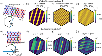
In a recent work Shah et al. (2021), we have provided an interpretation of the backscattering transitions in valley Hall waveguides as tunneling transitions in the quasi-momentum space. Our previous investigation focused on smooth domain walls. In this work, we move our attention to systems with hard domain walls (i.e. system in which the underlying crystal geometry changes abruptly at the domain wall) and consider a regime where the transverse confinement is relatively strong. In particular, we are interested in experimentally relevant scenarios in which two or more straight waveguides are connected at sharp corners, cf Fig.1(a). We find that the transport and spectral properties are highly sensitive on the orientation of the waveguides. Extensive simulations of the density of states (DOS) of straight waveguides as well as of the transmission at a sharp corner give hints of an underlying fractal dependence of these observables on the energy and the waveguide orientation. We provide an explanation of these empirical observations by analyzing the quasi-momentum paths and energies for resonant tunneling.
The fractal spectrum we analyze is reminiscent of the Butterfly spectrum of 2D charge particles on a lattice as a function of the magnetic flux originally predicted by Hofstadter Hofstadter (1976) and later observed in a variety of platforms including graphene superlattices Dean et al. (2013); Ponomarenko et al. (2013), cold atoms in optical lattices Aidelsburger et al. (2013), and superconducting qubits Roushan et al. (2017). In our work, the orientation of the waveguide relative to the lattice plays a similar role as the magnetic flux. Our work is also loosely connected to the investigation of fractal spectra in quasi-crystal geometries Zilberberg (2021); Kraus et al. (2012); Verbin et al. (2013); Tran et al. (2015); Bandres et al. (2016) . Indeed, the waveguides we investigate can be viewed as 1D quasi-crystals for orientations that are not commensurate to the lattice. However, we emphasize that, here, the fractal structure we describe is not a property of the spectrum for a single orientation but rather of its variation as a function of the orientation.
II Review of the valley Hall physics
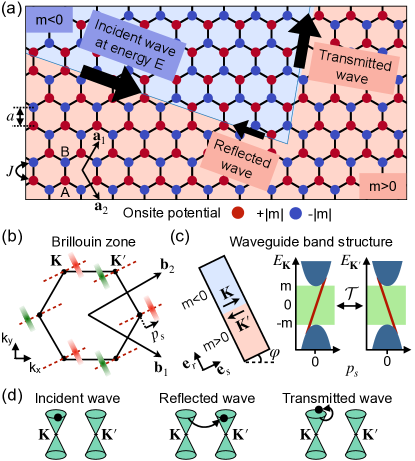
In order to set the stage for our work, we start giving a brief introduction to the valley Hall physics. For this purpose and, more generally, as a case study for our investigation we introduce the simplest toy model that allows to implement valley Hall guided modes. This model is a simple extension of nearest-neighbors graphene tight-binding model as detailed below.
Excitations on a honeycomb lattice hops with rate between nearest-neighbors sites with opposite onsite energies, and on sublattices A and B, respectively. We allow the amplitude and sign of the mass parameter to depend on the unit cell. In this way, the lattice can be viewed as being divided into distinct domains according to the sign of the mass parameter, cf Fig. 1a. We, thus, arrive to the simple tight-binding Hamiltonian
| (1) |
Here, indicates the unit cell position and, thus, it is a lattice vector, with integers and unit lattice vectors, . In addition, denotes the sum over nearest-neighbors.
II.1 Quasi-momentum representation
To gain insight on the valley Hall physics and in particular the phenomenon of backscattering (discussed below), it is very useful to introduce the quasi-momentum representation. To switch to the quasi-momentum representation we project the valley Hall Hamiltonian Eq. (1) into a basis of plane waves ,
| (2) |
where is a set of Pauli matrices acting on the sublattice degree of freedom, , , and is given by
| (3) |
We note that the quasi-momentum is defined modulus a reciprocal lattice vector and can be chosen within the Brillouin zone of area , cf Fig. 1(b). Thus, the normal modes (in quasi-momentum space) are periodic eigenstates of Eq. (3),
with and unit vectors of the reciprocal lattice.
II.2 Dirac Hamiltonian and valley Chern numbers
For the bulk case, , the quasi-momentum is a constant of motion and reduces to a simple matrix. Its spectrum as a function of the quasi-momentum defines the band structure given by
| (4) |
In the special case , it features Dirac cones centered at the Dirac high-symmetry points and . A finite mass opens a band gap of width between the two bands. We note that the band structure is independent of the sign of the mass parameter . However, this quantity is still very important in that it determines the symmetry-properties of the underlying normal modes.
Next, we focus our attention on exitations whose wavefunction is localized in a so-called valley, i.e. the vicinity of a Dirac point. The dynamics of these Valley-polarized excitations are captured by a Dirac equation obtained by expanding the Hamiltonian Eq. (3) about the relevant Dirac point. For the -valley, the Dirac equation reads
| (5) |
Here, is the quasi-momentum counted off from the high-symmetry point . We note in passing that the Dirac equation can also be derived from symmetry consideration in the framework of a smooth-envelope approximation without any detailed knowledge of the underlying microscopic model, see e.g. Shah et al. (2021). For the bulk case , it is possible to associate to the Dirac Hamiltonian a topological invariant the so-called valley Chern numbers Martin et al. (2008). The valley Chern number assumes two possible half-integer values or , with opposite signs in the two valleys. For the lowest band and the -valley, we have . Under the assumption that the Berry curvature is peaked in the region of validity of the Dirac equation (which is true as long as ), the valley Chern numbers accurately quantifies the contribution from a valley to the overall band Chern number.
II.3 Topological guided modes
When a domain with positive mass is joined to a domain with negative mass, cf Fig. 1(a), the valley Chern number across the surface changes by one unit. In this scenario, the bulk boundary correspondence separately applied to each valley (with the implicit assumption that the two valleys are not coupled), predicts the appearance of a pair of guided counter-propagating gapless modes (one mode for each valley). Thus, we can view such a domain wall configuration as a topological waveguide.
The appearance of guided modes at the interface of two regions with opposite sign of the mass parameter can also be substantiated by directly diagonalizing the Dirac Hamiltonian (5). Indeed, the existence of a guided mode for the Dirac equation in the presence of a straight domain wall has been originally predicted by Jackiw and Rebbi Jackiw and Rebbi (1976). If we choose a set of coordinates and such that with the domain wall on the axis and in the lower-half plane, cf Fig. 1(c), the guided mode has energy dispersion
| (6) |
Here, is the Dirac velocity and is the component of the quasimomentum longitudinal to the domain wall, where is the unit vector in the longitudinal direction. State of the art experimental realizations normally feature hard domain walls, where is the coordinate transverse to the domain wall, cf Fig. 1(c). In this case, the Jackiw and Rebbi solution has wavefunction
| (7) |
Here, is the angular-coordinate of the mass domain wall, cf Fig. 1(c). The guided mode for the valley is obtained by applying the time-reversal operator (in this case complex conjugation) to Eq. (7), .
It is instructive to rewrite the guided mode wavefunction in the quasimomentum representation . We find
| (8) |
Here, is the unit vector in the radial direction, cf Fig.1(c). Thus, the right propagating guided mode is localised about the quasimomentum with standard deviation in the transverse direction. On the other hand, the time-reversed solution in the ’-valley will be localized about , see the geometrical illustration in Fig. 1(b). We note that for , is much smaller than the distance between the two valleys.
We now consider a setup where two straight waveguides have been connected by a sharp corner, cf Fig. 1(a). If the condition is fulfilled, the quasimomentum transfer after turning the corner is much smaller than the quasimomentum transfer that would be required for backscattering, cf Fig. 1(d). This leads to suppression of backscattering and, thus, robust transport.
We note that there is a trade off between the bandwidth for the guided modes and how well backscattering is suppressed (or, equivalently, how strongly the guided modes are localized in quasimomentum) Shah et al. (2021). In order to boost the bandwidth, many experiments are realized in a regime of intermediate values of the dimensionless bulk mass parameter in which the coupling between the two valleys can not be safely neglected, see e.g. Shaley et al. Shalaev et al. (2019), Zeng et al. Zeng et al. (2020), Ren et al. Ren et al. (2022), Ma et al. Ma et al. (2021), and Arora et al. Arora et al. (2021) with , respectively. This has motivated us to investigate the regime of intermediate masses directly diagonalizing numerically Eq. (1) and, thus, accounting also for the coupling between the two valleys. In all simulation below, we have used the dimensionless bulk mass parameter . We expect qualitatively similar results for similar values of .
III Tunneling induced band gaps in valley Hall waveguides
The simplest signature of the coupling between the two valleys (beyond the Dirac equation approach) is the appearance of minigaps in the band structure of a straight waveguide. These band gaps have been investigated in Shah et al. (2021) with a special focus on the case of smooth mass domain walls . This work has also shown that there is a deep connection between these band gaps and backscattering in a closed domain wall. For this reason, we also start investigating the band structure for straight waveguides before switching to the problem of backscattering at sharp corners in Section V. Our investigation is complementary to Shah et al. (2021) in that we focus on the case of sharp domain walls and corners.
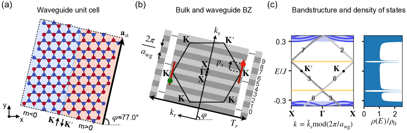
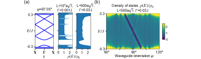
In the Dirac Hamiltonian approach, the momentum counted off from the corresponding high-symmetry point is formally treated as a continuous variable, . This leads to quantized valley Chern numbers and a simple description with a continuous dependence of energy and wavefunction on the angular coordinate , cf Eqs. (6,7). We note, however, that the longitudinal quasi-momentum is not a conserved quantity. A full numerical evaluation (beyond the Dirac equation) of a waveguide’s band structure can be straightforwardly performed whenever the waveguide is translationally invariant. This allows to define a waveguide lattice constant , cf Fig. 2(a), and the corresponding conserved waveguide quasimomentum , Fig. 2(b). In particular, the Jackiew and Rebbi solution in the valley has waveguide quasimomentum while its time-reversed partner in the valley has opposite quasimomentum, . Thus, the two solutions, which have the same energy, have also the same waveguide quasi-momentum at the time-reversal invariant high-symmetry points or . At these points, they are resonantly coupled leading to a gap in the guided mode band structure. The band gap can be viewed as a tunnel splitting proportional to the overlap of the two guided modes , and which are peaked in different valleys Shah et al. (2021). In this framework, the peaks quasimomenta and (see definition above) can be viewed as the classical quasimomenta of the two counter-propagating guided modes (a rigorous WKB approach is possible for smooth domain walls Shah et al. (2021)). The resulting band structure, for the special case , is shown in Fig. 2(c). An alternative representation of the spectrum is provided by the density of states (DOS) , Fig. 2(d). For an infinite size system, the DOS in the region of the bulk band gap is flat away from the guided modes band gaps, vanishes inside the band gaps, and displays Van Howe singularities at the band edges, cf Fig. 2(d). Numerically, we suppress finite size artifacts by simulating a large system size in the presence of a small homogeneous broadening of the energy levels, see Appendix A.
Until now we have focused on translationally invariant waveguides. Thus, we have implicitly assumed that the mass domain wall is aligned with at least one lattice vector . This is the case only for angles fulfilling the rationality condition Charlier et al. (2007)
| (9) |
with and relative prime integers. The waveguide lattice constant is then
| (10) |
We note that the lattice constant is a discontinuous function of via and . Thus, the number of bands and band gaps will also be a discontinuous function of leading to an overall discontinuous spectrum. This is reminiscent of the discontinuous dependence of the energy spectrum of electrons in an external magnetic field as a function of the magnetic flux Hofstadter (1976). In the latter scenario, the appearance of an ever larger number of band gaps for large denominators of the magnetic flux leads to the celebrated Hofstadter butterfly spectrum Hofstadter (1976). This spectrum has been intriguing for generation of researchers and even the general public because of its self-similar fractal nature. This has motivated us to explore numerically the edge state spectrum as a function of the angular-coordinate .
IV Fractal orientation-dependence of the band structure
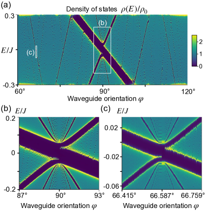
The DOS of the waveguide as a function of energy and orientation is shown in Fig. 3(a). We focus on the interval as the DOS for angles outside of this interval can be recovered by applying the following symmetry considerations: (i) A rotation by of the domain wall is equivalent to a rotation of the whole Hamiltonian and, thus, does not change the spectrum, (ii) A rotation by of the domain wall just changes the sign of all onsite energies. Since the lattice is bipartite each energy level has a corresponding level with opposite energy in the rotated structure, . As it should be expected given the discontinuous -dependence of the number of band gaps, the density of states displays an intricate structure. A multitude of band gaps (dark blue strips) of varying width merge at the intersection of the and -axes with the two main band gaps forming an x-shaped pattern, cf also the zoom in Fig. 3(b). Surprisingly further magnification about the intersection of the axis and reveals that the same remarkable pattern is repeated for smaller energy and angle variations, cf Fig. 3(c). This raises the question whether further magnification would reveal a self-repeating fractal pattern, analogous to the celebrated Hofstadter’s Butterfly spectrum but now with the angle playing the role of the magnetic flux. We investigate this question in the next section.
We note in passing that for any fixed irrational the waveguide can be viewed as a quasicrystal Lifshitz (2003); Senechal (2009); Zilberberg (2021). Quasicrystals have been shown to support fractal band structures Bandres et al. (2016); Zilberberg (2021). In our setting such non-commensurate orientations supports an infinite number of band gaps Shah et al. (2021). So it is at least conceivable that the band structure for a fixed irrational angle could also be a fractal. Here, we leave this as an interesting open question and rather focus on the orientation dependence of the spectrum.
IV.1 Resonant tunneling for arbitrary waveguide orientation
From Fig. 3(a) it is clear that even though the number of band gaps is a discontinuous function of the orientation , each given band gap can be viewed as defining a continuous function. In this section, we give a theoretical underpinning to this observation by following the approach of Ref. Shah et al. (2021).
In the quasi-momentum representation, the wavefunction of the guided mode for an arbitrary (possibly irrational) can be found using the ansatz
| (11) |
Here, () is the quasimomentum in the direction longitudinal (transverse) to the domain wall, cf Fig. 2(a,b). For rational (corresponding to translationally invariant waveguides, cf Eq. (9)) this is just a Bloch-wave ansatz with waveguide quasimomentum . More in general, can be viewed as a label for the support manifold of the function . This is a submanifold of the BZ parameterized by the radial quasi-momentum . When the quasi-momentum is taken inside the hexagonal Brillouin zone such submanifold transverse the BZ multiple times (for irrational infinitely many times) defining a series of parallel lines, cf blue lines in the BZs depicted in Fig. 4(b,c). For rational , it is a closed manifold of length . We note that the Jackiw and Rebbi solution Eq. (8) represents a special example of the ansatz Eq. (11) with the additional assumption that the wavefunction is peaked close to the -point. We mention in passing that a more general guided solution localized about a quasimomentum that is not necessarily close to any high-symmetry point has been derived in Ref. Shah et al. (2021). Interestingly, this guided solution is unique (up to a reparametrization of ) and can be viewed as defining a single band comprising a right and a left propagating branch. As for the Jackiw and Rebbi solution, both the energy dispersion and the classical quasi-momentum depend only on but not on . For close to the middle of the bulk band gap, the classical quasimomentum is close to a Dirac point recovering the Jackiw and Rebbi solution.
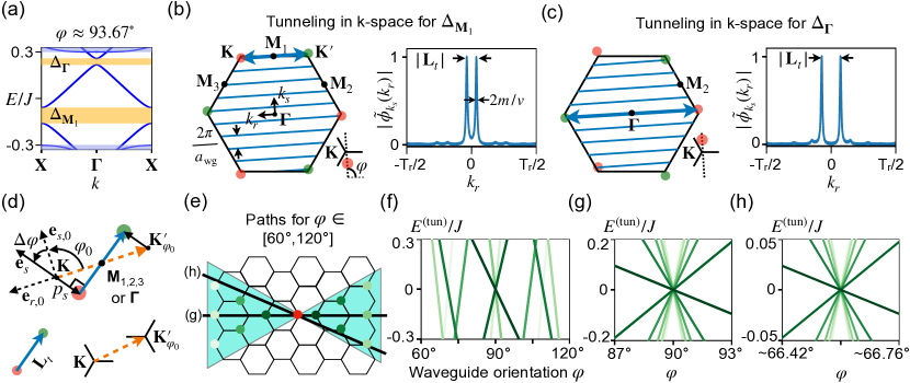
The emergence of the minigaps, forming the intricate pattern in Fig. 3 is the consequence of the tunneling induced hybridization of time-reversal-partner solutions localized about two opposite and possibly distant quasi-momenta, cf Fig. 4(b,c). In section III we have explained that for translationally invariant waveguides, the tunneling is resonant at the time-reversal-symmetric (waveguide) quasi-momenta , and . For arbitrary waveguides, Ref. Shah et al. (2021) identified a more general condition: the two time-reversed solutions should have support on the same submanifold (but will be peaked at different ). This submanifold is itself time-reversal invariant. For irrational (rational) , the time-reversal invariant manifolds pass through one (two) time-reversal invariant honeycomb lattice quasi-momentum (quasimomenta), or , cf Fig. 4(d). In either scenario (rational or irrational ) one can identify a dominant tunneling path, on which the overlap of the localized solutions is largest. This path (indicated by the thick blue line in Fig. 4(b-d)) connects the two classical quasi-momenta via a single time-reversal invariant quasimomentum. Two key intuitions allow to shed light on the intricate DOS pattern in Fig. (3). First, each continuous minigap is associated to a specific continuous (as a function of ) tunneling path. Each such path (and the corresponding minigap) can be labeled with a time-reversal-invariant high-symmetry point (one of the -points or the -point) and the number of times it traverses each valley Shah et al. (2021), cf Fig. 4(a-c). Second, the different minigaps are of very different magnitudes. Quantifying these magnitudes is technically difficult as it requires to calculate the tail of the Jackiw and Rebbi solutions in quasi-momentum space, going beyond the Dirac equation treatment Shah et al. (2021). However, for a qualitative understanding of the DOS patterns observed in Fig. 3, it is enough to observe that there is a correlation between the size of a band gap and the length of the tunneling path, with longer tunneling paths leading to smaller band gaps, cf Fig. 4(a-c). Thus, only a finite number of the infinitely many band gaps appears in a smeared out DOS, cf Fig. 3.
IV.2 Explanation of the fractal pattern
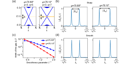
Next, we focus on the guided modes spectrum in the region centered about where the interesting multiscale pattern is observed, cf Fig. (3). Our approach is centered on special tunneling paths that are associated to tunneling transitions that are resonant for exactly zero energy. In other words, they give rise to a minigap with center energy for an appropriate waveguide orientation . We refer to these tunneling paths as zero-energy tunneling paths. By analyzing their properties we will be able to show that the same pattern for the center energies of the minigaps as a function of the angles repeats infinitely many times about the axis for ever smaller energy and angle variations, overall, forming a self-similar fractal pattern.
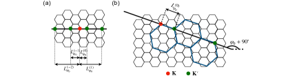
About zero-energy we can determine the resonant tunneling energy using the Jackiw and Rebbi solution Eqs. (6,8). We preliminary note that for any arbitrary the guided mode energy always has as classical quasi-momentum a Dirac point, or . The two solutions at and are time-reversal partners and the tunneling between them becomes resonant whenever a tunneling paths orthogonal to the waveguide orientation connects these two high symmetry points. Geometrically, we can represent these zero-energy tunneling paths as described below. As a preliminary step, we draw the lattice that contains all momenta corresponding to the or the -points, cf Fig. 4(e). This is a honeycomb lattice in reciprocal space which has as lattice vectors the reciprocal lattice vectors . Each zero-energy tunneling paths (once unfolded into the -plane) can be represented as a straight line connecting a fixed momentum on the -sublattice (e.g. the red point in Fig. 4(e)) with one of the infinite many momenta on the -lattice. In Fig. 4(e), we highlight the region of reciprocal space that hosts the zero-energy tunneling path for the waveguides orientations in the interval . In this region, we also highlight the momenta on the -lattice with different shades of green, encoding the length of the tunnelling path connecting these sites to the red dot on the -lattice. (As discussed above shorter paths correspond to larger band gaps.) Since the corresponding waveguide orientation is orthogonal to the zero-energy tunneling path and, at the same time, the reciprocal lattice is rotated by compared to the real space lattice, we conclude that a waveguide supports a zero-energy band gap if and only if moving in the longitudinal direction from a point on the sublattice one eventually crosses a point on the sublattice. While these particular set of orientations are a dense subset of the angles corresponding to translationally invariant waveguides (and hence a dense subset of all orientations), in practice, only a finite and well spaced subset of orientations (those supporting the shortest zero-energy tunneling paths) will give rise to zero-energy band gaps in a smeared out density of states, as shown in Fig. 3.
After having identified the waveguide orientations giving rise to large band gaps centered around zero energy, we want to understand the structure of the density of states in the vicinity of these special orientations. We denote one such orientation as . We also introduce the vectors and longitudinal and transverse to the domain wall [with the same conventions as in Fig. 1(c)], and the momentum on the -lattice such that the vector is orthogonal to . Simple geometrical considerations, cf Fig. 4(d), show that the linear dispersion of the Jackiew and Rebbi solution Eq. (6) gives rise to a linear dependence of the resonant tunneling energy on the waveguide orientation counted off from ,
| (12) |
Here, is the projection of the zero-energy tunneling path along the -axis, (equivalently, this is the length of the zero-energy tunneling path multiplied by the appropriate sign). This formula allows to predict the slope of the band gap center for each band gap that crosses zero energy in terms of the zero-energy tunneling path or, equivalently, the corresponding and end momenta. As explained above the width of the band gap is proportional to the tunneling length and, in practice, only the shortest tunneling paths will give rise to appreciable band gaps. The band gap centers for the shortest zero-energy tunneling paths (those corresponding to the momenta highlighted as green dots in Fig. 4(e)) calculated using Eq. (12) are shown in Fig. 4(f). We note that several band gaps merge at the same origin on the zero-energy axis as previously observed for the density of states in Fig. (3). This simply reflects that there are (infinitely) many momenta on every line that also crosses a momentum, cf Fig. 4(e). Geometrical considerations shows that if we label these momenta with an integer label choosing for the shortest zero-energy tunneling path (for a fixed ) the other labels can be chosen such that
| (13) |
with see Appendix B. In other words the ratio is independent on . This relation can be rephrased more generally as a constraint on the coordinates of the sites of a honeycomb lattice, see Appendix B. In our setting, the parameters set the slope of the tunneling energies , given by Eq. (12) with . Thus, the local pattern of the resonant tunneling energies about a zero-energy tunneling orientation is always the same, with the angle only fixing the scale via , cf Fig. 4(g-h). Overall, in the ideal limit of an infinite system without dissipation, this induce a self-similar fractal pattern for the tunneling energies as a function of the waveguide orientation .
Until now we have analysed the fractal pattern for the tunneling energies as a function of the waveguide orientation. Next, we discuss how a similar pattern is imprinted in the DOS. We note that our analysis so far only partially explains the empirical observation that exactly the same pattern is observed in the DOS at two different scales, cf Figs. 3(b,c). In particular, it accounts for the slopes of the band gaps but not for their widths. While we expect that the widths (set by the underlying tunneling rate) will be proportional to the length of the zero-energy tunneling path, the dependence will in general be non-linear. For this reason, zoom-ins of the DOS about different may look substantially different even after accounting for the different scale factors. Nevertheless, they will all display a series of band gaps of varying width merging at zero energy. Thus, the overall global dependence of the DOS on the waveguide orientation inherits the self-repeating fractal nature of the resonant tunneling energies.
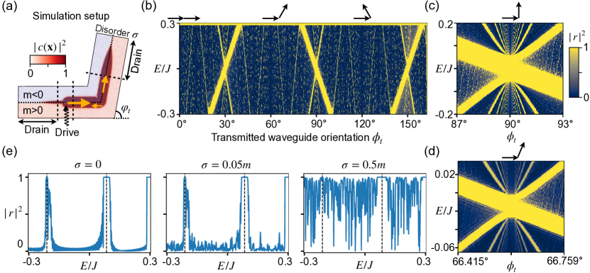
V Fractal transmission at a sharp corner
Next, we analyze a transport scenario that would allow to directly observe the fractal features analyzed so far. We consider a setup formed by connecting two waveguides of different orientations via a sharp corner, see Figs. 1 and 5(a). We are mainly interested in the dependence of the transmission on the waveguides orientations. We mention in passing that in the hard domain-wall scenario considered here, the exact location of the domain wall relative to the lattice can also influence the transmission quantitatively (see Appendix C). However, no qualitative change is observed indicating that the smooth envelope approximation is sufficient to capture the essential physics of the problem.
The simulation setup is shown in Fig. 5(a). We drive two sites on the initial waveguide with the same amplitude and frequency (energy), but a suitable phase difference, to unidirectionally excite the edge channel towards the corner (see Appendix D). At the corner, the wave is partially backscattered. Eventually, the transmitted and the reflected waves are absorbed in two different drains. To prevent any undesirable backscattering at the drain-waveguide interface, the dissipation rate is increased very slowly in the drains, see Appendix D for more details. Therefore, we need large drains, which results in a tight-binding model of lattice sites. We use sparse matrices to store and perform linear algebra operations on such large dimensional matrices. We derive the steady state backscattering rate from the ratio of the absorbed intensities in the transmission and absorption drains, see Appendix D. We choose the first waveguide to support a zig-zag domain wall () because this configuration does not feature a band gap for the parameters considered here. In this way, an excitations of frequency inside the bulk band gap can always be injected in the first waveguide and will only be backscattered if its frequency is in the band gap of the second waveguide. A more complex scenario with a different initial waveguide orientation is described in the Appendix E. The backscattering rate as a function of the energy and the final waveguide orientation is shown Fig. 5(b). As expected, the backscattering rate spikes up whenever the final waveguide band structure has a band gap at that energy. Moreover, Fig. 5(c,d) features a similar fractal pattern as that in Fig. 3. To mimic a realistic experimental systems, we introduce disorder in the onsite potentials of the lattice sites. We observe that the fractal pattern is roughly intact up to disorder levels an order of magnitude smaller than the bulk band gap , see Fig. 5(e).
VI Discussion and outlook
Our investigation of the orientation dependence of the density of state and transmission in valley Hall waveguides has focused on a specific case study, a simple extension of the graphene tight-binding model. Nevertheless, the physics described here is robust and extends beyond the validity of this specific model. Importantly, we have relied on it only for our numerical calculations. On the other hand, we have explained the repeating pattern featuring multiple waveguide’s band gaps merging in the middle of the bulk band gap solely based on the effective Dirac Hamiltonian Eq. (5) and the position of the Dirac cones in the crystal BZ (which is fixed by the underlying space group). We can conclude that a qualitatively similar pattern will be observed in any valley Hall waveguide with the suitable space group symmetries of the bulk crystal structure (at least or before introducing the gap-opening perturbation, see e.g. Shah et al. (2022)). More precisely, the centers of the band gaps are captured by Eq. (5) while the widths depend on the tails of the guided modes and, thus, on the microscopic wave equations. Reconfigurable implementations of topological waveguides Fleury et al. (2016); Cheng et al. (2016); Zhang et al. (2018a); Zhao et al. (2019); Darabi et al. (2020); Tian et al. (2020) are ideally suited to verify our predictions.
More generally, we expect that the physics investigated, here, to be relevant for other topological waveguides obtained using a variety of schemes based on the geometric engineering of crystal structures supporting Dirac cones Shah et al. (2022). In this more general setting, the counter-propagating guided modes are usually described within a smooth-envelope approximation that does not capture their coupling via their tails. This coupling becomes significant in the regime of tight transverse confinement/large band gaps, . In this regime, we expect that tunneling induced band gaps can be observed. As for the valley Hall waveguides investigated in this work, the number of band gaps will depend discontinuously on the waveguide orientation leading to qualitatively different but similarly intricated patterns with merging band gaps for the band structure/transmission vs waveguide orientation.
We are confident that our investigation provides a significant contribution toward the general goal of achieving efficient routing of photons or phonons along arbitrary paths in densely-packed integrated circuits.
Acknowledgements
T.S. acknowledges support from the European Union’s Horizon 2020 research and innovation programme under the Marie Sklodowska-Curie grant agreement No. 722923 (OMT). F.M. acknowledges support from the European Union’s Horizon 2020 Research and Innovation program under Grant No. 732894, Future and Emerging Technologies (FET)-Proactive Hybrid Optomechanical Technologies (HOT).
References
- Hasan and Kane (2010) M. Z. Hasan and C. L. Kane, “Colloquium : Topological insulators,” Reviews of Modern Physics 82, 3045–3067 (2010).
- Bernevig et al. (2006) B. Andrei Bernevig, Taylor L. Hughes, and Shou-Cheng Zhang, “Quantum Spin Hall Effect and Topological Phase Transition in HgTe Quantum Wells,” Science 314, 1757–1761 (2006).
- Kane and Mele (2005) C. L. Kane and E. J. Mele, “Quantum Spin Hall Effect in Graphene,” Phys. Rev. Lett. 95, 226801 (2005).
- Ozawa et al. (2019) Tomoki Ozawa, Hannah M. Price, Alberto Amo, Nathan Goldman, Mohammad Hafezi, Ling Lu, Mikael C. Rechtsman, David Schuster, Jonathan Simon, Oded Zilberberg, and Iacopo Carusotto, “Topological photonics,” Reviews of Modern Physics 91, 015006 (2019).
- Shah et al. (2022) Tirth Shah, Christian Brendel, Vittorio Peano, and Florian Marquardt, “Topologically Protected Transport in Engineered Mechanical Systems,” (2022), arXiv:2206.12337 [cond-mat].
- Martin et al. (2008) Ivar Martin, Ya. M. Blanter, and A. F. Morpurgo, “Topological Confinement in Bilayer Graphene,” Physical Review Letters 100, 036804 (2008).
- Ju et al. (2015) Long Ju, Zhiwen Shi, Nityan Nair, Yinchuan Lv, Chenhao Jin, Jairo Velasco, Claudia Ojeda-Aristizabal, Hans A. Bechtel, Michael C. Martin, Alex Zettl, James Analytis, and Feng Wang, “Topological valley transport at bilayer graphene domain walls,” Nature 520, 650–655 (2015).
- Wu et al. (2017) Xiaoxiao Wu, Yan Meng, Jingxuan Tian, Yingzhou Huang, Hong Xiang, Dezhuan Han, and Weijia Wen, “Direct observation of valley-polarized topological edge states in designer surface plasmon crystals,” Nature Communications 8, 1304 (2017).
- Ma and Shvets (2016) Tzuhsuan Ma and Gennady Shvets, “All-Si valley-Hall photonic topological insulator,” New Journal of Physics 18, 025012 (2016).
- Dong et al. (2017) Jian-Wen Dong, Xiao-Dong Chen, Hanyu Zhu, Yuan Wang, and Xiang Zhang, “Valley photonic crystals for control of spin and topology,” Nature Materials 16, 298–302 (2017).
- Gao et al. (2017) Zhen Gao, Zhaoju Yang, Fei Gao, Haoran Xue, Yahui Yang, Jianwen Dong, and Baile Zhang, “Valley surface-wave photonic crystal and its bulk/edge transport,” Physical Review B 96, 201402 (2017).
- Kang et al. (2018) Yuhao Kang, Xiang Ni, Xiaojun Cheng, Alexander B. Khanikaev, and Azriel Z. Genack, “Pseudo-spin–valley coupled edge states in a photonic topological insulator,” Nature Communications 9, 3029 (2018).
- Noh et al. (2018) Jiho Noh, Sheng Huang, Kevin P. Chen, and Mikael C. Rechtsman, “Observation of Photonic Topological Valley Hall Edge States,” Physical Review Letters 120, 063902 (2018).
- Shalaev et al. (2019) Mikhail I. Shalaev, Wiktor Walasik, Alexander Tsukernik, Yun Xu, and Natalia M. Litchinitser, “Robust topologically protected transport in photonic crystals at telecommunication wavelengths,” Nature Nanotechnology 14, 31–34 (2019).
- Zeng et al. (2020) Yongquan Zeng, Udvas Chattopadhyay, Bofeng Zhu, Bo Qiang, Jinghao Li, Yuhao Jin, Lianhe Li, Alexander Giles Davies, Edmund Harold Linfield, Baile Zhang, Yidong Chong, and Qi Jie Wang, “Electrically pumped topological laser with valley edge modes,” Nature 578, 246–250 (2020).
- Arora et al. (2021) Sonakshi Arora, Thomas Bauer, René Barczyk, Ewold Verhagen, and L. Kuipers, “Direct quantification of topological protection in symmetry-protected photonic edge states at telecom wavelengths,” Light: Science & Applications 10, 9 (2021).
- Lu et al. (2017) Jiuyang Lu, Chunyin Qiu, Liping Ye, Xiying Fan, Manzhu Ke, Fan Zhang, and Zhengyou Liu, “Observation of topological valley transport of sound in sonic crystals,” Nature Physics 13, 369–374 (2017).
- Vila et al. (2017) Javier Vila, Raj Kumar Pal, and Massimo Ruzzene, “Observation of topological valley modes in an elastic hexagonal lattice,” Physical Review B 96, 134307 (2017).
- Xia et al. (2018) Bai-Zhan Xia, Sheng-Jie Zheng, Ting-Ting Liu, Jun-Rui Jiao, Ning Chen, Hong-Qing Dai, De-Jie Yu, and Jian Liu, “Observation of valleylike edge states of sound at a momentum away from the high-symmetry points,” Physical Review B 97, 155124 (2018).
- Zhang et al. (2018a) Zhiwang Zhang, Ye Tian, Ying Cheng, Qi Wei, Xiaojun Liu, and Johan Christensen, “Topological Acoustic Delay Line,” Physical Review Applied 9, 034032 (2018a).
- Zhang et al. (2018b) Zhiwang Zhang, Ye Tian, Yihe Wang, Shuxiang Gao, Ying Cheng, Xiaojun Liu, and Johan Christensen, “Directional Acoustic Antennas Based on Valley-Hall Topological Insulators,” Advanced Materials 30, 1803229 (2018b).
- Tian et al. (2020) Zhenhua Tian, Chen Shen, Junfei Li, Eric Reit, Hunter Bachman, Joshua E. S. Socolar, Steven A. Cummer, and Tony Jun Huang, “Dispersion tuning and route reconfiguration of acoustic waves in valley topological phononic crystals,” Nature Communications 11, 762 (2020).
- Ren et al. (2022) Hengjiang Ren, Tirth Shah, Hannes Pfeifer, Christian Brendel, Vittorio Peano, Florian Marquardt, and Oskar Painter, “Topological phonon transport in an optomechanical system,” Nature Communications 13, 3476 (2022).
- Ma et al. (2021) Jingwen Ma, Xiang Xi, and Xiankai Sun, “Experimental Demonstration of Dual‐Band Nano‐Electromechanical Valley‐Hall Topological Metamaterials,” Advanced Materials 33, 2006521 (2021).
- Zhang et al. (2021) Zi-Dong Zhang, Si-Yuan Yu, Hao Ge, Ji-Qian Wang, Hong-Fei Wang, Kang-Fu Liu, Tao Wu, Cheng He, Ming-Hui Lu, and Yan-Feng Chen, “Topological Surface Acoustic Waves,” Physical Review Applied 16, 044008 (2021).
- Xi et al. (2021) Xiang Xi, Jingwen Ma, Shuai Wan, Chun-Hua Dong, and Xiankai Sun, “Observation of chiral edge states in gapped nanomechanical graphene,” Science Advances 7, eabe1398 (2021).
- Zhang et al. (2022) Qicheng Zhang, Daehun Lee, Lu Zheng, Xuejian Ma, Shawn I. Meyer, Li He, Han Ye, Ze Gong, Bo Zhen, Keji Lai, and A. T. Charlie Johnson, “Gigahertz topological valley Hall effect in nanoelectromechanical phononic crystals,” Nature Electronics 5, 157–163 (2022).
- Shah et al. (2021) Tirth Shah, Florian Marquardt, and Vittorio Peano, “Tunneling in the Brillouin zone: Theory of backscattering in valley Hall edge channels,” Physical Review B 104, 235431 (2021).
- Hofstadter (1976) Douglas R. Hofstadter, “Energy levels and wave functions of Bloch electrons in rational and irrational magnetic fields,” Physical Review B 14, 2239–2249 (1976).
- Dean et al. (2013) C. R. Dean, L. Wang, P. Maher, C. Forsythe, F. Ghahari, Y. Gao, J. Katoch, M. Ishigami, P. Moon, M. Koshino, T. Taniguchi, K. Watanabe, K. L. Shepard, J. Hone, and P. Kim, “Hofstadter’s butterfly and the fractal quantum Hall effect in moiré superlattices,” Nature 497, 598–602 (2013).
- Ponomarenko et al. (2013) L. A. Ponomarenko, R. V. Gorbachev, G. L. Yu, D. C. Elias, R. Jalil, A. A. Patel, A. Mishchenko, A. S. Mayorov, C. R. Woods, J. R. Wallbank, M. Mucha-Kruczynski, B. A. Piot, M. Potemski, I. V. Grigorieva, K. S. Novoselov, F. Guinea, V. I. Fal’ko, and A. K. Geim, “Cloning of Dirac fermions in graphene superlattices,” Nature 497, 594–597 (2013).
- Aidelsburger et al. (2013) M. Aidelsburger, M. Atala, M. Lohse, J. T. Barreiro, B. Paredes, and I. Bloch, “Realization of the Hofstadter Hamiltonian with Ultracold Atoms in Optical Lattices,” Physical Review Letters 111, 185301 (2013).
- Roushan et al. (2017) P. Roushan, C. Neill, J. Tangpanitanon, V. M. Bastidas, A. Megrant, R. Barends, Y. Chen, Z. Chen, B. Chiaro, A. Dunsworth, A. Fowler, B. Foxen, M. Giustina, E. Jeffrey, J. Kelly, E. Lucero, J. Mutus, M. Neeley, C. Quintana, D. Sank, A. Vainsencher, J. Wenner, T. White, H. Neven, D. G. Angelakis, and J. Martinis, “Spectroscopic signatures of localization with interacting photons in superconducting qubits,” Science 358, 1175–1179 (2017).
- Zilberberg (2021) Oded Zilberberg, “Topology in quasicrystals [Invited],” Optical Materials Express 11, 1143 (2021).
- Kraus et al. (2012) Yaacov E. Kraus, Yoav Lahini, Zohar Ringel, Mor Verbin, and Oded Zilberberg, “Topological States and Adiabatic Pumping in Quasicrystals,” Physical Review Letters 109, 106402 (2012).
- Verbin et al. (2013) Mor Verbin, Oded Zilberberg, Yaacov E. Kraus, Yoav Lahini, and Yaron Silberberg, “Observation of Topological Phase Transitions in Photonic Quasicrystals,” Physical Review Letters 110, 076403 (2013).
- Tran et al. (2015) Duc-Thanh Tran, Alexandre Dauphin, Nathan Goldman, and Pierre Gaspard, “Topological Hofstadter insulators in a two-dimensional quasicrystal,” Physical Review B 91, 085125 (2015).
- Bandres et al. (2016) Miguel A. Bandres, Mikael C. Rechtsman, and Mordechai Segev, “Topological Photonic Quasicrystals: Fractal Topological Spectrum and Protected Transport,” Physical Review X 6, 011016 (2016).
- Jackiw and Rebbi (1976) R. Jackiw and C. Rebbi, “Solitons with fermion number,” Physical Review D 13, 3398–3409 (1976).
- Charlier et al. (2007) Jean-Christophe Charlier, Xavier Blase, and Stephan Roche, “Electronic and transport properties of nanotubes,” Reviews of Modern Physics 79, 677–732 (2007).
- Lifshitz (2003) Ron Lifshitz, “Quasicrystals: A Matter of Definition,” Foundations of Physics 33, 1703–1711 (2003).
- Senechal (2009) Marjorie Senechal, Quasicrystals and geometry, re-issued in this digitally printed version ed. (Cambridge University Press, Cambridge, 2009).
- Fleury et al. (2016) Romain Fleury, Alexander B. Khanikaev, and Andrea Alu, “Floquet topological insulators for sound,” Nature Communications 7, 11744 (2016).
- Cheng et al. (2016) Xiaojun Cheng, Camille Jouvaud, Xiang Ni, S. Hossein Mousavi, Azriel Z. Genack, and Alexander B. Khanikaev, “Robust reconfigurable electromagnetic pathways within a photonic topological insulator,” Nature Materials 15, 542–548 (2016).
- Zhao et al. (2019) Han Zhao, Xingdu Qiao, Tianwei Wu, Bikashkali Midya, Stefano Longhi, and Liang Feng, “Non-Hermitian topological light steering,” Science 365, 1163–1166 (2019).
- Darabi et al. (2020) Amir Darabi, Xiang Ni, Michael Leamy, and Andrea Alù, “Reconfigurable Floquet elastodynamic topological insulator based on synthetic angular momentum bias,” Science Advances 6, eaba8656 (2020).
Appendix A Calculation of density of states
In this section, we describe how to evaluate the density of states of the edge mode, which is presented in the Fig. 3 of the main text. In addition, we point out that the fractal structure of the density of states is more discernible for large system sizes and low dissipation.
Consider a topological waveguide of longitudinal length and orientation . It can fit waveguide unit cells. Hence, the waveguide edge modes can be represented with a set of discrete quasi momenta with separation . For a system with dissipation rate , the density of states is defined as
| (14) |
where is the energy of the folded band () in the waveguide band structure, and the numerator represents the two counter-propagating edge modes in the bulk band gap. Mathematically, Eq. (14) represents the sum of multiple Lorentzian distributions of width and separation (). Hence, only those edge-band gaps can be resolved via , whose width is larger than the dissipation () and the separation between Lorentzians (), cf Fig. 6.
For a large system size , we can approximate the summation over in Eq. (14) with an integral to obtain
| (15) |
Therefore, for the ideal scenario of no edge-band gaps and a linear band dispersion , the density of states is given by . Note that the group velocity is close to zero at the boundaries of the edge-band gap, hence spikes up at these energy values with decaying tails inside the gap.
Appendix B Proof of the fractal property of the triangular lattice
In this section, we prove the geometrical property of the triangular lattice, that led to the fractal structure of the tunneling energy as a function of the waveguide orientation, cf Eq. (13) of the main text. More specifically, we prove the following property:
Consider a straight line on the lattice in reciprocal space (perpendicular to the waveguide orientation ) passing through the two points and . Then, the ratio of the lengths of all the zero-energy tunneling paths directed from a fixed point to an arbitrary point along this line is independent of the waveguide orientation , and is given by . Here, is an integer and is the shortest length from to .
It is intuitive to look at the proof geometrically, see Fig. 7. For a horizontal line , the above property is obvious, cf Fig. 7(a). For an arbitrary , consider a hexagon with the shortest zero-energy tunneling path as its side, see Fig. 7(b). Due to the rotational symmetry of the lattice, this hexagon must be a (larger) unit cell of the lattice in the reciprocal space. By observing the lattice from the point of view of the larger unit cell, the proof is identical to the simpler case for . Note that there cannot be a pair of and points on the line inside the larger unit cell. If that would be the case, it would contradict our premise that the hexagon is created with the shortest zero-energy tunneling path as its side.
Appendix C Deviations from smooth-envelope approximation
The smooth-envelope approximation assumes that the excitation varies over a much longer length scale than the lattice spacing. Hence, any sudden modification of the geometry, e.g. a sharp domain wall interface in the waveguide unit cell or a sharp turn between two dissimilar waveguides, is not taken into account by this approximation. Below, we highlight two such scenarios where the observations deviate from those predicted within the smooth-envelope approximation.
According to the smooth-envelope approximation, the edge-band gaps corresponding to a shorter tunneling path should have a larger width. However, a detailed comparison between the Figs. 4(f) and 3(a) features deviations from this expectation. In Fig. 8, we show that the deviation arises indeed due to a sharp interface between the two distinct domains. We consider the two different edge-band gaps corresponding to different tunneling paths, and show that the edge-band gap with longer tunneling path has a smaller width for increased smoothness of the domain wall interface, see Fig. 8(c). In addition, the Fourier transforms for the case of a sharper interface features kinks, which disappears for a smoother interface, cf Fig. 8(b,d).
An alternative consequence of the sharp domain wall interface (sharp turn) is that the width of the edge-band gap (backscattering rate) depends on the exact position of the domain wall interface (corner) with respect to the underlying lattice, see Fig. 9. For the case of a sharp domain wall interface in the waveguide unit cell, the Hamiltonian is dependent on the configuration of the A and B sublattices at the immediate vicinity of the domain wall interface, cf Fig. 9(a). Therefore, one can investigate the width of the edge-band gap as a function of the distance of the interface from the center of the hexagon unit cell, see Figs. 9(b-d). We observe that the hexagon can be divided into many constant-width stripes oriented parallel to the waveguide. The stripes correspond to the same waveguide Hamiltonian, and the number of stripes increases with the waveguide lattice constant . Similar stripes can also be observed for the backscattering rate as a function of the corner position within the hexagon, see Figs. 9(e-h). However, for this case, the location of the stripes depend on the orientation of both the incident and transmission waveguides.
Appendix D Simulation setup to evaluate the backscattering rate
In this section, we present the details about the simulation setup, that is used to evaluate the backscattering rate in Fig. 5 of the main text.
The Hamiltonian of the setup, see Fig. 10(a), is given by Eq. (1) of the main text with opposite signs of the mass term in the two domains. A setup containing lattice sites is represented by a dimensional Hamiltonian matrix . For the general case of a site-dependent drive ( is the site index) at frequency (energy) , and a site-dependent dissipation rate ( diagonal matrix), the steady state solution at the site can be written as
| (16) |
Here, is the susceptibility matrix, and is the identity matrix. Below, we describe the details of the drive , the dissipation rate , and the relation between the steady state solution and the backscattering rate .
We want the harmonic drive to excite the edge channel unidirectionally towards the corner. At the fixed drive energy , there are two possible counter-propagating edge modes in the band structure of the initial waveguide, cf Fig. 10(b). The excited wave can be made to travel only towards the corner if the overlap of the drive with the waveguide mode traveling away from the corner is zero i.e.
| (17) |
At the two translationally invariant sites (indicated by the indices ) in the initial waveguide at positions , the waveguide mode that is travelling away from the corner is proportional to . Here, is the invariant quasimomentum at the energy , see Fig. 10(b). Thus, Eq. (17) is satisfied if we drive two sites with the phase . Note that the above reasoning behind the unidirectional excitation is relied on the assumption of the translational invariance of the initial waveguide. Thus, the driven sites are located sufficiently far from the beginning of the initial drain and the disordered onsite potential region, cf Fig. 10(a).
The dissipation rate is non-zero only at the drains. Within each drain, the dissipation rate is given by , where is the distance of the site from the waveguide-drain interface, cf Fig. 10(c). The smoothness parameter is chosen to be sufficiently small to prevent undesirable backscattering at the drain-waveguide interface.
The backscattering rate is given by the ratio of the absorbed intensity in the transmission drain to the total absorbed intensity in both the drains i.e.
| (18) |
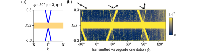
Appendix E Backscattering rate with initial waveguide at armchair orientation
In this section, we present the backscattering rate as a function of the energy and the transmission waveguide orientation for the fixed initial waveguide at the armchair orientation , see Fig. 11(b). We notice that the pattern is identical to Fig. 5 of the main text, except that there is an additional edge-band gap near zero energy due to the fixed initial waveguide, cf Fig. 11(a).