May
FPGA Random Number Generator
Abstract
Random number generation is a key technology that is useful in a variety of ways. Random numbers are often used to generate keys for data encryption. Random numbers generated at a sufficiently long length can encrypt sensitive data and make it difficult for another computer or person to decrypt the data. Other uses for random numbers include statistical sampling, search/sort algorithms, gaming, and gambling. Due to the wide array of applications for random numbers, it would be useful to create a method of generating random numbers reliably directly in hardware to generate a ready supply of a random number for whatever the end application may be. This paper offers a proof-of-concept for creating a verilog-based hardware design that utilizes random measurement and scrambling algorithms to generate 32-bit random synchronously with a single clock cycle on a field-programmable-gate-array(FPGA).
May 4th, 2022
FPGA, Verilog, Random Numbers, RNG, VHDL, Computer Architecture.
1 Introduction
Due to the extensive applications of random number generators, there is a need for processors to be able to provide this capability in a wide variety of applications. It would be useful to create a common logical design that could be dropped into existing computers to supply random numbers quickly and efficiently. The goal of this project aims to create a hardware implementation of a random number generator on a FPGA and demonstrate the randomness of the generated numbers.
1.1 Relevance to computer Architecture
The key topics that are covered in this project that are related to computer architecture are as followed.
1.1.1 Algorithm Implementation on hardware
One of the key skills in computer architecture is translating a mathematical algorithm into concrete hardware functions. This is done by using the many computer arithmetic functions such as multiplication, division, addition, shifts, gates, counters, AND/OR/XOR/NOT and other logical gates. These functions will have to be used combinationally to embody a mathematical algorithm to generate random numbers via hardware.
1.1.2 Utilizing I/O inputs on an FPGA
In the case of generating true-random numbers, often an analog measurement must take place. This is a great opportunity to use the Nexys A7 development board and interface with the I/O to obtain such a measurement and route that input into the design and compute with it. I/O is the backbone of how every computer communicates with its end-user, so demonstrating communication with I/O devices to obtain inputs and compute an output is a useful skill that can be applied to many computing applications.
1.1.3 Finite State Machines
By using combinational logic, this project will result in a finite state machine that performs the predetermined action of generating random numbers. By observing the state over each iteration, data outputs can be analyzed and displayed in creative ways.
1.1.4 Linear feedback in computer design
Many random number generators utilize algorithms with some sort of linear feedback. Linear feedback is unique in that the input is a linear function of the previous state. This property in computer design will allow us the ability to create random number generators that produce a continuous stream of outputs synchronously with the clock.
2 Background
Random number generation is a key technology that is useful in a variety of ways. Random numbers are often used to generate keys for data encryption. Random numbers at a sufficiently long length can encrypt sensitive data and make it difficult for another computer or person to decrypt the data. Other uses for random numbers are statistical sampling, computer simulation, and search/sort algorithms, gaming, and even casino/gambling machines.
2.1 Types of Random Numbers
There is an important distinction when it comes to generating random numbers—random number generators fall under two sub-types: pseudo-random, or true-random.
2.1.1 Pseudo-random numbers
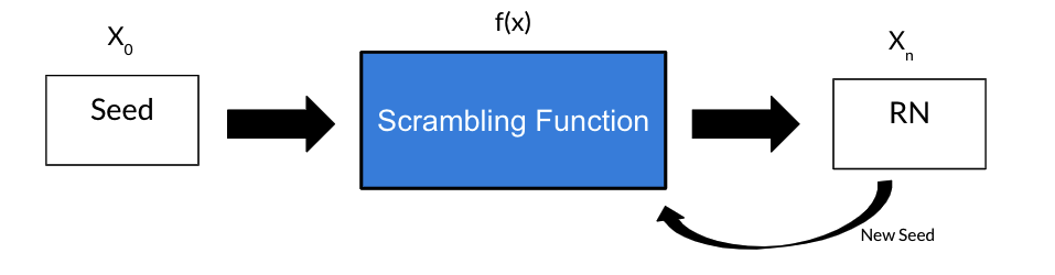
Pseudo-random numbers are generated via a mathematical algorithm and some starting value known as a “seed” to create a finite number of random numbers. The limit of these algorithms can be large, but after so many iterations repeating values are produced. Generating pseudo-random numbers happens entirely within a computer and can be generated in hardware/software without needing any external inputs.[1]
2.1.2 True-random numbers
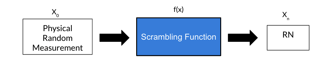
True-random numbers are considered truly random and are generated using a physical entity of randomness. This might be something like radioactive decay/entropy or electrical noise which are physically random events in the real world. Computers can take readings of these events via sampling, and produce a random number utilizing an algorithm to produce a random number.[1]
3 Technical Approach
The first step of demonstrating a solution to this challenge is to outline a system architecture block diagram that defines the function and flow of the individual components of the FPGA random number generator.
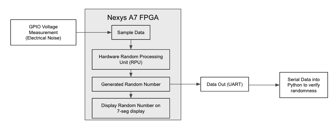
This design has several foundational blocks. First a voltage measurement must be taken utilizing the GPIO inputs on the Nexys A7 board. This will be acheived by sampling an analog voltage signal into a digital number via an analog-to-digital-converter (ADC). Then that voltage measurement will be fed into the random processing unit as a seed — which will be the scrambling functions that generates the random number of desired length. Next the random number is passed to two places: the 7 segment display of the Nexys A7 board, and to a UART transmit module which will send the random number to a connected computer. The connected computer will then use python to evaluate the numbers generated for statistical randomness.
3.1 Description of Work
The process to create the working design can be divided into 5 distinct functional modules.
-
1.
Verilog module that generates random numbers with specific algorithms.
-
2.
Verilog module that reads the Nexys A7 GPIO pins and prints to the segment display.
-
3.
Verilog module to send bytes of information over UART.
-
4.
Top-level verilog module that connects the previous modules for a standalone random number generator.
-
5.
Python module to read UART data and test for statistical randomness.
3.2 Random Algorithm Development Module
Two algorithms will be investigated simultaneously throughout this project as a method of generating the random numbers.
3.2.1 The Middle-Square Algorithm
The Middle-Square method, created by John Von Neumann, is an algorithm that takes an input number, then it squares the middle digits to get an output. That output is the next seed and the process continues in a linear feedback fashion.[2]
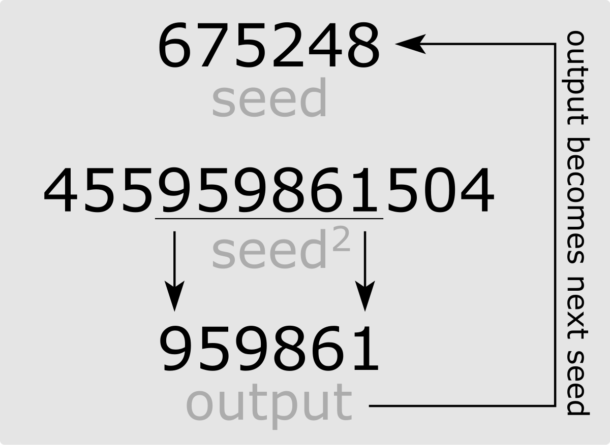
Implementing the middle square method is very simple in verilog. Since this design aims to produce 32-bit random numbers, a seed value that is 32-bits long must be taken as an input. Then the middle digits can be squared and produce the output as the next random number.
3.2.2 XORshift Algorithm
The XORshift method, created by George Marsaglia, is an extremely fast and efficient algorithm for generating random numbers. An XORshift algorithm works by taking the exclusive or (XOR) of a number with a shifted version of itself multiple times, before feeding back into the input again.[3]
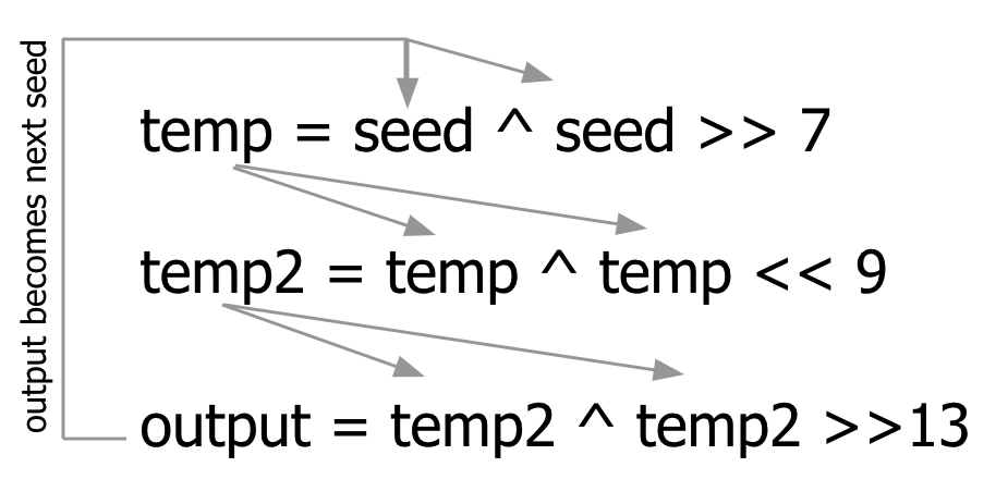
Much like implementing the middle-square method, the XORshift requires a seed value that is 32-bits long. It then performs a XOR with a shifted version of itself several times before outputting the random number.
3.2.3 Testbench for Random Algorithm Modules
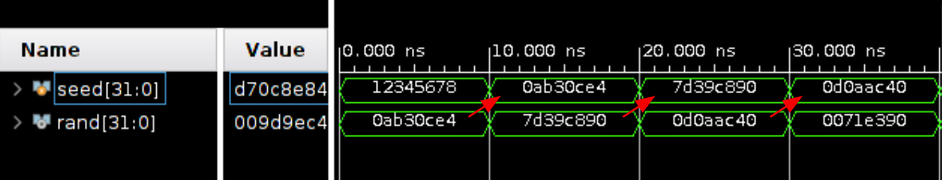
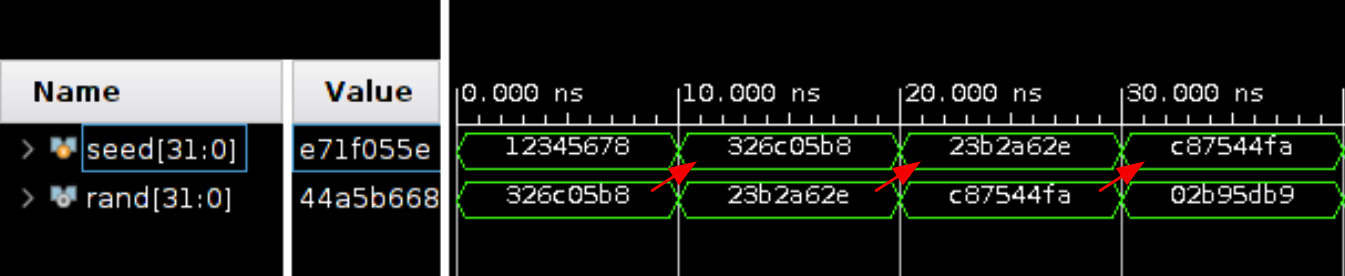
The next step is to test that both the Middle-Square and XORshift verilog modules are operating as intended. A verilog testbench can be used to setup a simple register and intialize a static starting seed, and then connect the output of the XORshift or Middle-Square to the seed input for subsequent iterations.
By using a manual input seed, a waveform output can be generated to verify that the algorithms are performing correctly over time. Note that the outputted random number is becoming the next seed input to each algorithm respectively.
3.3 Nexys A7 GPIO Read Module
The next module to will accomplish the task of reading a GPIO pin on the Nexys A7 development board for voltage and outputting the reading on the segment display.
3.3.1 Modify Board Constraints
The Nexys A7 development board files obtained directly from Digilent contain a constraint file titled ”Nexys-A7-100T-Master.xdc” which defines the mappings for physical pins into ports that are usable in the verilog design.[4] The digilent user guide has an in-depth walkthrough for how to setup the XADC, which is the on-board analog-to-digital converter linked to specific pins on the development board.
3.3.2 Instantiating the XADC and Segment Display
The XADC on the Nexys A7 is compatible with the Xilinx IP instantiation called XADC Wizard which is an easy to use wizard to configure the on-chip ADC of the FPGA.[5] It allows us to connect physical pins on the board as wires of data into the design. The ”do_out” signal is a 15-bit bus, however this particular ADC only provides 12-bits of precison to read each differential input pair in range of . These 12-bits will be converted to decimal values which will then be displayed on the segment display. The code for the seven segment display was used directly from Digilent’s github repository for the NexysA7 development example projects.[6]
3.3.3 Testing GPIO Module
The next step is to test that both the Nexys A7 board and verilog modules are correctly measuring voltage and displaying onto the segment display. To accomplish this, a simple voltage divider can be setup to use the 3.3V supply directly from the Nexys A7 board and divide the voltage to something in the range (below 1.0V). Following the formula for a two-resistor voltage divider, the following circuit is developed.
| (1) |
| (2) |
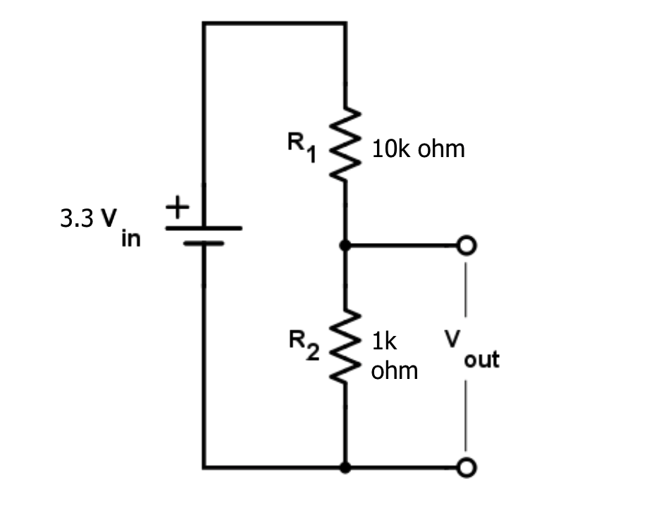
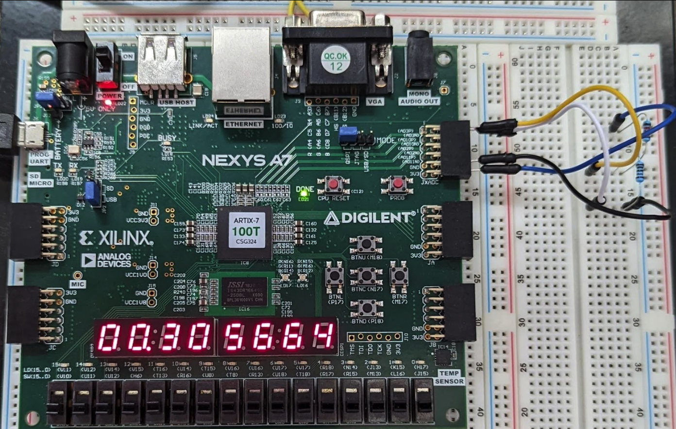
The results on the segment display indicate a reading of 0.3V which means that the verilog module successfully utilizes analog voltage inputs and converts them to digital data reliably. This will be important for measuring electrical noise as the input seed to the final random number generator.
3.4 UART Module
UART (universal asynchronous receiver-transmitter) is a communication protocol between devices that operates by sending bytes of information.[7] UART can be configured to work with serial protocols, which in the case of the Nexys A7 is Serial RS232 to USB transmitter/receiver via a dedicated FTDI™chip.[4]
3.4.1 Modify Board Constraints
The board constraints file ”Nexys-A7-100T-Master.xdc” must be modified again to enable the pins to the UART interface.
3.4.2 UART TX CTRL Module
Digilent’s github repository also provides a UART transmit VHDL (virtual hardware description language) code to use with the Nexys A7 Board.[6] VHLD is similar to verilog and can be used within the same design as long as the signals and connected nets are correctly configured.
To connect this module to a verilog design the following signals must be accounted for:
-
•
SEND: Triggers a send operation, set signal high for a single clock cycle to trigger a send. DATA must be valid when SEND is asserted. SEND should not be asserted unless READY is high.
-
•
DATA: 8 bits (1 byte). The UART code will add a stop bit to the final message.
-
•
CLK: 100 MHz system clock
-
•
READY: This signal goes low once a send operation starts, remains low until complete and ready to send next byte
-
•
UART_TX: Route this to the TX pin on the Nexys A7 (constraints .xcd file)
3.4.3 Verilog Logic to Send 4 Bytes
Since there are several signals that have to be asserted according to the UART transmit code, it means that there must be logic in the top-level verilog code to account for asserting signals and waiting for the READY signal before sending a byte of information. Since the goal is to generate 32-bit random numbers, this means that each number will need to be divided into 4 bytes. UART can only transmit one byte at a time, so each byte will need to be passed sequentially to get the entire random number transmitted.
3.4.4 Testing UART Module
The next step is to test that both the Nexys A7 board and verilog modules can correctly transmit a 32-bit number over the USB/RS232/UART interface. This can be setup by using a USB cable connected from the Nexys A7 board to a computer’s USB port. To set up serial communication, Python and the pySerial library make this process quick and easy.[8]
Now, the Nexys A7 board can be programmed with the UART module verilog code and connected to the computer running Python. The python program will begin the serial data communication and store the data into a text file.
The result of this test is the ”uart_byte” which was set to ”0x12345678” repeated 490,000 times and a text file 4.4MB in size. This means the FPGA can successfully transmit a 32-bit number continuously over UART to python which will be important later for analyzing the generated random numbers.
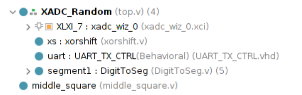
3.5 Top-level Verilog Design
Since there are now have three working modules—the random algorithm module, the GPIO module, and the UART module, the next step is to combine them into a single top level verilog design to generate random numbers. To accomplish this the physical jumper cables should be removed from the NexysA7 XADC pin headers so that the differential input pairs are reading ambient electrical noise. This is the event that is truly random that will be measured to use as the input seed into the random number algorithms. Once that is connected, the random number can be sent to the segment display as well as the UART transmit code to send each random number generated over serial for further analysis.
The verilog module hierarchy is as shown:
3.5.1 Testing Top-Level Verilog Design
The next step is to test that the top-level design is behaving as anticipated. It should now be generating a new 32-bit random number every clock cycle, printing numbers to the segment display, and transmitting the numbers over the UART interface to python. Since the GPIO module is providing electrical noise as the input seed to the random algorithms, they will continue to generate random numbers continuously and be refreshed with a new seed every 1000 clock cycles.
The python program will begin the serial data communication and store the data into a text file.
The result of this test is a text file filled with 490,000 randomly generated numbers represented in hexadecimal format. This means the system can successfully transmit a 32-bit random numbers over UART to python which can now be analyzed for statistical randomness.
3.6 Python Module
The final module is a python program to analyze the statistical randomness of the generated random numbers. The following program opens the text file filled with randomly generated numbers, then it iterates over the list of numbers and normalizes each number to be less than 1.0 converting each one to a float. If the set of random numbers is truly random, then the distribution of those numbers between 0 and 1 should be uniform. To demonstrate this in a clear way, each number will be evaluated. If the number is less than 0.5, then a single pixel on a blank canvas will be colored black. If the number is greater than 0.5, then a single pixel on the same canvas will be colored white. This process repeats for all 490,000 numbers until a 700 by 700 pixel image is created to represent the statistical randomness of the numbers.
3.7 Testing the Python Statistical Randomness Program
To test this final module, we can feed in a list of numbers that are generated with a pseudo-random number generator first. We can use the middle-square method from before, but instead of feeding in a seed from our XADC reading, we will set it to something static like 0x19238433. Recall that the middle-method will take this seed and square the middle digits making that the output, and the next iteration’s seed.


Some observations to note about this output right now is that it looks something like television static. What is being shown is the overal distribution of numbers greater than or less than 0.5 respectively where each pixel colored is one case or the other. While the result in Figure 25(a) may appear random at first glance, if you look (or move your eyes a bit further from this image), you might see there are several diagonal lines or patterns that start to appear. What this means at a high level is that the distribution of random numbers is actually repeated after some amount of time. That is why you can see a pattern in the distribution after some amount of time.
Figure 25(b) shows a unique case where the result is a feedback loop. Recall that the middle-square method takes the middle digits and squares them for the next input. What happens in the case where the middle digits are all zero? Since the algorithm ends up in a loop that will produce the number 0 forever. Since both of these tests were Pseudo-random numbers, it is expected that they cannot produce truly random numbers forever, so this result is to be expected.
4 Results
The final step of this project is to analyze the data from the random numbers generated by the Nexys A7 board using the GPIO measurement of ambient electrical noise as the input see to the random number algorithms.


Some observations to note about the final outcome. Figure 26(a) shows a picture resembling random television static, only this time there are no discernible lines or patterns in the output when compared to Figure 25(a). This is great news because it means that at a high-level it can be said with confidence that this method does not generate random numbers in a repeated pattern in any statistically significant way. The overall color of the image is gray meaning that it is likely that 50% of the numbers are greater than 0.5 and the remaining 50% are less than 0.5. This supports the idea that the numbers are truly random since there are no patterns and the distribution is uniform.
Observing Figure 26(b) one can see that it is much darker than the XORshift outcome. What this means is that this method tends to generate numbers that are overall smaller over time. While there is no discernible pattern, the fact that the distribution of these random numbers tends to be biased towards smaller numbers makes this method not truly random for generating all numbers possible with equal probability. This might be due to the fact that there are many 32-bit numbers where the middle 16bits can equal zero. In-fact, if this is the case at any point during the loop, the middle-square method will enter that feedback cycle of generating zero until a new seed is refreshed every 1000 clock cycles. This is likely the case.
Overall if one is looking for true random numbers, the most promising method looks to be the XORshift method presented.
4.1 Design Limitations
One limitation of this design and project is related to UART transmission. The design itself generates a new random number each clock cycle, however UART is only able to transmit the 4-bytes for each number at a limited baud rate of 115200 symbols per second. At a clock rate of 100MHz it turns out that the Nexys board can only transmit an entire 32-bit number over the UART interface once every 3500 clock cycles. This ultimately means that the analyzed random numbers are only getting a sample of the generated numbers once every 3500 generated numbers. Ideally, it would be best to analyze every single number generated by ensuring we either store the data or can transmit synchronously with the clock. However, the graphical outputs produced as a result of this project can still be valid since a statistical sample of a random set should still remain random.
5 Conclusions
This project proved several things:
-
•
Randomizing algorithms can be implemented directly in hardware using simple logical gates
-
•
Linear feedback-type machines are possible to create continuous operations where the output of one function is the next iteration’s input
-
•
XADC I/O support was added to the Nexys A7 board with the ability to read voltages accurately
-
•
A functioning UART interface over USB/RS232 serial from the Nexys A7 can be used to transmit data from the FPGA directly to another computer
-
•
Randomness of the generated numbers can be verified by graphically plotting the distribution
-
•
The XORshift method seems to be superior to the Middle-square method for generating random numbers
6 Future Recommendations
As mentioned in Section 4.1, UART transmission proved to be a bottle neck in retrieving and analyzing all random numbers generated by the Nexys A7 board. Some recommendations for improving this project or developing further could be:
-
1.
Instead of UART transmission in real-time, one might store the random numbers in a memory location on the FPGA first. Then use UART to iterate over each memory location an send all bytes of information without losing any to delays associated with UART speed.
-
2.
This project is setup to be instantiated into other verilog modules. Since it produces 32-bit random numbers each clock cycle perhaps one could implement this in MIPS and use the random number to do tasks like ”store word”, ”load word”, use the random numbers in arithemtic instructions, or perhaps to create a routine to fetch addresses randomly.
References
- [1] P. L’Ecuyer and U. Montreal, “History of uniform random number generation,” 11 2017.
- [2] J. von Neumann, “Various techniques used in connection with random digits,” in Monte Carlo Method, ser. National Bureau of Standards Applied Mathematics Series, A. S. Householder, G. E. Forsythe, and H. H. Germond, Eds. Washington, DC: US Government Printing Office, 1951, vol. 12, ch. 13, pp. 36–38.
- [3] G. Marsaglia, “Xorshift rngs,” Journal of Statistical Software, vol. 8, no. 14, p. 1–6, 2003. [Online]. Available: https://www.jstatsoft.org/index.php/jss/article/view/v008i14
- [4] “Nexys a7™ fpga board reference manual,” 2019. [Online]. Available: https://digilent.com/reference/learn/programmable-logic/tutorials/nexys-4-xadc-demo/start
- [5] “Xadc wizard,” 2022. [Online]. Available: https://www.xilinx.com/products/intellectual-property/xadc-wizard.html
- [6] Digilent, “Nexys a7 hardware repository,” https://github.com/Digilent/Nexys-A7-HW, 2020.
- [7] E. Pena and M. Legaspi, “Uart: A hardware communication protocol understanding universal asynchronous reciever/transmitter.”
- [8] C. Liechti, “pyserial,” https://github.com/pyserial/pyserial, 2021.