Gapless states and current control in strongly distorted gated trilayer graphene
Abstract
We investigate gated trilayer graphene partially devoid of outer layers and forming a system of two trilayers connected by a single layer of graphene. A difference in the stacking order of trilayers leads to the appearance of gapless states, one of which is mainly localized in the single graphene layer. We demonstrate that by changing the value of the gate voltage applied to the outer layers one can change the slope of of this state. As a consequence the direction of current flowing in the single layer graphene can also be changed, the effect that could be useful in practical applications.
I Introduction
There are several reasons for the high interest in multilayer graphene. One of them is the possibility of opening a tunable energy gap in gated multilayers with the Bernal-stacked arrangement of layers, which is important for electronic applications of graphene Ohta_2006 ; Castro_2007 ; Oostinga_2008 ; Zhang_Nature_2009 ; Szafranek_2010 ; Padilha_2011 ; Schwierz_2010 ; Lin_2008 ; Choi_2010 ; Santos_2012 ; Zhang_transistor_2018 . Multilayers focus also attention due to the emergence of flat bands and superconductive properties discovered for systems with twisted layers Jarillo2018 ; Chen_Nature_2019 ; Chittari_PRL_2019 ; Yin_PRB_2020 ; Liu_Nature_2020 ; Shen_Nat_Phys_2020 . Vacancies, adatoms and topological defects in multilayers are also investigated because they can induce magnetic moments important for spintronic applications An_SN_2018 ; Kishimoto_2016 ; Menezes_JPB_2015 ; Jaskolski_2016 ; Jaskolski_RSC_2019 ; Yazyev_RPP_2010 ; Nair_NC_2013 . Of particular interest are multilayers with domain walls that separate regions of different stacking order, due to the appearance of valley-protected gap states of topological character Wu_ACS_Nano_2015 ; Yin_NC_2016 ; Kazemi_APL_2013 ; Anderson_PRB_2022 ; Vaezi_2013 ; Alden_2013 ; San_Jose_2014 ; Pelc_2015 ; Jaskolski_2020 . Two gap states appear in gated bilayer graphene (BLG) when the stacking order changes from AB to BA, and three such states occur in the energy gap of gated trilayer graphene (TLG) at stacking domain wall ABC/CBA.
Recently it has been shown that strong deformation of gated bilayer and trilayer graphene with stacking domain walls, caused by partial removal of one of the layers, does not destroy their basic electronic properties, in particular topologically protected states in the energy gap Jaskolski_2019 ; Jaskolski_2021 . Here we investigate trilayer graphene partially peeled off the outer layers and thus forming a system of two trilayers connected by a single layer of graphene (SLG). Positive and negative voltages are applied to outer layers. When the trilayers differ in the stacking arrangement (ABC and CBA), valley-protected gapless states are still present in the energy gap although their number depends on the gate voltage . Some of these states localize almost exclusively in the region of single graphene layer providing one-dimensional currents in this layer. Most importantly, by changing the value of the slope of ) of the gapless state central to the energy cone also changes. In practice, this means the change of the direction of current that flows in the SLG, the effect that could be exploited in nanoelectronic devices based on multilayer graphene.
II System investigated and method of calculation
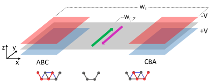
The investigated system is schematically shown in Fig. 1. It consists of two trilayers connected by a single graphene layer, i.e., TLG/SLG/TLG. The width of the central single layer is , measured as the number of four-atom unit cells along the (armchair) direction. It means that the TLGs are separated by about 3 nm. The system is infinite in both, the armchair and the zigzag directions, but is periodic only in the zigzag direction. The stacking order of layers in the left and right TLGs is ABC and CBA, respectively.
We work in the -electron tight binding approximation. Intra-layer and inter-layer hopping parameters eV and eV are used, respectively Castro_2007 ; Ohta_2006 . Voltages and are applied to the top and bottom layers, respectively. This keeps the Fermi level at zero energy. We consider two values of , 0.1 eV and 0.5 eV, because the layer localization of gapless states in multilayers with stacking domain walls depends on the value of vs Jaskolski_2018 ; Jaskolski_2020 . Surface Green function matching technique (SGFM) for three-terminal device (TLG/SLG/TLG) is used to calculate the local density of states (LDOS) Nardelli_1999 .
Since the system is periodic in the zigzag direction the LDOS is -dependent, where is the wave-vector corresponding to this periodicity. The LDOS is calculated in two regions: (i) in the entire structure shown in Fig. 1 of the width and (ii) in the very central part of SLG of the width . It has to be emphasized that although the LDOS is computed for finite segments of the widths and , the calculation within the SGFM takes into account the structure that extends to infinity on the left and right sides. To determine the localization of the gapless states we calculate also layer-resolved density distribution for individual states at the Fermi level i.e., in the center of the energy gap.
It is worth noting that because both outer layers are torn into two well-separated parts we cannot clearly indicate the position of the domain wall, as is the case when some layers are stretched, folded, delaminated or with a defect line Pelc_2015 ; Ju_Nature_2015 ; Lin_NL_2013 ; Peeters_PRB_2018 ; Jaskolski_2021 . Moreover, the zigzag edges of the half-planes of outer layers introduce zigzag-edge states that are expected to influence the energy spectrum of the investigated system.
III Results and discussion
First, let us recall that the energy spectrum of undisturbed, gated TLG with ABC/CBA stacking domain wall presents an energy gap and a triplet of gap states that connect the valence (VB) and conduction (CB) band continua Jaskolski_2020 . The slope of of all gap states is the same and for a given valley and is uniquely determined by the gate polarization Jaskolski_2018 . As demonstrated in Ref. Jaskolski_2021 one state of this triplet localizes mainly in the lower layer, another one in the upper layer and the third one in both outer layers with an admixture in the middle layer.
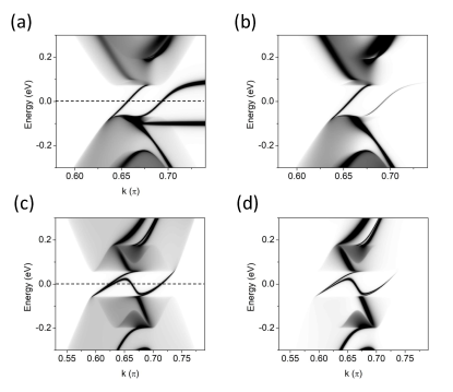
We start description of the results with the case . In Fig. 2 (a) the LDOS calculated for the region of width is shown. Although the TLG is severely perturbed, i.e., strips of width are removed from outer layers and no stacking domain wall can be clearly identified, one state linking VB and CB still persists. For and i.e., close to the cone center, this state is localized mainly in the SLG, what is confirmed in Fig 3 (a), where its layer-resolved density distribution is presented. Two zigzag edge states are seen for nota_zigzag_sublat . The one at eV is due to the zigzag edges of the upper half-planes of graphene nota_zigzag_degener . The zigzag-edge state at eV, which is due to the zigzag edges of the lower half-planes, couples strongly to another gap state, which starts at the top of the valence band. It has been checked that for this state localizes mainly in the lower layer and its component in the middle layer is negligible
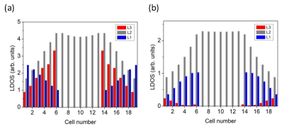
Fig. 2 (b) shows LDOS calculated in the central part of SLG of width (see Fig. 1). The most striking effect is strong resemblance of this energy spectrum to the LDOS of the entire structure of width , although the TLGs are distant from the region of SLG. It means that the energy spectrum of the TLGs is induced in the single layer of graphene. Consequently, it also means that the use of a single layer may be sufficient to take advantage of the properties of the entire system.
The zigzag-edge state at eV is not seen because the sublattice of the upper layer at which this state localizes is decoupled from the middle layer. The zigzag-edge state at eV is only weakly represented, since its sublattice in the upper layer is weakly coupled (by ) to the middle layer.
The energy spectrum of the investigated system for eV is shown in Fig. 2 (c) nota_z_05 . For this gate voltage, three gapless states are maintained, although they differ significantly from the triplet of gap states that occur in the case of TLG with ABC/CBA stacking domain wall Jaskolski_2021 . Here, the middle gap state changes twice the slope of . To see better this effect the magnification of the energy spectrum close to is presented in Fig. 4 (b). We have checked that the left and right gap states are localized almost exclusively in the outer layers. However, the middle gap state, similarly to the gap state of the case, localizes mainly in the middle layer, as shown in Fig. 3 (b). There is a certain correspondence between these two states: both cross the Fermi level at (i.e. at the cone center) and both localize in the middle layer.
The LDOS calculated in the central part of SLG is presented in Fig. 2 (d). Similar to eV, also this time the energy spectrum of the entire system is, to a large extent, induced in the single graphene layer. The topological gap states are well seen and the band continua are also partially preserved.
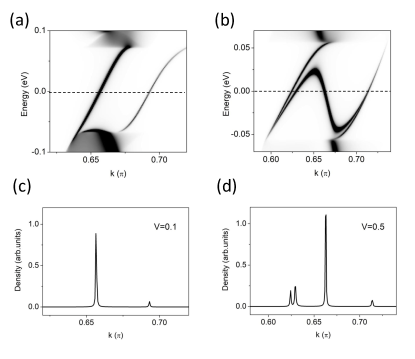
Magnification of the LDOS close to the cone center, calculated in the central part of the SLG, for eV and eV are presented in Fig. 4 (a) and (b), respectively. The LDOS calculated at is presented in Figs. 4 (c) and (d). This figure shows that the main contribution to charge density at comes from the states that cross at .
These gap states can curry one dimensional currents along the zigzag direction, localized in the SLG. For in the adjacent valley, i.e., , all the gap states have reversed slopes due to time-reversal symmetry, so the currents are valley-polarized. This property was proposed long ago to use as valley filter and valley valve Martin_PRL_2008 in valleytronics Rycerz_2007 ; Kundu_2016 . Polarization of valley currents can be changed by the reversal of the gate voltage Jaskolski_2016 . Here we demonstrate that for the system under study also the slope of of the gap state at and changes with the change of magnitude of . Therefore, we gain the possibility of changing the direction of valley current in this state by changing only the value of the gate voltage, what in Fig. 1 is illustrated by green and pink arrows.
IV Conclusions
We have studied gated trilayer graphene, strongly distorted by removal of wide strips of the outer layers. The resulting system consists of two trilayers of different stacking order, ABC and CBA, connected by single graphene layer. We have investigated the energy spectrum of the entire TLG/SLG/TLG and the local density of states in the center of SLG. The calculations have been performed for two values, 0.1 eV and 0.5 eV, of the gate voltage applied to outer layers of TLGs.
The ABC/CBA stacking domain wall in gated trilayer graphene causes the emergence of three topologically protected states in the energy gap. Our calculations show that when such a trilayer is strongly deformed and reduced to the TLG/SLG/TLG system, some gapless state still exist, and their number depends on the gate voltage. When is smaller than the interlayer coupling , only one gap state connects the valence and conduction band continua, while for three gapless states persists. In the latter case, the dispersion of the middle gap state changes twice its slope. Therefore, the sign of the slope of of the gap state at the Fermi Energy and at the cone center changes when the value of is changed. As a consequence, the sign of the velocity of electrons occupying this state, and thus the direction of the corresponding current, also changes, the effect that potentially could be exploited in nanoelectronic applications based on graphene.
Additionally, we have demonstrated that the enrgy spectrum of SLG is almost the same as the spectrum of the entire system (except the zigzag-edge states). Moreover, the gap state that at changes its velocity when changes its value from 0.1 eV to 0.5 eV is localized almost exclusively in this single layer, although it emerges because the adjacent trilayers have different stacking order. Consequently, the one-dimensional current related to this state flows mainly in the single graphene layer. We can conclude that the physics of the trilayer system is still present in the single graphene layer when this system is partially stripped of the outer layers.
References
- [1] T. Ohta, A. Bostwick, T. Seyller, K. Horn, and E. Rotenberg, Science 313, 951 (2006).
- [2] E. V. Castro, K. S. Novoselov, S. V. Morozov, N. M. R. Peres, J. M. B. L. dos Santos, J. Nilsson, F. Guinea, A. K. Geim, and A. H. C. Neto, Phys. Rev. Lett. 99, 216802 (2007).
- [3] J. B. Oostinga, H. B. Heersche, X. Liu, A. F. Marpurgo, and L. M. K. Vandersypen, Nat. Mater. 7, 151 (2008).
- [4] Y. Zhang, T.-T. Tang, C. Girit, Z. Hao, M. C. Martin, A. Zettl, M. F. Crommie, Y. R. Shen, and F. Wang, Nature (London) 459, 820 (2009).
- [5] B. N. Szafranek, D. Schall, M. Otto, D. Neumaier, and H. Kurz, App. Phys. Lett. 96, 112103 (2010).
- [6] J. E. Padilha, M. P. Lima, A. J. R. da Silva, and A. Fazzio, Phys. Rev. B 84, 113412 (2011).
- [7] F. Schwierz, Nat. Nanotechnol. 5, 487 (2010).
- [8] Y.-M. Lin and P. Avouris, Nano Lett. 8, 2119 (2008).
- [9] S.-M. Choi, S.-H.Jhi, and Y.-W. Son, Nano Lett. 10, 3486 (2010).
- [10] H. Santos, A. Ayuela, L. Chico, and E. Artacho, Phys. Rev. B 85, 245430 (2012).
- [11] Q. Zhang, Y. Yaofeng, K. S. Chan, Z. Mu, and J. Li, App. Phys. Express 1, 075104 (2018).
- [12] Y. Cao, V. Fatemi, S. Fang, K. Watanabe, T. Taniguchi, E. Kaxiras, and P. Jarillo-Herrero, Nature 556, 43 (2018).
- [13] E. Chen, A. L. Sharpe, P. Gallagher, I. T. Rosen, E. J. Fox, L. Jiang, B. Lyou, H. Li, K. Watanabe, T. Taniguchi, J. Jung, Z. Shi, D. Goldhaber-Gordon, Y. Zhang, and F. Weng, Nature 572, 215 (2019).
- [14] B. L. Chittari, G. Chen, Y. Zhang, F. Wang, and J. Jung, Phys. Rev. Lett. 122, 016401 (2019).
- [15] L.-J. Yin, L.-Z. Yang, L. Zhang, Q. Wu, X. Fu, L.-H. Tong, G. Yang, Y. Tian, L. Zhang, and Z. Qin, Phys. Rev. B 102, 241403(R) (2020).
- [16] X. Liu, Z. Hao, E. Khalaf, J. Y. Lee, Y. Ronen, H. Yoo, D. H. Najafabadi, K. Watanabe, T. Taniguchi, A. Vishwanath, and P. Kim, Nature 583, 221 (2020).
- [17] Ch. Shen, Y. Chu, Q. Wu, N. Li, S. Wang, Y. Zhao, J. Tang, J. Liu, J. Tian,K. Watanabe, T. Taniguchi, R. Yang, Z. Y. Meng, D. Shi, O. V. Yazyev, and G. Zhang, Nat. Phys. 16, 520 (2020).
- [18] M. An, Q. Deng, Y. Li, H. Song, and M. Su, Superlattices Microstructures 123, 172 (2018).
- [19] K. Kishimoto and S. Okada, Jap. J. Appl. Phys., 55, 06GF06 (2016).
- [20] M.G. Menezes and R. B. Capaz, J. Phys. Condens. Matter 27, 335302 (2015).
- [21] W. Jaskolski, M. Pelc, L. Chico, and A. Ayuela, Nanoscale 8, 6079 (2016).
- [22] W. Jaskolski and A. Ayuela, RSC Adv. 9, 42140 (2019).
- [23] O. V. Yazyev, Rep. Prog. Phys. 73, 056501 (2010).
- [24] R. R. Nair, I.-L. Tsai, M. Sepioni, J. Keinonen, A. V. Krasheninnikov, A. H. Castro-Neto, M. I. Katsnelson, A. K. Geim, and I. V. Grigorieva, Nat. Commun. 4, 1 (2013).
- [25] H.-Ch. Wu, A. N. Chaika, T.-W. Huang, A. Syrlybekov, M. Abid, V. Y. Aristov, O. V. Molodsova, S. V. Babenkov, D. Marchenko, J. Sanchez-Barriga, P. S. Mandal, A. Y. Varykhalov, Y. Niu, B. E. Murphy, S. A. Krasnikov, O. Lubben, J. J. Wang, H. Liu, L. Yang, H. Zhang, M. Abid, Y. T. Janabi, S. N. Molotkov, Ch.-R. Chang, and I. Shvets, ACS Nano 9 8967 (2015).
- [26] L.-J. Yin, H. Jiang, J.-B. Qiao, and L. He, Nat. Commun. 7, 11760 (2016).
- [27] A. S. Kazemi, S. Crampin, and A. Ilie, Appl. Phys. Lett. 102, 163111 (2013).
- [28] P. Anderson, Y. Huang, Y. Fan, S. Qubbaj, S. Coh, Q. Zhou, and C. Ojeda-Aristizabal, Phys. Rev. B 105, L081408 (2022).
- [29] A. Vaezi, Y. Liang, D. H. Ngai, L. Yang, and E.-A. Kim, Phys. Rev. X 3, 021018 (2013).
- [30] J. S. Alden, A. W. Tsen, P. Y. Huang, R. Hovden, L. Brown, J. Park, D. A. Muller, and P. L McEuen, Proc. Natl. Acad. Sci. 110, 11256 (2013).
- [31] P. San-Jose, R. V. Gorbachev, A. K. Geim, K. S. Novoselov, and F. Guinea, Nano Lett. 14, 2052 (2014).
- [32] M. Pelc, W. Jaskolski, A. Ayuela, and L. Chico, Phys. Rev. B 92, 085433 (2015).
- [33] W. Jaskolski and G. Sarbicki, Phys. Rev. B 102, 035424 (2020).
- [34] W. Jaskolski, Phys. Rev. B 100, 035436 (2019).
- [35] W. Jaskolski, Mol. Phys., e2013554, doi.org/10.1080/00268976.2021.2013554.
- [36] W. Jaskolski, M. Pelc, G. W. Bryant, L. Chico, and A. Ayuela, 2D Materials 5, 025006 (2018).
- [37] M. B. Nardelli, Phys. Reb. B 60, 7828 (1999).
- [38] L. Ju, Z. Shi, N. Nair, Y. Lv, C. Jin, J. Velasco, Jr., C. Ojeda-Aristizabal, H. A. Bechtel, M. C. Martin, A. Zettl, J. Analytis, and F. Wang, Nature (London) 520, 650 (2015).
- [39] J. Lin, W. Fang, W. Zhou, A. R. Lupini, J. C. Idrobo, J. Kong, S. J. Pennycook, and S. T. Pantelides, Nano Lett. 13, 3262 (2013).
- [40] T. L. M. Lane, M. Andelkovic, J. R. Wallbank, L. Covaci, F. M. Peeters, and V. I. Falko, Phys. Rev. B 97, 045301 (2018).
- [41] M. Fujita, K. Wakabayashi, and K, Kusakabe, J. Phys. Soc. Jpn. 65, 1920 (1996).
- [42] K. Nakada, M. Fujita, G. Dresselhaus, and M. S. Dresselhause, Phys. Rev. B 54, 17954 (1996).
- [43] W. Jaskolski, A. Ayuela, M. Pelc, H. Santos, and L. Chico, Phys. Rev. B 83, 235424 (2011).
- [44] Zigzag edge states occur in the case of graphene half-planes (or graphene nanoribbons) with zigzag edges. They have the shape of flat bands beginning at the cone () and ending at . The corresponding wave functions are localized at the sublattice defined by the outermost edge atoms Wakabayashi ; Nakada ; Jaskolski_2011 .
- [45] Since for each of the outer layers there are two graphene half-planes, the zigzag edge states are doubly degenerate.
- [46] Here, the zigzag edge states are at eV. They do not couple to the gap states, since they are energetically well separated from the gap.
- [47] I. Martin, Y. M. Blanter, and A. F. Morpurgo, Phys. Rev. Lett. 100, 036804 (2008).
- [48] A. Rycerz, J. Tworzydlo, and C. W. Beenakker, Nat. Phys. 3, 172 (2007).
- [49] A. Kundu, H. A. Fertig, and B. Seradjeh, Phys. Rev. Lett. 116, 016802 (2016).