Compound Defects in Halide Perovskites:
A First-Principles Study of CsPbI3
Abstract
Lattice defects affect the long-term stability of halide perovskite solar cells. Whereas simple point defects, i.e., atomic interstitials and vacancies, have been studied in great detail, here we focus on compound defects that are more likely to form under crystal growth conditions, such as compound vacancies or interstitials, and antisites. We identify the most prominent defects in the archetype inorganic perovskite CsPbI3, through first-principles density functional theory (DFT) calculations. We find that under equilibrium conditions at room temperature, the antisite of Pb substituting Cs forms in a concentration comparable to those of the most prominent point defects, whereas the other compound defects are negligible. However, under nonequilibrium thermal and operating conditions, other complexes also become as important as the point defects. Those are the Cs substituting Pb antisite, and, to a lesser extent, the compound vacancies of PbI2 or CsPbI3 units, and the I substituting Cs antisite. These compound defects only lead to shallow or inactive charge carrier traps, which testifies to the electronic stability of the halide perovskites. Under operating conditions with a quasi Fermi level very close to the valence band, deeper traps can develop.
keywords:
Compound defects, halide perovskites, recombination reaction, stability, first-principlesCenter for Computational Energy Research, Department of Applied Physics, Eindhoven University of Technology, P.O. Box 513, 5600MB Eindhoven, the Netherlands. \alsoaffiliationCenter for Computational Energy Research, Department of Applied Physics, Eindhoven University of Technology, P.O. Box 513, 5600MB Eindhoven, the Netherlands. \alsoaffiliationCenter for Computational Energy Research, Department of Applied Physics, Eindhoven University of Technology, P.O. Box 513, 5600MB Eindhoven, the Netherlands. \alsoaffiliationCenter for Computational Energy Research, Department of Applied Physics, Eindhoven University of Technology, P.O. Box 513, 5600MB Eindhoven, the Netherlands. \alsoaffiliationComputational Materials Science, Faculty of Science and Technology and MESA+ Institute for Nanotechnology, University of Twente, P.O. Box 217, 7500AE Enschede, the Netherlands.
![[Uncaptioned image]](/html/2209.03484/assets/TOC_image/TOC.png)
1 Introduction
On the basis of their outstanding efficiency (25.7% to date 1) and relative ease of fabrication, halide perovskite solar cells seem to be poised for large scale applications. The primary obstacle blocking their present commercialization is their relative rapid degradation under operating conditions 2, 3, 4, 5. On a microscopic level, lattice defects in the perovskite materials initiate the degradation process, as they facilitate migration of ions 6, 7, 8, 9, 10, chemical reactions 11, 12, phase transitions 13, and phase segregation 14.
Because of the experimental difficulties in characterizing defect structures microscopically, much of our current understanding of lattice defects in halide perovskites stems from results obtained from electronic structure calculations based on density functional theory (DFT). Following common semiconductor practice 15, 16, elementary defects consisting of single atomic interstitials, vacancies, or antisites have been at the center of interest 17, 18, 19, 20, 21. In a previous work 22, we have studied vacancy and interstitial point defects in six primary Pb- and Sn-based halide perovskites with different cations (Cs, MA, FA) and anions (I, Br, Cl), within a single computational framework 23. One prevalent conclusion from most of these computational studies is that in these materials the points defects with the highest concentrations under equilibrium growth conditions, only introduce shallow traps.
Defects in halide perovskites with a more complex structure have also been considered 24, 25, 26. Conceptually, such complex defects can be thought of as resulting from a recombination of simple atomic point defects (vacancies or interstitials) to, for instance, PbI2 or MAI compound vacancies in MAPbI3 25, 24, 26. Within this line of thought also antisites can be interpreted as compound defects, resulting from a recombination of an interstitial and a vacancy of different species. For instance, in CsPbI3, cation antisites result from a recombination of a Cs vacancy (interstitial) and an Pb interstitial (vacancy) 20. Some compound defects have been predicted to form shallow defects only 25, 20, whereas others have the potential to form deep traps 24, 27.
The formation energy of compound defects is typically much higher than that of simple point defects, which implies that under normal equilibrium conditions (room temperature, atmospheric pressure) the concentration of compound defects, including antisites, is negligible 15, 16, 17, 18. However, many crystal growth conditions are highly nonequilibrium, and defects can be formed during growth in appreciable concentrations 22. In molecular dynamics simulations that use a reactive force field 10, 28, applied to halide perovskites containing an appreciable amount of point defects, one often observes recombination of the latter to compound defects. From positron annihilation lifetime spectroscopy, assisted by DFT calculations, there is evidence of charge carrier trapping at compound vacancy defects in MAPbI3 26.
In this paper, we study compound defects, vacancies, interstitials and antisites, in the archetype inorganic perovskite CsPbI3 by means of first-principles DFT calculations. Not only do we calculate their equilibrium concentrations, but explicitly considering the possible recombination reactions of elementary point defects, we also assess their concentrations under nonequilibrium conditions. The effect of these compound defects on the electronic properties is examined, in particular their potential to form deep traps.
2 Computational Methods
2.1 DFT calculations
Density functional theory (DFT) calculations are performed with the Vienna Ab-Initio Simulation Package (VASP) 29, 30, 31, employing the SCAN+rVV10 32, 23 functional for electronic calculations and geometry optimization. Our calculations use a plane wave kinetic energy cutoff of 500 eV and a -point-only k-point mesh. The energy and force convergence criteria are set to 10-4 eV and 0.02 eV/Å, respectively. Spin-orbit coupling is omitted, as it has little effect on the formation energies of defects 23. Spin polarization is included in all calculations.
As in our previous work 22, point defects or compound defects are created in a orthorhombic supercell of CsPbI3, which contains 32 formula units. The lattice volume and ionic positions of the pristine supercell are fully relaxed. Within the supercell, atomic positions of defective structures are optimized. For antisite defects, we use the notation to indicate that atom substitutes atom in the lattice. We consider twelve different compound complexes, i.e., the three compound vacancies , , and , the two compound interstitials and , the six antisites , , , , , and , and the compound antisite .
2.2 Defect Formation Energy
Under equilibrium conditions, the concentrations of lattice defects can be obtained from Boltzmann statistics
| (1) |
where indicates the type of defect, either a simple interstitial or vacancy point defect, or a compound interstitial or vacancy, or an antisite defect, with charge ; is the defect concentration, and is the density of possible sites for that particular defect (including orientational degrees of freedom if the defect in not spherically symmetric), where usually ; is the defect formation energy (DFE), is the temperature, and is the Boltzmann constant.
Different types of defects have different charges, but if no external charges are injected, then as a whole a material has to be charge neutral
| (2) |
where and are the intrinsic charge densities of holes and electrons of the semiconductor material. The charge neutrality condition, Eq. (2), fixes the intrinsic Fermi level.
The DFE is calculated from the expression 15
| (3) | ||||
where and are the DFT total energies of the defective and pristine supercells, respectively, and and are the number of atoms and chemical potential of atomic species added to () or removed from () the pristine supercell in order to create the defect. We use the chemical potentials ; Cs,Pb,I, as determined for I-medium conditions in our previous work 22.
Creating a charge requires taking electrons from or adding them to a reservoir at a fixed Fermi level. The latter is calculated as , with , the band gap, and the energy of the valence band maximum. As it is difficult to determine the latter from a calculation on a defective cell, one establishes in the pristine cell, shifted by , which is calculated by lining up the core level on an atom in the pristine and the neutral defective cell that is far from the defect 15, 33. The supercell in the calculation and the dielectric screening in CsPbI3 are sufficiently large, so that the electrostatic interaction between a charged point defect and its periodically repeated images can be neglected 19, 23, 22. In addition, we neglect vibrational contributions to the DFEs, and the effect of thermal expansion on the DFEs, as these are typically small in the present compounds 23, 34.
2.3 Recombination Reaction
We model the recombination of point defects to a compound defect as a chemical reaction
| (4) |
Reaction equilibrium is defined by
| (5) |
with and the chemical potentials of species and , given by
| (6) | |||
| (7) |
where ; are the DFEs according to Eq. (3), , are concentrations, and , are the densities of possible sites (see Table S1 of the Supporting Information for details). Note that we do not assume that charge is conserved in reaction (4). The electron reservoir with Fermi energy can supply electrons or holes, which is accounted for in the DFEs. Equations (5)-(7) give the law of mass action
| (8) |
| (9) |
where is the reaction energy of reaction (4).
If all (simple and compound) defects are in equilibrium with reservoirs at chemical potentials , Eq. (3), then their concentrations are given by Eq. (1), and trivially obey the law of mass action, Eq. (8). Typically, however, point defects and compound defects are initially created at concentrations and , respectively, in a crystal growth process, after which the crystals are extracted and kept at room temperature. The defects then remain, but they can recombine according to Eq. (4). Not only does this include the possible formation of compound interstitials or vacancies, but also the formation of antisites through the recombination of an interstitial and a vacancy.
2.4 Charge State Transition Level
Under operating conditions, charges are injected in the material, shifting the positions of the (quasi) Fermi levels for electrons and holes. The charge state transition level (CSTL) is defined as the Fermi level position where the charge states and of the same type of defect have equal formation energy, . As the DFEs have a simple linear dependence on , Eq. (3), this condition can be expressed as
| (11) |
where is the DFE calculated at . The CSTLs are important for the electronic properties; if these levels are deep inside the band gap, they can trap charge carriers, and act as nonradiative recombination centers.
The band gap calculated with SCAN+rVV10 suffers from the DFT band gap error. However, we would argue that the positions of the CSTLs with respect to the band edges are correct, because the defects’ electronic states have a character similar to either the valence band or the conduction band 35. For a more detailed discussion, see Ref. 22.
3 Results and discussion
3.1 Equilibrium Conditions
Formation of compound defects in semiconductors is often driven by the attractive electrostatic interaction between defects with opposite charge states 15, 16. Possible compound vacancies in CsPbI3, resulting from recombination of the point vacancies , and , are then , and , where the neutral state indeed turns out to be the most stable charge state under intrinsic conditions. Optimized structures of these defects are shown in Figures 1(a-c).
Following the same reasoning, we find the neutral compound interstitial defects and , shown in Figures 1(d,e) through recombination of the point interstitials , , and . For larger potential compound interstitials, such as , we found that the lattice becomes too distorted and the DFE becomes very large.
Formation energies of the compound vacancies and interstitials, calculated according to Eq. (3), are shown in Figures 2(a,b). Taking into account of all point defects and compound defects, the intrinsic Fermi level, , calculated with the charge neutrality condition, Eq. (2), is 0.58 eV with respect to the VBM. At this condition and are the dominant atomic point defects 22, and the antisite , to be discussed below, is the most dominant compound defect. The compound vacancy and interstitial defects listed above, are then all stable in the neutral state. A list of the DFEs and concentrations, calculated at the intrinsic Fermi level, of these compound defects is given in Table 1.
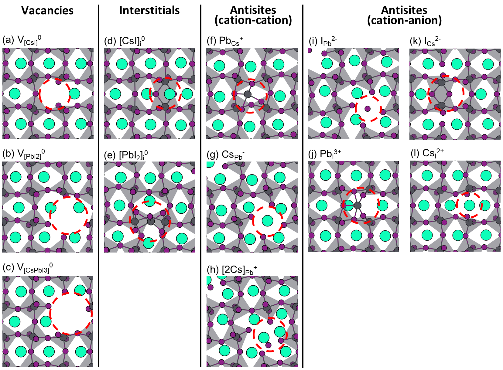
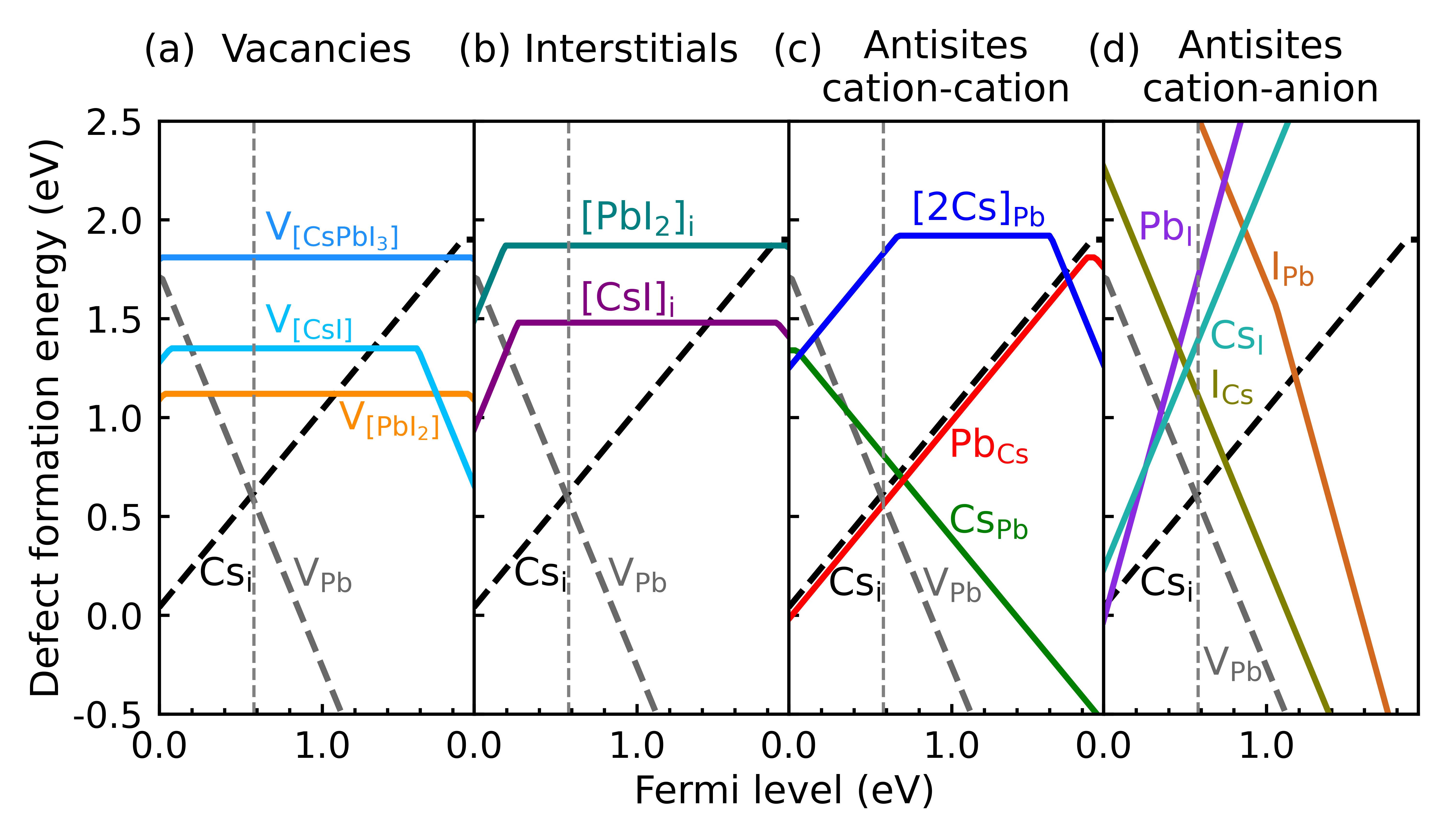
A compound vacancy defect creates a considerable hole in the lattice, see Figures 1(a-c), and its DFE is correspondingly high. The vacancy is relatively easiest to form, with a DFE of 1.12 eV, followed by and , whose DFEs are 1.35 eV and 1.81 eV, respectively. All of these numbers are eV higher than the DFEs of the simple point defects and , which means that concentration of compound vacancy defects is negligible at room temperature under equilibrium conditions (Table 1).
Compound interstitial defects, and , can be accommodated in the CsPbI3 lattice by a distortion or tilting of the Pb-I octahedra, see Figures 1(d,e), albeit at a considerable energy penalty, with DFEs of 1.48 eV and 1.87 eV, respectively. We conclude that compound interstitial defects also have negligible concentrations at room temperature under equilibrium conditions, see Table 1.
Turning to antisite defects, as there are two different cations in CsPbI3, antisites can be formed among cations, i.e., by a cation of one type occupying a position of a cation of the other type, (Pb substitutes Cs), or , see Figures 1(f, g). We stick to the nomenclature of antisites, but note that replacing one cation by another can lead to a notable local distortion of the lattice, such that the substituting ion is significantly displaced from the lattice position of the original ion. Pb ions are nominally 2+, and Cs ions are 1+, so it is not surprising to find the most stable charge states of these antisites as and . The DFE of is comparable to that of the simple point defects and , see Figure 2(c) and Table 1, which means that this antisite occurs relatively frequently under equilibrium conditions. The antisite defect has a DFE that is 0.25 eV larger than that of , making it less favorable.
| Defects | Reaction | ||||
| (eV) | (cm-3) | (eV) | (cm-3) | ||
| Vacancies | |||||
| 1.35 | |||||
| 1.12 | |||||
| 1.81 | |||||
| Interstitials | |||||
| 1.48 | 0.16 | ||||
| 1.87 | |||||
| Antisites (cation-cation) | |||||
| 0.56 | |||||
| 0.81 | |||||
| 1.83 | 0.01 | ||||
| Antisites (cation-anion) | |||||
| 2.51 | 1.24 | ||||
| 1.72 | 0.25 | ||||
| 1.10 | |||||
| 1.40 | 0.08 | ||||
a The specific nonequilibrium conditions are defined by defect formation at an elevated temperature equilibrium at K, followed by allowing for recombination through isolation at K.
In principle it is possible that a Pb vacancy, , captures two Cs+ ions to form the antisite, see Figure 1(h). Somewhat surprisingly, the most stable charge state at the intrinsic Fermi level of this antisite is . Its DFE is, however, eV larger than that of the antisite, demonstrating that it is difficult to plant two Cs ions in one Pb lattice position, see Figures 1(g) and (h).
A second possible type of antisite results from placing an anion on a cation position, or vice versa. There are four possibilities, see Figures 1(i-l). Again we maintain the nomenclature of antisites, but note that the replacing anion or cation typically does not occupy a lattice site. For instance, in the antisite the I ion does not replace the Cs ion at its lattice position, Figure 1(k). Instead, it forms a Pb-I-Pb bridge bond nearby, which is a typical bonding configuration for I interstitials 22. In this sense, an antisite is actually a bonding configuration between a vacancy and an interstitial.
The most stable charge states of these antisites can be guessed from summing the charges of the point defects that can recombine to these antisites. For instance, and antisites originate from recombining , respectively interstitials with vacancies, whereas the antisite results from recombining an interstitial with a vacancy. is an exception to this rule; it might be a recombination between an interstitial and a vacancy. In general, cation-anion antisites lead to unusually high charge states for the defects inserted into the CsPbI3 lattice, Figures 1 (i-l). This might in part explain their large DFEs, where all cation-anion antisite defects have a DFE that is at least eV larger than that of simple point defects, Figure 2 and Table 1.
In summary, under equilibrium conditions at room temperature, only the formation of cation(Cs)-cation(Pb) antisites is prominent, with presenting a comparable concentration to those of the dominant point defects and , and is formed to a lesser extent. Other compound defects, antisites, compound vacancies or interstitials, are not favorable due to their large DFEs.
3.2 Nonequilibrium Conditions
Defect concentrations can change drastically under nonequilibrium conditions. Highly nonequilibrium conditions typically occur during the growth of the perovskite crystals. The resulting concentration of defects can then not be simply deduced from the equilibrium relation, Eq. (1). The types and concentrations of defects that occur of course depend on the exact growth conditions. To estimate the potential role played by compound defects, we explore the following model.
It starts from the assumption that initially defects are created at an elevated temperature, which could reflect an annealing step during the growth process, for instance, with concentrations that can be estimated from Eq. (1). The crystal is then brought to room temperature, where the point defects and compound defects present are allowed to recombine or dissociate, according to Eq. (8), under the constraints of conservation of the total number of atoms in the defects, Eq. (10).
A key parameter determining the recombination reaction is the reaction energy, Eq. (9). Table 1 shows the reaction energies, calculated at the intrinsic Fermi level, of the recombination reactions that lead to the compound defects, and Figure 3(a) shows the reaction energies as a function of the Fermi level. For a recombination reaction to lead to an appreciable concentration of a compound defect, its reaction energy needs to be significantly negative.
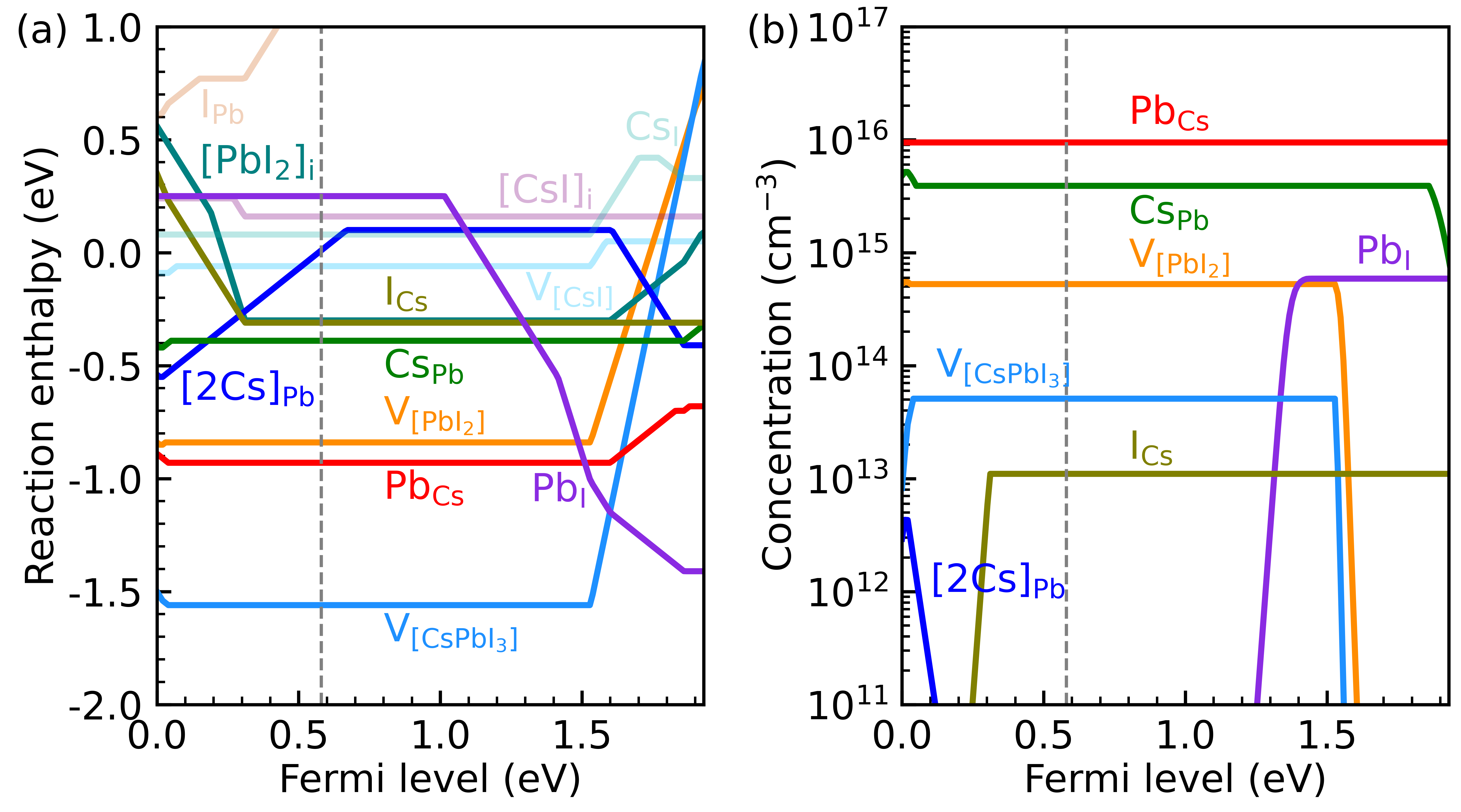
Figure 3(a) and Table 1 show that at the intrinsic Fermi level this is the case for the compound vacancies and and the antisite , with reaction energies in the range of to eV. The antisites and , as well as the compound interstitial have a moderately negative reaction energy between and eV, whereas that of the compound vacancy is marginally small. The reaction energies of other compound defects, anion-cation antisites (except the mentioned ) and the double antisite , or the compound interstitial , are positive, which means that these complexes are not formed in significant concentrations.
However, merely having a negative reaction energy does not imply that a compound defect will form in an appreciable concentration, as formation of a complex necessarily involves a decrease in entropy. Using the law of mass action, Eq. (8), which is based upon free energies, the effects of entropy are included. At room temperature equilibrium conditions, the most prominent point defects are the Pb vacancy and the Cs interstitial , with concentrations of cm-3, cm-3, respectively 22. Under those conditions, all compound defects have a concentration that is at least three orders of magnitude lower, see Figure S1 of the Supporting Information, which means that the loss of entropy involved in their formation reaction essentially prohibits the occurrence of compound defects. The antisite defect is an exception, which forms in a large concentration of cm-3 resulting from its low formation energy rather than the recombination of point defects.
At K the concentrations of the most prominent point defects, and , and the cation-cation antisite are raised to cm-3, see Figure S2 and Table S2 of the Supporting Information. Based on these initial conditions, the concentrations of compound defects at K (and intrinsic Fermi level, Eq. (2)), according to Eqs. (8) and (10), are shown in Figure 3(b). Most noticeable under these circumstances is that the two cation point defects recombine to form the antisite in a large concentration of cm-3.
A third relatively prominent defect is the compound vacancy with a concentration of cm-3. The compound vacancy and the anion-cation antisite occur at lower concentrations of cm-3 and cm-3, respectively, whereas the concentrations of the other compound defects are much smaller (under intrinsic Fermi level conditions).
In summary, whereas at equilibrium conditions compound defects are unlikely to form at room temperature, creation of point defects at elevated temperatures and subsequent annealing leads to recombination of point defects, and a prominent appearance of cation-cation antisites and . Less important, though still present in appreciable quantities, are the compound vacancies and , and the anion-cation antisite .
3.3 Shifting the Fermi Level
Nonequilibrium conditions of a different type occur when operating perovskite solar cells. Electrons and holes are produced by light absorption, creating quasi-Fermi levels for electrons and holes that are closer to the band edges than the intrinsic Fermi. The DFEs, Eq. (3), and therefore the defect concentrations, Eq. (1), are affected by the position of the Fermi level, depending on the charge states of the defects.
As can be observed in Figures 2(a,b), the compound vacancies and interstitials maintain their neutral states (and their DFEs) over a large range of Fermi level positions. Only if the Fermi level is close to the conduction band minimum (CBM) does become negatively charged, and if the Fermi level is close to the valence band maximum (VBM), and become positively charged.
The cation-cation antisite , which is positively charged at the intrinsic Fermi level, Figure 2(c), becomes neutral upon raising the Fermi level, and becomes negatively charged for a Fermi level close to the CBM. The other cation-cation antisites behave similar to simple (charged) point defects, with decreasing its DFE upon lowering the Fermi level, and decreasing its DFE upon raising the Fermi level.
The DFEs of the highly charged cation-anion antisites of course depend strongly on the position of the Fermi level, Figure 2(d), the and antisites becoming favorable for Fermi level positions close to the VBM, and the and becoming more important for Fermi levels close to the CBM.
At the intrinsic Fermi level, or indeed for a Fermi level positioned anywhere in the midgap region, we find that the most stable charge state of a compound defect is simply the sum of the charges of the point defects involved in the recombination reaction, Eq. (4),
| (12) |
As long as this holds, the reaction energy does not depend on the exact position of the Fermi level and is constant, see Eqs. (3) and (9), which can be observed in Figure 3(a) and Figure S3 of the Supporting Information. Consequently, for a Fermi level in this range, the concentrations of the compound defects do not depend upon the exact position of the Fermi level, see Figure 3(c).
If the Fermi level is close to the band edges, defects change their charge states, as discussed above. In fact, charge conservation, Eq. (12) does not necessarily hold, as it becomes energetically more advantageous to accept holes or electrons from the valence or conduction bands by one or more of the defects involved in the reaction. Figure 3(a) shows that, as a result of this, reaction energies can change significantly if the Fermi level comes closer to the band edges. As an example, the reaction energy of decreases if the Fermi level either is close to the VBM or close to the CBM, where this compound defect becomes positively (), respectively negatively () charged.
Most remarkable in Figure 3(a) is the strong decrease of the reaction energy of the cation-anion antisite if the Fermi level moves upwards from 1.01 eV. At the intrinsic Fermi level, this compound defect is highly charged, , Figure 2(d), but upon raising the Fermi level, it becomes energetically advantageous to capture one or more electrons from the conduction band, and lower its reaction energy. Further noticeable is the strong increase of the reaction energies of the compound vacancies and for Fermi levels close to the CBM, and for the antisite and compound interstitial for a Fermi level close to the VBM. A detailed description of the reaction and defect formation energies of each compound defect is given in Figure S3 of the Supporting Information.
These changes of the reaction energies upon moving the Fermi level closer to the band edges, have consequences for the defect concentrations, Figure 3(b). The cation-cation antisites and remain the dominant defect, but for a Fermi level close to the CBM ( eV), the concentration of the compound vacancies and , which are third and fourth most important defects at midgap Fermi level positions, become negligible. The cation-anion antisite becomes the third most important defect for eV. For a Fermi level closer to the VBM not much happens, unless eV, where the antisite begins to appear in non-negligible concentrations, while the anion-cation antisite concentration becomes negligible.
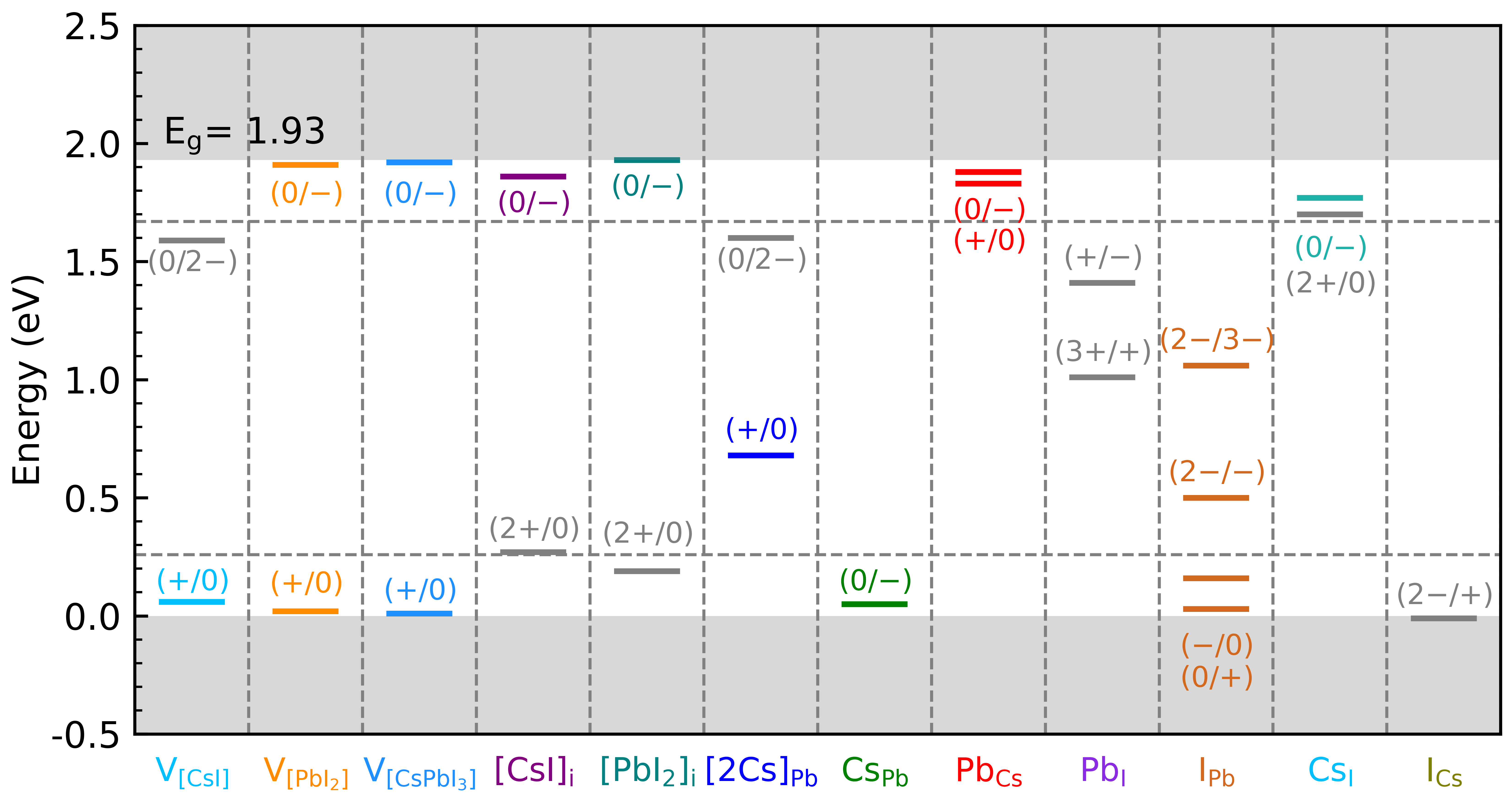
3.4 Charge State Transition Levels
Based on Figure 2 and Eq. (11), the CSTLs of compound defects are determined. The results for all defects considered in this paper, are shown in Figure 4. The most prominent compound defect, the cation-cation antisite , leads to double shallow donor levels, whereas the antisite only leads to a shallow acceptor level. The compound vacancies and have both a shallow donor, as well as a shallow acceptor level. The anion-cation antisite has no levels inside the band gap.
At the intrinsic Fermi level, or indeed if the Fermi level is well inside the band gap, these are all compound defects that can occur in appreciable quantities, see Figure 3(b). If the Fermi level is close to the CBM, the concentration of antisites increases. Although this antisite introduces two deep levels inside the band gap, both of these levels involve a change in charge state of two electrons, i.e., and . These levels are likely to be much less active than donor or acceptor levels associated with a change of one in charge state, as the probability of trapping two electrons simultaneously is very low 36, 19. If the Fermi level becomes extremely close to the VBM, the concentration of becomes non-negligible. As its CSTL (+/0) is well inside the band gap, this compound defect forms a deep trap, which can act as a harmful recombination center.
Besides the defects discussed in the previous two paragraphs, all other defects occur in such negligible quantities, that their electronic impact is negligible. In fact, the only compound defect considered in this paper that forms a series of deep trap levels, which is the anion-cation antisite , Figure 3(b), has a very large positive reaction energy, Table 1, so it does not form under practical conditions.
In summary, the relatively abundant compound defects either form shallow donor or acceptor levels (, , , , ,) or electronically not very active levels (). Only under relatively extreme conditions, with a Fermi level very close to the VBM, the compound defect can form, which has a deep trap level.
4 Conclusions
To conclude, we have studied the formation of compound defects in the archetype inorganic halide perovskite CsPbI3 by means of DFT calculations using the accurate and efficient SCAN+rVV10 functional. Considering compound vacancies, , , and , compound interstitials and , cation-cation antisites, , , , and anion-cation antisites , , , , we evaluate their formation under equilibrium conditions, and under conditions that reflect their formation as recombination reactions of simple point defects.
Although the energies of several of these recombination reactions are favorable, under equilibrium conditions at room temperature, only the formation of the antisite where Pb substitutes Cs is prominent, and the concentrations of point defects are too small to give any appreciable amount of other compound defects. However, under nonequilibrium conditions, mimicked by a high temperature annealing step, several types of compound defects can be formed in significant concentrations. Most prominent are the cation-cation antisites and , with concentrations comparable to those of the dominant point defects and . Smaller amounts of the compound vacancies and , and the anion-cation antisite can be observed, whereas the concentrations of other defects are negligible.
Under solar cell operating conditions the (quasi) Fermi level can shift to the proximity of the VBM and CBM, which promotes the formation of certain compound defects, and suppresses that of others. If the Fermi level is close to the CBM, the formation of and is suppressed, and that of the cation-anion antisite is promoted, whereas if the Fermi level is close to the VBM, the formation of is suppressed, and that of is promoted. The other defects are less affected by a change in Fermi level.
The antisites and compound vacancies that can occur in appreciable concentrations (, , , and ) create shallow trap levels only. The antisite creates several deep levels, which are, however, not very active electronically, as their charge state transition involves the arrival of two electrons simultaneously. Only the compound defect leads to a deep trap level. However, as discussed above, this defect is only likely to form if the Fermi level is very close to the VBM. These results illustrate the exemplary electronic tolerance of halide perovskites towards the presence of defects.
H.X. acknowledges funding from the China Scholarship Council (CSC, No. 201806420038). S.T. acknowledges funding from the Computational Sciences for Energy Research (CSER) tenure track program of Shell and NWO (Project No. 15CST04-2) and the NWO START-UP grant from the Netherlands.
A list of number of possible defect sites and counting rule for each compound defect; Concentration of compound defects at 300 K; Temperature dependence of concentrations of point defects; Table of concentrations of point defects at 300 K and 500 K; Detailed comparison of reaction energies and formation energies of each compound defect.
References
- National Renewable Energy Laboratory 2022 National Renewable Energy Laboratory, Best Research-Cell Efficiency Chart. 2022; https://www.nrel.gov/pv/cell-efficiency.html
- Kim et al. 2016 Kim, H. S.; Seo, J. Y.; Park, N. G. Material and Device Stability in Perovskite Solar Cells. ChemSusChem 2016, 9, 2528–2540
- Zhou and Zhao 2019 Zhou, Y.; Zhao, Y. Chemical stability and instability of inorganic halide perovskites. Energy Environ. Sci. 2019, 12, 1495–1511
- Park and Seok 2019 Park, B.-w.; Seok, S. I. Intrinsic Instability of Inorganic–Organic Hybrid Halide Perovskite Materials. Adv. Mater. 2019, 31, 1805337
- He et al. 2020 He, S.; Qiu, L.; Ono, L. K.; Qi, Y. How far are we from attaining 10-year lifetime for metal halide perovskite solar cells? Mater. Sci. Eng. R Reports 2020, 140, 100545
- Yuan and Huang 2016 Yuan, Y.; Huang, J. Ion Migration in Organometal Trihalide Perovskite and Its Impact on Photovoltaic Efficiency and Stability. Acc. Chem. Res. 2016, 49, 286–293
- Yang et al. 2016 Yang, J.-H.; Yin, W.-J.; Park, J.-S.; Wei, S.-H. Fast self-diffusion of ions in CH 3 NH 3 PbI 3 : the interstiticaly mechanism versus vacancy-assisted mechanism. J. Mater. Chem. A 2016, 4, 13105–13112
- Eames et al. 2015 Eames, C.; Frost, J. M.; Barnes, P. R. F.; O’Regan, B. C.; Walsh, A.; Islam, M. S. Ionic transport in hybrid lead iodide perovskite solar cells. Nat. Commun. 2015, 6, 7497
- Azpiroz et al. 2015 Azpiroz, J. M.; Mosconi, E.; Bisquert, J.; De Angelis, F. Defect migration in methylammonium lead iodide and its role in perovskite solar cell operation. Energy Environ. Sci. 2015, 8, 2118–2127
- Pols et al. 2021 Pols, M.; Vicent-Luna, J. M.; Filot, I.; van Duin, A. C. T.; Tao, S. Atomistic Insights Into the Degradation of Inorganic Halide Perovskite CsPbI3: A Reactive Force Field Molecular Dynamics Study. J. Phys. Chem. Lett. 2021, 12, 5519–5525
- Mosconi et al. 2015 Mosconi, E.; Azpiroz, J. M.; Angelis, F. D. Ab Initio Molecular Dynamics Simulations of Methylammonium Lead Iodide Perovskite Degradation by Water. Chem. Mater. 2015, 27, 4885–4892
- Aristidou et al. 2017 Aristidou, N.; Eames, C.; Sanchez-Molina, I.; Bu, X.; Kosco, J.; Islam, M. S.; Haque, S. A. Fast oxygen diffusion and iodide defects mediate oxygen-induced degradation of perovskite solar cells. Nat. Commun. 2017, 8, 15218
- Tan et al. 2020 Tan, S.; Yavuz, I.; Weber, M. H.; Huang, T.; Chen, C. H.; Wang, R.; Wang, H. C.; Ko, J. H.; Nuryyeva, S.; Xue, J. et al. Shallow Iodine Defects Accelerate the Degradation of -Phase Formamidinium Perovskite. Joule 2020, 4, 2426–2442
- Barker et al. 2017 Barker, A. J.; Sadhanala, A.; Deschler, F.; Gandini, M.; Senanayak, S. P.; Pearce, P. M.; Mosconi, E.; Pearson, A. J.; Wu, Y.; Srimath Kandada, A. R. et al. Defect-Assisted Photoinduced Halide Segregation in Mixed-Halide Perovskite Thin Films. ACS Energy Lett. 2017, 2, 1416–1424
- de Walle and Neugebauer 2004 de Walle, C. G. V.; Neugebauer, J. First-principles calculations for defects and impurities: Applications to III-nitrides. J. Appl. Phys. 2004, 95, 3851–3879
- Freysoldt et al. 2014 Freysoldt, C.; Grabowski, B.; Hickel, T.; Neugebauer, J.; Kresse, G.; Janotti, A.; Van de Walle, C. G. First-principles calculations for point defects in solids. Rev. Mod. Phys. 2014, 86, 253–305
- Yin et al. 2014 Yin, W.-J.; Shi, T.; Yan, Y. Unusual defect physics in CH3NH3PbI3 perovskite solar cell absorber. Appl. Phys. Lett. 2014, 104, 63903
- Shi et al. 2015 Shi, T.; Yin, W.-J.; Hong, F.; Zhu, K.; Yan, Y. Unipolar self-doping behavior in perovskite CH3NH3PbBr3. Appl. Phys. Lett. 2015, 106, 103902
- Meggiolaro and De Angelis 2018 Meggiolaro, D.; De Angelis, F. First-Principles Modeling of Defects in Lead Halide Perovskites: Best Practices and Open Issues. ACS Energy Lett. 2018, 3, 2206–2222
- Huang et al. 2018 Huang, Y.; Yin, W.-J.; He, Y. Intrinsic Point Defects in Inorganic Cesium Lead Iodide Perovskite CsPbI3. J. Phys. Chem. C 2018, 122, 1345–1350
- Meggiolaro et al. 2019 Meggiolaro, D.; Mosconi, E.; De Angelis, F. Formation of Surface Defects Dominates Ion Migration in Lead-Halide Perovskites. ACS Energy Lett. 2019, 4, 779–785
- Xue et al. 2022 Xue, H.; Brocks, G.; Tao, S. Intrinsic defects in primary halide perovskites: A first-principles study of the thermodynamic trends. Phys. Rev. Mater. 2022, 6, 055402
- Xue et al. 2021 Xue, H.; Brocks, G.; Tao, S. First-principles calculations of defects in metal halide perovskites: A performance comparison of density functionals. Phys. Rev. Mater. 2021, 5, 125408
- Kye et al. 2018 Kye, Y. H.; Yu, C. J.; Jong, U. G.; Chen, Y.; Walsh, A. Critical Role of Water in Defect Aggregation and Chemical Degradation of Perovskite Solar Cells. J. Phys. Chem. Lett. 2018, 9, 2196–2201
- Kim et al. 2014 Kim, J.; Lee, S.-H.; Lee, J. H.; Hong, K.-H. The Role of Intrinsic Defects in Methylammonium Lead Iodide Perovskite. J. Phys. Chem. Lett. 2014, 5, 1312–1317
- Keeble et al. 2021 Keeble, D. J.; Wiktor, J.; Pathak, S. K.; Phillips, L. J.; Dickmann, M.; Durose, K.; Snaith, H. J.; Egger, W. Identification of lead vacancy defects in lead halide perovskites. Nat. Commun. 2021 121 2021, 12, 1–7
- Agiorgousis et al. 2014 Agiorgousis, M. L.; Sun, Y.-Y.; Zeng, H.; Zhang, S. Strong Covalency-Induced Recombination Centers in Perovskite Solar Cell Material CH3NH3PbI3. J. Am. Chem. Soc. 2014, 136, 14570–14575
- Pols et al. 2022 Pols, M.; Hilpert, T.; Filot, I.; van Duin, A. C. T.; Calero, S.; Tao, S. What Happens at Surfaces and Grain Boundaries of Halide Perovskites: Insights from Reactive Molecular Dynamics Simulations of CsPbI3. 2022; https://arxiv.org/abs/2205.10545v1
- Kresse and Hafner 1993 Kresse, G.; Hafner, J. Ab initio molecular dynamics for liquid metals. Phys. Rev. B 1993, 47, 558–561
- Kresse and Furthmüller 1996 Kresse, G.; Furthmüller, J. Efficient iterative schemes for ab initio total-energy calculations using a plane-wave basis set. Phys. Rev. B 1996, 54, 11169–11186
- Kresse and Furthmüller 1996 Kresse, G.; Furthmüller, J. Efficiency of ab-initio total energy calculations for metals and semiconductors using a plane-wave basis set. Comput. Mater. Sci. 1996, 6, 15–50
- Peng et al. 2016 Peng, H.; Yang, Z.-H.; Perdew, J. P.; Sun, J. Versatile van der Waals Density Functional Based on a Meta-Generalized Gradient Approximation. Phys. Rev. X 2016, 6, 41005
- Komsa et al. 2012 Komsa, H. P.; Rantala, T. T.; Pasquarello, A. Finite-size supercell correction schemes for charged defect calculations. Phys. Rev. B 2012, 86, 045112
- Wiktor et al. 2017 Wiktor, J.; Rothlisberger, U.; Pasquarello, A. Predictive Determination of Band Gaps of Inorganic Halide Perovskites. J. Phys. Chem. Lett. 2017, 8, 5507–5512
- Tao et al. 2019 Tao, S.; Schmidt, I.; Brocks, G.; Jiang, J.; Tranca, I.; Meerholz, K.; Olthof, S. Absolute energy level positions in tin- and lead-based halide perovskites. Nat. Commun. 2019, 10, 2560
- Tress 2017 Tress, W. Perovskite Solar Cells on the Way to Their Radiative Efficiency Limit – Insights Into a Success Story of High Open-Circuit Voltage and Low Recombination. Advanced Energy Materials 2017, 7, 1602358