SAGE: Software-based Attestation for GPU Execution
Abstract
With the application of machine learning to security-critical and sensitive domains, there is a growing need for integrity and privacy in computation using accelerators, such as GPUs. Unfortunately, the support for trusted execution on GPUs is currently very limited – trusted execution on accelerators is particularly challenging since the attestation mechanism should not reduce performance.
Although hardware support for trusted execution on GPUs is emerging, we study purely software-based approaches for trusted GPU execution. A software-only approach offers distinct advantages: (1) complement hardware-based approaches, enhancing security especially when vulnerabilities in the hardware implementation degrade security, (2) operate on GPUs without hardware support for trusted execution, and (3) achieve security without reliance on secrets embedded in the hardware, which can be extracted as history has shown.
In this work, we present SAGE, a software-based attestation mechanism for GPU execution. SAGE enables secure code execution on NVIDIA GPUs of the Ampere architecture (A100), providing properties of code integrity and secrecy, computation integrity, as well as data integrity and secrecy – all in the presence of malicious code running on the GPU and CPU. Our evaluation demonstrates that SAGE is already practical today for executing code in a trustworthy way on GPUs without specific hardware support.
Index Terms:
GPU, Trusted Execution, Attestation, CUDA1 Introduction
Fueled by recent trends such as machine learning and the declining yields from Moore’s Law, the use of accelerators to process the vast volumes of data is becoming indispensable. In fact, it is expected that the majority of compute cycles in public clouds will be executed on accelerators [1].
With the application of machine learning to security-critical or sensitive domains such as healthcare or financial modeling, there is a growing need for a mechanism that maintains integrity and secrecy for both code and data despite the computation being offloaded to the GPU.
With the wide-spread deployment of trusted execution environments (TEEs), e.g., Intel SGX [2] and ARM TrustZone [3], an important question is how security-sensitive computation tasks can be accomplished on GPUs. While first hardware-based TEEs on GPUs are starting to emerge [4, 5, 6, 7, 8, 9], how can we execute code securely on GPUs in current environments? As we have witnessed from the introduction of hardware-based TEEs on x86 platforms, it took over a decade until it became possible to fully and widely utilize these mechanisms. At the same time, technology progress in this space is a moving target as new attacks (among other factors) force vendors to phase out one specific hardware-based technology in favor of more robust successors (such as with the case of the deprecation of Intel SGX [10]). Given the importance of software executing on GPUs, it is clear that we need to find approaches to speed up the long lag time between deployment and wide-spread utilization.
A promising approach for bridging this gap is a software-only approach to trusted execution. In the context of CPU-based execution, a rich research field has contributed numerous approaches [11, 12, 13, 14]. The basic approach of the prior software-based or timing-based attestation approaches was to design a verification function that would run on an untrusted system and compute a checksum over itself – where both the correctness of the checksum and the time duration are measured by a trusted verifier. A correct checksum value that is returned before a threshold point in time, indicated to the verifier that the TEE was correctly set up and that the correct code is now executing (code integrity and launch point integrity). In combination with a system for control-flow verification, control-flow integrity can also be achieved.
The challenge of such software-based TEE establishment approaches lies in the creation of a verification function that will slow down noticeably or produce an incorrect checksum, if an adversary attempts to tamper with its execution.
The creation of a verification function for GPU environments poses numerous research challenges, which may be the reason why it has so far not been achieved, to the best of our knowledge. First and foremost, achieving (1) code secrecy and integrity, and (2) data secrecy and integrity, (3) in the presence of a malicious OS, (4) malicious code on GPU, and (5) a malicious CPU-GPU interconnect is a formidable challenge. Other challenges that we had to overcome include the absence of a true random number generator on the GPU, the lack of documentation from GPU vendors for a specific target architecture, no toolchain support to write native GPU code, and achieving an optimal GPU utilization.
We design the SAGE system, which establishes a TEE on NVIDIA GPUs of the Ampere architecture (A100). SAGE utilizes an SGX enclave running on the host to act as a local verifier, and to bootstrap the software primitive to establish a dynamic root-of-trust (RoT) on the GPU. RoT establishment ensures either that the state of an untrusted system contains all and only content chosen by a trusted local verifier and the system code begins execution in that state, or that the verifier discovers the existence of unaccounted content. SAGE also sets up a shared secret key between the verifier and the GPU, which can be used to establish a secure channel to achieve integrity and secrecy for code and data transferred. Our results indicate that after a successful invocation of SAGE, the verifier obtains assurance that: (1) the user kernel on the untrusted device is unmodified; (2) the user kernel is invoked for execution on the untrusted device; and (3) the executable is executed untampered, despite the potential presence of a malicious actor.
This paper presents the following contributions:
-
•
We design a software-based attestation mechanism for GPU execution that enables secure code execution on NVIDIA Ampere GPUs, providing code integrity and secrecy, computation integrity, as well as data integrity and secrecy.
-
•
We implement an instruction generation framework that is capable to generate GPU microcode. This requires understanding the GPU architecture and the instruction format used in microcode, which we obtained using a instruction decoding framework.
-
•
We implement a true random number generator (TRNG) for execution on GPU based on race-conditions.
-
•
Through a proof-of-concept implementation on the NVIDIA A100 platform, we demonstrate the technical feasibility of the approach.
2 Background: GPU Fundamentals
In the following, we describe the fundamentals of NVIDIA GPUs and their programming model (CUDA) to illustrate how compute tasks are offloaded and executed on the GPU. We focus on mechanisms relevant to this work.
The GPU is connected via the PCI control engine to the host CPU and uses an internal bus for communication between its core components. The core components are the command processor, compute and DMA engines, and the memory system, consisting of a memory controller, registers, on-chip and device memory.
Controlling the GPU
Commands to the GPU are transmitted using a set of command queues known as channels. The GPU’s command processor receives these commands and forwards them to the corresponding engines.
Data transfer to the GPU
GPU programming inevitably incurs data transfers between host and device memory. This is handled using direct memory access (DMA). The copy engine is responsible for handling DMA commands and their corresponding memory accesses.
GPU execution
The GPU’s compute engine contains multiple Processor Clusters (PCs), each containing multiple Streaming Multiprocessors (SMs). SMs are partitioned into multiple processing blocks, each containing specialized processing cores (e.g., INT32 cores), a scheduler and a dispatch unit. GPU kernels to be executed on the GPU are scheduled to SMs and specify the number of threads to be created. These threads are organised in thread blocks and grids. Thread blocks are divided into warps. Each warp is a group of parallel threads and gets scheduled by a warp scheduler.
Execution is context-based, where a context represents a collection of resources and state that is required to execute a GPU kernel. Resources on the GPU are allocated per context and freed upon its destruction. Each context has its own assigned address space and allocates at least one channel to receive commands. However, on current GPUs there is no isolation between contexts that prevents them from accessing each other’s resources.
Modern GPUs have multiple processing pipelines [15] for different data types. The FMA pipeline executes 32-bit floating point instructions and integer multiply and add (IMAD). The ALU pipeline executes 32-bit integer, logical, binary, and data movement operations. In addition, there are also pipelines for 64-bit and 16-bit floating point, and Tensor core operations. The FMA and ALU pipeline have a separate dispatch port with a warp dispatch latency of two cycles. Concurrent execution is achieved by alternating instruction dispatch to different pipelines. The other pipelines use the same dispatch port and concurrent dispatching to these pipelines is not possible.
GPU memory system
The memory system on GPUs consists of a memory controller and different memory levels. The memory levels are associated to the compute system as follows (see Figure 1). Each processing block includes an L0 instruction cache and a register file. The combined processing blocks of a SM share a combined L1 data cache/shared memory that can be partitioned depending on the workload. Multiple SMs share an L2 cache before pulling data from global (off-chip) GDDR memory. Registers are a shared resource and are allocated among the thread blocks executing on a SM with a granularity of . Accessing a register consumes zero extra clock cycles per instruction, but delays may occur due to register read-after-write dependencies and register memory bank conflicts. In case a thread requires more registers than available, the data contained in the registers is spilled into shared memory. Shared memory is not only used for register spilling, but also enables cooperation between threads in a block. When multiple threads in a block use the same data from global memory, shared memory can be used to access the data from global memory only once.
3 Problem Definition
In this section, we describe the design goals we strive to achieve, as well as the assumptions and the adversary model we consider.
3.1 Design Goals
Verifiable code execution on the GPU
Verifiable code execution describes the problem in which a verifier wants a guarantee that some arbitrary code has executed untampered on an untrusted platform, despite the potential presence of a malicious entity (e.g., malicious software) [12]. This problem is typically approached by verifying code integrity through root of trust attestation, setting up an untampered code execution environment, and then executing the code.
Data integrity and confidentiality
In addition to code integrity also the integrity and/or confidentiality of the data executed on the GPU must be ensured. Specifically, we wish to guarantee that the adversary cannot observe or tamper data transferred to/from the GPU by a trusted application that runs in a CPU TEE.
Dynamic root of trust without hardware support
Dynamic root of trust establishment denotes the problem of dynamically setting up a trusted computing base (TCB) on an untrusted platform without hardware support. All code contained in the dynamic root of trust is guaranteed to be unmodified and it can thus be used to provide externally verifiable code execution.
Practical to run on a GPU architecture.
The attestation mechanism must be practical to run in a high performance environment with thousands of cores and high memory bandwidth [16] while not impacting the performance of the verified program.
3.2 Assumptions
Verifier and GPU on the same machine
We assume that the verifier is executed on the same machine as the GPU we want to attest. The GPU is directly connected to the host CPU over a bus (e.g., PCIe with a latency of ~ [17]).
GPU hardware configuration
We assume that the verifier knows the exact hardware configuration of the GPU, including the GPU model, the number of cores, the memory architecture, and the GPU clock speed.
Multi-GPU environments
In heterogeneous multi-GPU environments, we assume that our verification function runs on the fastest GPU available. In homogeneous multi-GPU systems, an arbitrary GPU can be selected for computation. Consequently, the adversary cannot get a performance advantage by running code on other available GPUs. Furthermore, the dynamic RoT could also be established in sequence (while actively maintaining already established RoTs) starting from the most powerful GPU to the least powerful GPU.
3.3 Threat Model
In the following, we discuss the threat model consider by defining the trusted compute base (TCB) and outlining the capabilities of an adversary. The TCB of a system refers to all hardware and software components that are critical to its security, in the sense that bugs or vulnerabilities occurring inside the TCB might jeopardize the security properties of the entire system.
Trusted compute base (TCB)
We assume an adversary who has complete control over the untrusted host system. In other words, the adversary has administrative privileges, can tamper with the entire system software, the operating system, or the guest operating system and the hypervisor in case of virtualization. However, we assume that the hardware primitives of the CPU and GPU, and CPU’s firmware are contained in the TCB. Since SAGE uses Intel SGX, it inherits the TCB of SGX (which includes the CPU package, trusted libraries, etc.). In addition, SAGE’s TCB comprises of the user-space GPU runtime and the GPU driver. The runtime is used to program the GPU and transfer data between host and device memory, whereas the GPU driver is responsible for submitting commands to the GPU via the PCI bus and for managing the device. Currently neither the GPU driver nor the GPU runtime are part of SGX. Integrating them into SGX is considered out-of-scope for SAGE, but could be addressed in future work by porting an open-source driver such as nouveau [18] to SGX. Furthermore, a GPU vendor could also decide to port their proprietary drivers and runtime to SGX.
In addition, we assume that the adversary has physical access to all system hardware, including the GPU. But the adversary cannot perform any physical attacks on the GPU’s chip.
Capabilities
Considering these capabilities, an adversary can read and tamper with code or data of any victim process, and can access or modify data in DMA buffers or commands submitted to the GPU. Furthermore, the adversary could inject packets in arbitrary locations on the I/O communication path between the host and the GPU. This gives the adversary control over attributes, such as the address of GPU kernels being executed and parameters passed to the kernels. The adversary may also access device memory directly over MMIO, or map a user’s GPU context memory space to a channel controlled by the adversary. Given the physical access to the system, the adversary can mount eavesdropping attacks on the host memory and PCIe bus. In GPUs that support multi-tasking, malicious kernels can be dispatched to the GPU, thereby accessing memory belonging to a victim’s GPU context. Since the adversary controls the hypervisor and thus the mapping between VMs and virtual devices, these attacks are possible even in a virtualized environment.
Out of scope
Since this work tackles the problem of trusted execution on the GPU, we do not consider attacks that target the defense of SGX, such as physical attacks to the CPU package or side-channel attacks on SGX. In addition, we do not consider system availability attacks that prevent the execution of our process, as an adversary with the described capabilities can always prevent the deployment of computing tasks on the GPU.
4 SAGE Overview
SAGE addresses the problem of verifiable code execution on a GPU without hardware support, in which the verifier wants a guarantee that some arbitrary code (i.e., the user kernel) has executed untampered on an untrusted GPU platform, even in the presence of an adversary. Figure 2 illustrates the abstract system model we consider.
SAGE comprises of two main components. The first component is the verifier, which runs as a trusted application on the host CPU (e.g., using Intel SGX [2]) and is attested by an external challenger. The second component is the verification function (VF), which runs on the the untrusted GPU. The VF computes a checksum over its own code, and is constructed in an intricate way such that if a change is applied to the VF then either the execution will slow down in an externally detectable manner, or the checksum value will be incorrect.
The verifier dispatches to the GPU the VF and then invokes it repeatedly with a series of challenges while measuring the VF execution time for each invocation. For every challenge, the VF computes a checksum value and returns it to the verifier. Using the same VF logic, the verifier independently computes and verifies the correctness of the checksum value. If the checksum returned by the VF is correct and it is returned within the expected time, the verifier obtains a guarantee that a dynamic root of trust on the GPU was established.
Once the dynamic root of trust has been established, the VF checks the integrity of the user kernel, sets up an untampered execution environment, and finally runs the user kernel. During the setup of the execution environment, a shared key between the verifier enclave and GPU is established; afterwards, only commands authenticated with this key are accepted, including the movement of (encrypted if needed) data between host and GPU. Figure 3 shows an overview of SAGE including a sequence of events.
5 Verification Function (VF)
The VF that runs on the untrusted GPU is the fundamental component of SAGE. We now describe in detail these tasks and the challenges that they entail.
5.1 Design Requirements
The VF must be carefully constructed in such a way that if an adversary were to tamper with the VF or the user kernel, it would result in either a wrong checksum or a noticeable time delay. Before offering a concrete design for the VF, we describe several required properties and outline how these properties influence the correctness of the checksum or the VF execution time. We defer our security analysis to § 8; the following properties also account for the attack surface analyzed therein.
-
1.
Time-optimal implementation. The implementation of the VF must be time-optimal. Otherwise, the adversary could use a faster implementation and use the time saved to forge the checksum (e.g., by injecting instructions).
-
2.
Maximize resource usage during checksum computation. To prevent the adversary from running any other computation during the checksum computation, the VF should maximize its resource usage on the GPU by using all available SMs and avoiding “empty” threads. Moreover, each thread should use the maximum number of available registers to prevent the adversary from using those registers. Thus, if the (tampered) computation attempts to use more registers than available, the values of the affected registers are spilled into shared memory, resulting in a noticeable execution time difference (4- vs. 30-cycle latency for registers and shared memory, resp.).
-
3.
Predictable execution time. The execution on GPUs is optimized to achieve high data throughput with determinate latency, but the execution time is non-deterministic (e.g., due to multi-threaded execution, scheduling, and caching). The VF execution time should have low variance so that the verifier can predictably determine the correct execution time.
-
4.
Challenge-dependent checksums. To prevent the adversary from pre-computing the checksum before making changes to the VF, and to prevent the replay of old checksum values, the checksum needs to depend on an unpredictable challenge sent by the verifier.
-
5.
Strongly-ordered checksum code. A strongly-ordered function is a function whose output differs with high probability if the operations are evaluated in a different order. If the adversary attempts to gain an advantage by altering the order in which single instructions or entire sequences of instructions are executed, the verifier should receive a wrong checksum or record a noticeable increased execution time.
-
6.
Include architectural complexity. Subtle data attacks need to be prevented (more details in § 8). For instance, the adversary can keep a correct copy of any memory location in the tampered VF and when the checksum computation attempts to read one of the modified memory locations, the read is redirected to the location where the adversary has stored the correct copy. To maximize the time overhead for such attacks, the checksum computation should include some architectural complexity (e.g., a pseudo-random memory access).
5.2 Concrete VF Design
The VF consists of four parts: 1) initialization, 2) self-verifying checksum function to establish a dynamic root-of-trust, 3) establishing an untampered execution environment (including a key establishment protocol between the verifier and the GPU), and 4) a hash function to measure the integrity of the user kernel. We describe each in the following.
5.2.1 Initialization of the VF
During the initialization phase, the verifier dispatches the VF code to the GPU. For this purpose the GPU first allocates a memory buffer and returns the buffer’s base address to the verifier. The code of the VF is then copied into the buffer at specific offsets.
5.2.2 Self-Verifying Checksum Function
The checksum function is used to obtain a guarantee that the integrity of the VF code running on the GPU is unaffected by an adversary. For this purpose, the checksum function computes a checksum over the entire VF code. The resulting checksum can be used as a fingerprint of the VF and enables detection of changes to the VF code. If an adversary modifies the VF code, the checksum will differ with high probability. Thus, once the verifier receives a correct checksum within a threshold time, it has a guarantee that the VF code running on the GPU is unmodified.
Since the checksum computation code is part of the VF and will thus be included in the checksum calculation, the checksum function computes the checksum over its own instruction sequence and verifies itself. This property is further referred to as self-verification.
Checksum initialization
GPUs contain multiple multiprocessors that can be used for parallel execution. To exhibit the maximal computational power of a GPU, the verifier sends a set of challenges containing a specific challenge value for each multiprocessor. Upon receiving a set of challenges, each multiprocessor uses its challenge as a seed value to initialize all per-thread state with random data and a pseudo-random number generator (PRNG) that is used during the checksum computation. Each thread has its own set of registers which are used to store the running checksum values and a data pointer. The data pointer references the VF code in the initially allocated buffer (§ 5.2.1).
Self-modifying code
In memory copy attacks, the adversary replaces the checksum function with an altered version and executes it (described in detail in § 8). To prevent memory copy attacks, the execution state – namely, the program counter (PC) and data pointer (DP) – needs to be included in the computation of the checksum.
The GPU maintains execution state per thread, including a program counter and call stack, however, does not expose it to the high-level programming models. In the low-level programming models, the current PC could be loaded into a register using instruction patching (LEPC instruction, see § 6.2). However, loading the PC into a register and including it into the checksum computation does not prevent memory copy attacks. An adversary could replace the instruction used to load the PC with a move instruction with an constant immediate value without causing any computational overhead. An alternative to directly loading the PC to prevent memory copy attacks could employ boundary checks (e.g., the DP needs to be in close proximity to the PC), but could be circumvented by an attacker in the same way.
Instead of directly including the PC in the checksum computation, we use self-modifying code, such that the execution of these instructions depends on the current value of the checksum. If the adversary wants to successfully execute a memory copy attack, he would need to closely monitor the execution of the checksum function and modify the instruction in its copy accordingly. This manipulation of the code in two location causes a constant time overhead in each execution of the self-modifying code.
Checksum loop
The checksum computation is performed iteratively where each iteration contains the following steps. Each iteration executes the same number and type of instructions and has a constant execution time. However, the self-modifying code depends on the current checksum value and thus changes in each iteration.
-
1.
Pseudo-random memory access of VF code. In data substitution attacks (see § 8 for details) the adversary keeps a correct copy of any memory location in the VF code it modifies and attempts to redirect all memory reads that access the modified memory location with reads of the correct copy it has stored. Thus, the adversary’s checksum result will be correct despite the modification of the VF. To maximize the adversary’s time overhead for this attack, the checksum code reads the memory region containing the VF code in a pseudo-random pattern. This pseudo-random memory access prevents the adversary from predicting which memory-resident instruction will read the potentially-modified memory location and forces the adversary to monitor every memory read by the checksum code.
-
2.
Update the checksum. The running checksum values are updated to include the accessed VF code into the checksum value using a sequence of instructions. To achieve a time-optimal implementation, we use simple arithmetic and logical instructions (e.g., add, <<, >>, etc.) that are challenging to implement faster or with fewer operations. Taking inspiration from the strong ordering used in [12], the instructions used to update the checksum alternate between arithmetic and logical instructions to enforce a strong ordering of the instructions. Including the pseudo-randomly accessed VF code segment enables self-verification of the checksum function.
-
3.
Include the data pointer. In the next step, the data pointer that is kept as a running value in each thread is included into the checksum. This ensures that the memory region is untampered and prevents memory copy attacks that tamper the VF, but keep a copy of the original VF in a different memory location (see § 8).
-
4.
Self-modifying code. The instructions of the self-modifying code depend on current value of the checksum function and are changed in each iteration of the checksum function. In our case the current value of the checksum function is used as an immediate value for an instruction (see § 6.5 for details).
If an adversary alters the checksum function but wants to forge a correct checksum output, he has to manipulate the values of one or more of the inputs in every iteration of the checksum code, causing a constant time overhead per iteration.
Checksum epilog
Since the checksum computation is conducted using individual threads located on different multiprocessors, the checksum values need to be aggregated before sending the checksum result back to the verifier. This aggregation is conducted in three steps. First, we aggregate the checksum per warp. Each of the per-thread checksums is added pairwise to obtain a warp-level checksum. Second, the warp-level checksums are aggregated by thread block using shared memory. Finally, we aggregate the checksum per grid using global memory. Each of the aggregation steps uses a pairwise addition (which is mapped to an atomic add instruction in native assembly). The final result of the checksum computation is then sent to the verifier.
5.2.3 Untampered Execution Environment
After establishing a dynamic root-of-trust on the device, the VF sets up an execution environment in which the user kernel is guaranteed to run untampered. This includes setting up a shared secret between the verifier and the device, and checking the authenticity of the user kernel to be executed on the GPU using a hash function. The shared secret can then be used to authenticate and encrypt commands and data sent by the verifier to the device and vice versa.
Key establishment
To establish a shared secret between the verifier and the device, we rely on the SAKE protocol [19], a protocol for key establishment between neighboring nodes in sensor networks without requiring any prior secrets. The protocol is based on the Diffie-Hellman key exchange protocol and uses the Guy Fawkes protocol [20] for authentication. The Guy Fawkes protocol is based on hash chains and relies on the property that each of the participants needs to authenticate the other party’s hash chain. In SAKE, this authentication is achieved using software-based attestation and exploits the asymmetry in the checksum value and the computing time between the genuine checksum function and a modified checksum function. This allows us to use the resulting checksum as a short-lived “secret.” Furthermore, the SAKE protocol assumes that the adversary does not introduce any computationally powerful nodes into the network, which aligns with the assumptions for SAGE (see § 3.2).
To apply the SAKE protocol to SAGE, we change the protocol as follows: 1) The checksum function in SAKE that was proposed for the use in sensor networks is replaced with SAGE’s checksum function. 2) Instead of both participants acting as challengers, only the host enclave will engage as a challenger. 3) We replace the cryptographic primitives used in the protocol with AES-CMAC as the MAC function and SHA256 as the hash function.
Assuming the changes above, the key establishment protocol in SAGE works as follows. First, the verifier sets up its own hash chain and DH public key as:
| (1) |
where is a random bitstring Then, it sends to the device and records the current time as .
| (2) |
Upon receiving , the device uses it as a challenge for the checksum function and then uses the computed checksum and a random value to generate its own hash chain and replies to the verifier:
| (3) |
where is a random bitstring , is the result of the checksum computation and refers to concatenation.
| (4) |
The verifier checks if the measured execution time () matches the expected execution time and aborts the protocol otherwise. In the meantime, the device sets up its own DH public key:
| (5) |
Then, the verifier and the device gradually disclose the remaining of their hash chains to each other:
| (6) | ||||
| (7) |
For each message the recipient checks whether the received value matches the expected hash chain. Finally, the verifier and the device compute the shared secret key :
| (8) |
Authenticity check of user kernel
To check the authenticity of the user kernel, the VF uses a hash function (SHA256) and computes a hash over the user kernel located in memory on the device concatenated with a random value provided by the verifier.
| (9) |
Then, it returns the hash value to the verifier that checks whether it matches the expected hash value.
5.2.4 Protected Data Transfer to the GPU
After the dynamic RoT has been established on the GPU and the integrity of the user kernel has been checked, the host enclave can start transferring data that will be processed by the user kernel to the GPU. Depending on the sensitivity and security criticality of the domains, the data could be either authenticated and/or encrypted using the established symmetric key . For authenticity, the data transfer can already be started while the host enclave is checking the result of the checksum computation. However, if the data must remain confidential, the data transfer must be deferred until the checksum returned by the untrusted device is considered valid.
6 Implementation
To establish the dynamic RoT on the untrusted GPU, SAGE relies on the checksum result, but also measures the execution time of the VF to assess its integrity. This requires a time-optimal implementation of the VF. Otherwise, the adversary could use a faster implementation and use the time saved to forge the checksum (e.g., by injecting instructions). The requirements to achieve a time-optimal implementation on the Ampere architecture (further discussed in § 6.3) include maximizing GPU utilization, consume all available compute resources, optimally filling the processing pipelines, and optimize cache usage.
Unlike the higher levels of the CUDA computing platform such as the CUDA C/C++ language extension and the parallel thread execution (PTX) virtual machine and instruction set architecture, NVIDIA provides very little information about the hardware specific instruction sets for a specific target architecture. Moreover, even if one resorts to write inline PTX virtual assembly, the Streaming (or Shader) Assembler (SASS) code emitted by the compiler often does not achieve the performance of native GPU applications. The execution of microcode that has been compiled using the regular CUDA compiler often is in the order of 10x slower compared to optimized microcode [21, 22]. As a consequence, libraries used for high-performance computing (e.g., cuBLAS [23]) contain highly optimized microcode tailored to a specific architecture. In addition to the performance gap to native GPU code, the user has no control over the translation from PTX virtual assembly to the SASS assembly for the target architecture.
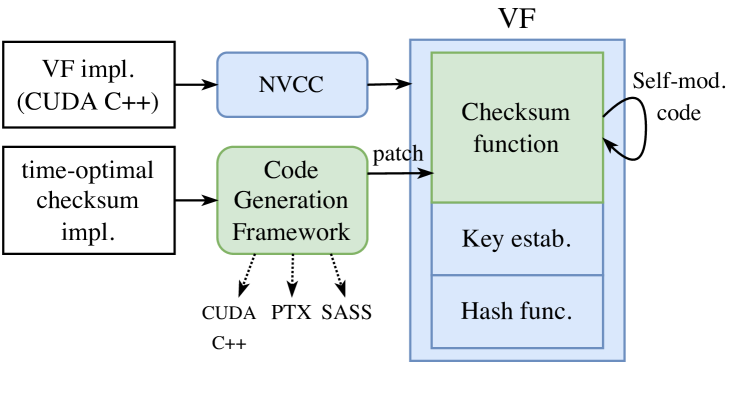
To achieve a time-optimal implementation, we are required to implement a custom instruction generation framework that allows patching of binary microcode with a highly optimized version. The implementation of this framework requires understanding the Ampere architecture and the instruction format used in microcode. Figure 5 illustrates the pipeline used to generate the VF. The VF is implemented using CUDA C++ and compiled using NVCC. However, the section containing the checksum function is patched using an optimized implementation generated as binary microcode using our framework. Our framework and implementation of SAGE can be found here https://github.com/spcl/sage.
6.1 Instruction Decoding
To understand the instruction format used in the recent Ampere GPU architectures, we implemented a framework that allows decoding of instructions using cuobjdump and nvdisasm [24] by decoding handcrafted code samples and samples from existing CUDA libraries (e.g., cuBLAS [23]).
Instruction format
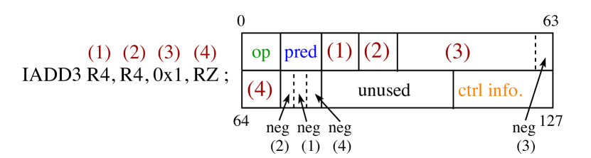
NVIDIA’s Ampere architecture adopts the same general instruction format as its predecessors Turing and Volta [22, 21]. All these architectures use 128 bits to encode both an instruction and its associated scheduling control information. The encoding that is used in these architectures is fixed length and uses similar encodings for all instructions. Figure 6 illustrates a typical instruction encoding.
Control information
The control information section in the instruction encodes scheduling decisions taken by the compiler that the hardware must enforce. The control information is organized as follows: reuse flags (), wait barrier mask (), read barrier index (), write barrier index (), yield flag (), and the number of stall cycles (). The reuse flags allow data reuse between instructions without accessing any register ports. The wait barrier mask and indices are used for instructions with variable latency (e.g., instructions involving a memory access). These dependency barriers can be used to enforce the completion of variable-latency instructions. The yield flag is used to balance the workload assigned to a processing block. The stall cycles indicate the latency of the instruction before issuing the next instruction. Jia et al. present a detailed description of the control information [21].
6.2 Instruction Generation
Understanding the instruction format allows us to generate the specific instructions we need for our implementation. These instructions then need to be translated to the correct binary format. For this purpose, we implement an instruction generation framework that allows emitting instructions either in CUDA C++, the virtual assembly language PTX, or as binary microcode that is natively executed on the GPU.
The instruction can be defined in the following format, where the section separated using pipes describes the control information for the instruction (barrier mask B, read barrier index R, write barrier index W, yield flag Y, and number of stall cycles S):
B......|R.|W.|Y1|S1| IMAD.U32 R28, R28, 2048, R28;
Our instruction generation framework then translates the instruction to the selected target language (CUDA C++, PTX, microcode). This allows us to rapidly prototype checksum functions and compare performance between implementations in each of the languages.
6.3 Time-optimal Technical Requirements
We formulate the following technical requirements for a time-optimal implementation of the checksum function. These are subject to characteristics of the target architecture; in our case, the NVIDIA Ampere architecture.
Maximize resource consumption
To maximize the resource consumption during the checksum computation, the checksum function must use all available compute resources. The NVIDIA A100 GPU has 108 Streaming Multiprocessors (SMs) each containing FP32 and INT32 units [25] that must be used during each clock cycle.
Optimally fill FMA and ALU pipelines
Since both the FMA and ALU pipelines have an instruction issuing latency of clock cycles, FP32 and INT32 instructions must be interleaved to fully saturate both pipelines. In addition, instructions that use registers with a direct dependency must be executed with a latency of at least clock cycles to avoid pipeline stalls (e.g., read-after-write dependency).
Optimal GPU utilization
To achieve full GPU utilization, the number of threads per thread block needs to be picked according to the target architecture. The A100 achieves full GPU occupancy by assigning 2 blocks of size 1024 to all the 108 available SMs (216 total). Each SM has 65,536 32-bit registers available for threads. To use all registers during the checksum computation while maintaining full utilization of the GPU, registers are assigned per thread [26].
Cache size
The code blocks should not exceed the capacity of L0 and L1 instruction caches.
6.4 Selection of Optimal Overheads
An optimal implementation of a checksum function should perform a useful computation step in each clock cycle. In practice, this requires a highly optimized use of the underlying hardware. In the following, we show a recipe for building such a checksum function for the A100 GPU.
Unutilized clock cycles are mainly caused by instruction cache misses, global memory access latency, pipeline stalls, and jumps to the beginning of loops. In the beginning of each clock cycle, the SM warp scheduler selects a subset of warps (up to 4 on A100) from all active warps (up to 64 on A100) to execute. This selection mechanism can avoid performance losses if at least 4 are ready to execute on each clock cycle.
To analyze the performance of the checksum function, we use a simplified model of the number of clock cycles per instruction. We distinguish the total number of useful clock cycles X and overhead cycles Y, so that the total number of clock cycles spent by the code using a single thread is X+Y. For example, with proper instruction ordering to avoid pipeline stalls, an IMAD instruction has X=1 and Y=0. An instruction reading from global memory has X=1 and approximately Y=250. To prevent attacks on the checksum function, the value Y must not exceed X(64/4 - 1). Then, the GPU scheduler will be able to completely hide the overhead Y so that the actual amount of time spent will be X.
Integer shifts and multiplications with addition directly affect the result of the checksum calculation. However, among the useful instructions in X, some do not affect the checksum. One of them is the instruction for jumping from the end of the loop body to its beginning. The attacker may try to unroll a few iterations of the loop to save the clock cycles required to perform this jump (and potentially misuse them for an attack). To prevent such attacks, we unroll the loops until it is not possible to unroll them further without causing instruction cache misses. The target value Y for unrolling must be so large that one additional instruction cache miss will increase it to Y’ such that the hardware scheduler can no longer hide. A similar attack and defense against it applies to other instructions inside the body of the checksum function.
In practice, we have noticed that achieving this level of control over the order of instructions, and the arrangement of unrolled loops is very difficult without vendor support: the documentation on SASS and hardware details is deliberately kept closed ease backward-compatibility hassles. It is especially difficult to control instruction cache misses because of the use of self-modifying code to protect against memory copy attacks. The only way to invalidate the instruction cache on the A100 is to overflow it with the block of instructions of the cache size, so controlling the value of Y by changing the size of the checksum function is not possible. That leaves only memory accesses and jumps that can change Y. We assume that adding an instruction to invalidate the instruction cache requires minimal (or no) changes to the GPU architecture because a similar instruction already exists for the data cache (discard in PTX ISA or CCTL in SASS).
6.5 Implementation of SAGE
Verifier
We implement the verifier enclave using the Intel SGX SDK [27] and its tcrypto library [28]. The enclave creates a CUDA context on the GPU, loads the VF as a module, and calls the VF kernel. To generate nonces in the enclave that are then transferred to the GPU as challenges, we use AES-CTR with an IV that has been generated using a TRNG during the enclave creation.
VF
The VF is implemented in CUDA C++, except the checksum function component, which is patched by binary microcode using our framework. The checksum function executes a loop containing the following steps:
-
1.
The iteration counter is increased and checked if the maximum number of iterations is reached.
-
2.
A data block of the VF is read from memory and will be included into the checksum computation as . The read from main memory takes ~ cycles to be completed. The GPU compiler sets a read barrier for this instruction and the GPU stalls the compute pipeline until the read has been completed. However, stalling the checksum computation would allow the adversary to execute its own instructions.
-
3.
Instead of stalling, we design a pattern of instructions that is executed while waiting for the memory read to be completed (“busy waiting”). This pattern must fully utilize both the FMA and ALU pipeline to which instructions are dispatched alternatingly. To achieve this utilization we use a shift-and-add pattern that can be implemented using a single instruction on both the FMA and ALU pipeline (IMAD and LEA.HI). As a consequence, the previous access to global memory becomes “invisible” in terms of latency.
-
4.
Once the memory load is completed, the checksum is updated using a thread block-specific computation. The block specific computation consists of alternating left or right shifts with addition. Each instruction uses arbitrarily chosen shift size to make sequences of such shifts unique. Then, the current iteration index and the value of unused registers during the computation are incorporated into the checksum.
-
5.
After updating the checksum function, we compute the self-modifying code that consists of the following binary instruction: x+=x>>N, where the immediate N depends on the current checksum value. We overwrite immediate parameter with the current value of the checksum. Thus, the value of changes for each iteration and ensures that we are executing the code that we are verifying. To avoid race conditions when updating the immediate value of these instructions, these instructions are required to be located in different memory areas for each thread block.
Key establishment
For the key establishment protocol based on the modified SAKE protocol, the GPU needs to be able to generate random values. Given that the adversary knows the entire code executing on the GPU, we cannot use a secret provided by verifier to initialize the pseudo-random number generator used in the protocol, but instead must rely on a true random number generator.
6.6 Random Number Generation on GPUs
There are two main categories of random number generators: pseudo-random number generators (PRNG) and true random number generators (TRNG). PRNGs are deterministic, producing the same set of random numbers for a particular input seed, while TRNGs are non-deterministic and typically use a physical source of randomness, whereby every run will produce truly unpredictable random numbers. In SAGE, we require a TRNG implementation to generate keys and seed values for the PRNG that will be used in the key establishment protocol. For the PRNG, we utilize the CUDA random number generation library (cuRAND) [29].
TRNG implementation on GPUs
Approaches that use physical unclonable functions (PUFs) to initialize PRNGs on the GPU [30, 31, 32] are not practical to be used in SAGE as they either require resetting the GPU or use features that are under control of the adversary (e.g., voltage supplied to the GPU). Consequently, we use a TRNG implementation is based on race conditions in multi-core environments caused by simultaneous memory accesses to shared variables and takes advantage of uncertainties that arise when cores simultaneously access a particular memory location [33]. In our case, each simultaneous memory access unpredictably flips bits stored in shared variables. This unpredictability enables the GPU to generate noise which can be sampled and then used as an entropy source. We evaluated our implementation using statistical tests such as NIST SP 800-22 [34], DIEHARD [35], and ENT [36]. The TRNG implementation passes all standard tests and achieves a throughput of on NVIDIA A100 GPUs and thus takes around to generate an output of . The TRNG provides of entropy per byte (measured using ENT [36]).
7 Evaluation
We evaluate the practicality of our approach by evaluating its performance on the NVIDIA A100 GPU and show overheads introduced by the VF compared to a regular execution of the user kernel. Finally, we evaluate the robustness of the VF to potential attacks and show that any additional instructions will result in a detectable overhead.
Evaluation setup
To evaluate the performance of the checksum function, we use an evaluation setup based on an ASUS RS720-E10-RS12E equipped with a Intel Xeon Gold 6348 CPU [37] which natively supports SGX instructions (further referred to as Intel), and a NVIDIA A100 GPU. We run the SGX enclave in both native and simulation mode. To benchmark the execution time of the verification process, we also run the VF on a dual-socket system with an AMD EPYC 7742 CPU (further referred to as AMD).
Register consumption
For the execution of the checksum function, the loop counter, data pointer, and the checksum result are stored in registers. In addition to those registers, we use 22 additional registers to store intermediate state during the computation of the checksum. In total, the checksum function verifies 524,288 bytes. The beginning of the buffer contains the checksum function itself, whereas the remainder is filled with pseudo-randomly generated values.
| Experiment Nr. | 1 | 2 | 3 | 4 |
| self-modifying code | ✗ | ✗ | ✓ | ✓ |
| instructions | 428 | 429 | 8,342 | 8,342 |
| iterations | 100,000 | 100,000 | 1,000 | 1,000 |
| inner iterations | 0 | 0 | 0 | 5000 |
| inner instructions | 0 | 0 | 0 | 216 |
| verification (AMD) [s] | 21.6 | 21.6 | 9.99 | 497 |
| verification (Intel) [s] | 102 | 102 | 47.0 | 2337 |
| runtime [s] | 0.4941 | 0.4977 | 0.1309 | 12.40 |
| % of GPU peak perf. | 99 | 98 | 75 | 100 |
| adversarial NOP | ✗ | ✓ | ✗ | ✗ |
| runtime [s] | 0.0009 | — | — | — |
| runtime [s] | — | 0.4966 | — | — |
| [s] | 0.4964 | — | — | — |
Summary of results
Table I summarizes our experiment series conducted to evaluate the performance of SAGE’s VF. We distinguish between two categories depending on whether the checksum function contains self-modifying code or not. Depending on the category, the total number of instructions and number of checksum loop iterations are adapted. For each experiment, we report the VF’s execution time on the GPU, the utilization ratio during the checksum execution, the verification time on the CPU, detection threshold, etc.
The first experiment demonstrates our best reference implementation. The second experiment simulates an attack on the checksum function from the first experiment. In the third experiment, we show the effect on the performance of adding self-modifying code to the reference implementation. The fourth experiment shows a possible technique to compensate for the loss of performance with enabled self-modifying code.
7.1 VF Performance
To evaluate the performance of SAGE’s VF, we report its average runtime and utilization ratio during the checksum execution (Table I). As a reference for this ratio, we use the peak GPU performance, which assumes that all SMs of the GPU are filled with the maximum number of active warps possible (64 for A100) and that the compute pipelines are filled optimally (i.e., one instruction being executed per clock cycle). Note that the number of warps, that are executed concurrently per clock cycle (4 for A100) is limited by the amount of compute units on the SM.
We compare our reference implementation from the first experiment (in SASS) with the same code written in PTX (virtual assembly), that has been processed using the NVIDIA PTXAS assembler with the highest possible level of optimizations enabled. In comparison, optimized version of the checksum function that we generated using our instruction generation framework is around faster than an implementation in PTX.
The checksum function in experiment 3 and 4 contains self-modifying code. This requires triggering cache eviction of the instruction cache such that the modified instruction gets updated. To trigger the cache eviction for the L2 instruction cache (), the checksum loop is required to be larger than the cache size. As a consequence, we use 8342 instructions in the checksum loop. With this cache eviction strategy, our implementation is able to achieve 75% of the maximum utilization. Upon closer inspection with a GPU profiler, we find that that 99% of all pipeline stalls, that happen during the execution of the checksum function, are caused by the fact that no instructions are available in the instruction cache to be executed. On average, each warp of this kernel spends 14.1 cycles being stalled due to not having the next instruction fetched yet. In comparison, reducing the size of the checksum loop to (as in Experiment 1), we achieve a utilization of 99% (without triggering cache eviction). This means that the hardware is unable load the updated (modified) instructions in-time for execution without causing any pipeline stalls. By comparing the VF’s performance in experiment 1 and 3, we can conclude that a higher utilization can be achieved in case other cache eviction strategies become available to user code (e.g., specialized instruction).
In addition to the previous experiment, we modified the checksum function by adding an “inner” loop to the main loop of the checksum function calculation (Experiment 4). This effectively hides the performance loss due to cache misses in the instruction cache and achieves 100% of the GPU peak performance. However, the time required to verify the code outside of the nested loop drastically increases and is thus considered too long to be practical.
7.2 Attack Robustness
To evaluate the robustness of our VF implementation with regards to attacks, we estimate the number of instructions that can be injected by an adversary without causing a noticeable time overhead. For this purpose, we measure the performance of the checksum function for 100,000 iterations and record the the standard deviation of the total execution time based on 100 runs. We assume that the results of this experiment series are normally distributed and set the threshold value to detect adversarial tampering to be at from the mean. The probability of a false positive is about , in which case the verification process is restarted.
To evaluate the robustness of this approach, we insert one additional NOP instruction in Experiment 2 (adversarial NOP) and report the minimum run time (averaged over 100 runs). Assuming a detection threshold of , we can conclude that and thus it is impossible to insert one or more instruction without detectable overhead.
7.3 Memory Region Inclusion Probability
To evaluate how resilient our approach is regarding minor modifications in memory region containing the VF code (e.g., bit flips), we estimate the probability that a particular location is never included into the checksum result. We assume that memory accesses are distributed uniformly. Each block contains a single random memory access that loads an aligned 32-bit integer. For 100,000 iterations and a total checksum size of 524288 integers, the probability that a memory location is never included in the checksum result is negligible:
7.4 Execution of a User Kernel
SAGE runs the original user kernel after verifying the code integrity, which preserves the original performance of the kernel. We evaluated the performance impact of running a user kernel using SAGE by implementing a simple benchmark based on matrix multiplication. Once the checksum computation is complete, the user kernel gets launched and is executed without modification. The baseline performance is the running time of the kernel, running without any verification.
We verified that the performance impact does not vary between small and large applications by running two different configurations of the benchmark, using small () and large () inputs. In our experiments, the performance impact of executing a user kernel in SAGE was negligible, apart from the expected time overhead of running the checksum function beforehand. Table II reports the measured number of clock cycles for each of the user kernel configurations, along with the baseline execution time and the verification overhead of the checksum (repeated once).
| Matrix size | Base | Verif. | SAGE |
|---|---|---|---|
7.5 Limitations of the Prototype
The use of self-modifying code requires triggering cache eviction of the instruction cache such that the modified instruction gets updated. With this cache eviction strategy, our implementation is able to achieve 75% of the maximum utilization. This is due to the GPU hardware not being able to load the required instructions in-time for processing after the L2 cache eviction. If other cache eviction strategies become available to user code, higher utilization can be achieved. Unfortunately, triggering cache eviction using a large checksum loop limits the time difference caused by an adversary inserting instructions into the checksum loop. We believe that GPU vendors with in-depth knowledge of GPU architecture would be able to reduce the checksum loop size and still use self-modification. Furthermore, the evaluation of our design demonstrates its technical feasibility.
8 Security Analysis
In the following, we systematically analyze potential attacks given our threat model (see § 3.3).
Pre-computation
The result of the checksum function depends on an unpredictable challenge issued by the verifier enclave. This prevents pre-computation attacks where the checksum value or part of the checksum (e.g., intermediate values) are pre-computed to later run code other than the VF.
Computation optimizations
The checksum function implementation must be time-optimal as algorithmic optimization would allow the adversary to find computationally faster or more efficient way of computing the checksum value (see § 6.3 for details). Given that our optimized version of the checksum computation achieves the GPU’s peak performance, the computation steps cannot be optimized further.
Attacks on the host system
The host system is untrusted (except for the verifier enclave) and the adversary is assumed to have administrative control over the system. This enables the adversary to eavesdrop, intercept, modify, or delay challenges or checksum results being transmitted between the verifier and the device (e.g., on the PCI bus). Given that the communication channel during the checksum computation is unauthenticated, the adversary could also inject challenges or checksum results. Modifications to the challenge would lead to a different checksum result. By injecting challenges the adversary could treat the VF as an oracle; however, given the unpredictable challenge generation, the probability of the verifier reusing the same challenge value is negligible.
Attacks on the device / Resource takeover
Before running the verification function, the device is considered untrusted. An adversary could be present on the device and interfere with the execution of the VF (e.g., by replacing or reordering instructions). This is prevented by the self-verification property and the strongly-ordered design of the checksum function. A strongly-ordered function requires the adversary to perform the same operations on the same data in the same sequence as the original function to obtain the correct result. Otherwise, the output differs with high probability if operations that have dependencies among them are evaluated in a different order.
The adversary could also run computations on the device in parallel to the checksum computation. Our design uses all available SMs simultaneously and maximizes thread and register usage. Thus, if an adversary would run a computation, the checksum computation would be deferred resulting in a considerable time overhead. However, the execution of a user kernel might not require all available GPU resources (e.g., during data transfer to the GPU) and would allow the adversary to take over these available resources. To thwart these kind of attacks, the checksum function releases only the resources required for the execution of the user kernel using dynamic parallelism, and keeps the remaining resources (e.g., idle threads). Furthermore, the use of cooperative full-kernel synchronization inside the user kernel guarantees that not other kernels are running, as the execution of two kernels would result in a deadlock.
Data substitution attacks
The adversary can try to modify memory locations of the VF while keeping a correct copy of the modified values. During the execution of the checksum function, when one of the modified memory locations is read, the adversary redirects the read operations to the correct copy. In earlier work, this attack is referred to as data substitution attack [12, 13]. To maximize the time overhead introduced by this attack, the data locations accessed by the checksum computation are determined in a pseudo-random manner. This forces the attacker to monitor and potentially redirect every memory read conducted by the checksum function.
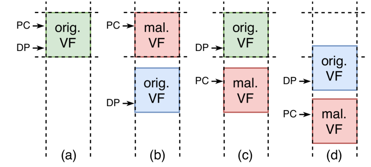
Memory copy attacks
Seshadri et al. [12] specify memory copy attacks that can be conducted by the adversary in the following three different ways as illustrated in Figure 7:
-
(b)
the adversary replaces the checksum function with an altered checksum function and executes it, but computes the checksum over a correct copy of the checksum function elsewhere in memory. Thus, the program counter is correct, but the data pointer points to the original copy of the checksum function in a different memory location.
-
(c)
the adversary uses the correct checksum function code in the original memory location to compute the checksum value, but executes a modified checksum function elsewhere in memory. Thus, the data pointer points to the original checksum function, but the program counter will be different.
-
(d)
the adversary places both the original checksum function code and its altered version elsewhere from the memory locations where the correct checksum code originally resided. Thus, both the program counter and the data pointer will be different compared to an execution of the original checksum function.
To prevent memory copy attacks, both the program counter and the data pointer need to be included in the computation of the checksum. The DP is included in each step of the computation, whereas the PC is indirectly included using self-modifying code. In addition to these specified attacks, the attacker could also move the entire checksum function to a different location in memory using a deep memory copy. This would modify the position of the checksum function in the memory, but not its functionality. Thus, this is not considered a memory copy attack.
Proxy attacks
We refer to proxy attacks as attacks where the adversary eavesdrops on the communication and obtains the challenge sent to the device, sends it to a proxy, computes the checksum function there and returns the result to the verifier. We distinguish between the following cases:
-
1.
other GPU on the same host: in case of a multi-GPU environment, we suggest to establish (and maintain) in sequence starting from the most powerful GPU to the least powerful one.
-
2.
other GPU on a different host: By involving a remote entity, the measured execution time will increase by the network latency for both sending the challenge and receiving the response. Tuning the number of checksum iterations to make the detection threshold smaller than the network latency, prevents using a more powerful GPU in a remote location. Furthermore, given that the verifier enclave frequently sends challenges and measures the execution time, this effect is amplified and thus would result in a noticeable difference with high probability [38].
TOCTOU attacks / Execution environment takeover
Time-of-check to time-of-use (TOCTOU) attacks [39] are caused by a race condition involving the checking of the state of a part of a system and the use of the results of that check. In SAGE, these attacks are considered because the checksum computation happens prior to the execution of the user kernel. In the particular, the adversary has two points where it could take over the execution environment set up by the VF: 1) before the launch of the user kernel, and 2) after the execution of the user kernel has completed. In the former case, the execution of the user kernel gets scheduled by the scheduler on the GPU. In case another kernel that is controlled by the adversary is present, this kernel could be scheduled instead of the user kernel. This is prevented by inlining the user kernel into the VF such that the epilog of the VF can directly call the user kernel using a function call. In the latter case, the execution of the user kernel has finished and thus the user is indifferent whether the dynamic root-of-trust has been compromised. If the user wants to execute another kernel, the dynamic RoT needs to be re-established.
Physical attacks
Our threat model considers physical attacks on the server. Consequently, the adversary could get physical access to the host and also the GPU memory, perform a memory dump, and analyze it to extract potential secrets. Unlike snooping and tampering off-package memory, local memory in a GPU package is considered to be much harder [40]. To increase the attack complexity of such physical attacks, the symmetric key established using SAKE is located in shared memory. Physical attacks on the host system are also possible and could include snooping on the PCIe bus or the host main memory. Since the host system is assumed to be untrusted (except for the verifier enclave and its related components), physical attacks on the host would allow similar attacks as in software.
8.1 Formal Verification of Modified SAKE
To show that our modified SAKE protocol securely establishes a key between the verifier and the GPU, we have formally modeled the key establishment protocol and verified its security properties using the Tamarin prover [41] under the assumption that the computed checksum provides a short-lived secret. To model this property in Tamarin, we use a single-use authentic channel over which we will send . We show that the established symmetric key remains secret and is unique, a weak agreement exists between the verifier and the device, and recent aliveness for each run of the protocol [42]. The proofs generated using the Tamarin prover can be found here https://github.com/spcl/sage/tree/main/proofs.
9 Related Work
Trusted execution on GPUs
To support trusted execution on GPUs, the following approaches were proposed. Graviton [4] specifies an architecture for supporting trusted execution environments on GPUs by changing the GPU’s command processor to perform remote attestation based on device specific keys and ensure isolation between multiple processes running on the GPU. This is achieved by utilizing a set of keys where the root key gets baked into device upon its creation. The latter requires modification to the GPU hardware by modifying the GPU’s internal command processor to impose a strict ownership discipline.
HIX [5] proposes a heterogeneous isolated execution environment. HIX does not require modifications to the GPU architecture to offer an isolated execution environment, but instead physically modifies the I/O interconnect between the CPU and GPU and refactors the GPU device driver to work from within a TEE on the host. The TEE can then allocate trusted enclaves on the GPU.
HETEE [6] is based on a standalone computing system to dynamically allocate accelerators (such as GPUs or FPGAs) for either secure computing, or available to the host OS using PCIe switches. The security controller (and its software) is assumed to be trusted and interacts with the management CPU to control PCIe switching. HETEE attempts to provide isolation by selectively making accelerators available to specific applications by controlling communication to the accelerator through the security controller.
Telekine [43] illustrates side-channel attacks against TEE on GPUs based on observing the timing of GPU kernel execution. It then introduces a GPU stream abstraction that ensures execution and interaction through untrusted components are independent of any secret data. Telekine requires a GPU TEE to be deployed.
Machine learning represents a major use case for using GPUs as accelerators and can require privacy-preserving approaches for sensitive data. Slalom [44] uses a combination of a trusted enclave and untrusted GPU. The system decomposes the machine learning into two parts, where the control flow part runs inside the trusted enclave and operations that are not privacy sensitive (such as convolutions based on matrix multiplications) are offloaded to the GPU. Unfortunately, the split results in a decrease of training and inference accuracy.
Software-based attestation
SWATT [13] uses a verification function that is based on pseudo-random memory traversal to a compute memory checksum. The verifier measures the execution time and verifies the checksum. Malicious code is required to verify each memory access to replace memory reads of changed locations with expected content, resulting in detectable time overhead. SWATT checks the entire memory of a system and its running time becomes prohibitive on systems with large memories.
PIONEER [12] verifies the integrity and guarantees the execution of code using a checksum function that is closely tied to the Pentium 4 architecture. The checksum function computes a fingerprint of the verification function and sets up an untampered execution environment. It is constructed such that manipulations by the adversary will noticeably increase the computation time.
Kovah et al. [45] and Butterworth et al. [46] extended the checksum computation to work on a Microsoft Windows system (CPU only), enabling a remote verifier to attest to a running system in a corporate environment.
Shaneck et al. [47] describe a software-based approach to remotely attest the static memory contents of sensors without requiring any additional hardware on the sensors nor precise measurements of execution timing. They use self-modifying code that generates memory read and jump instructions during the execution of their code.
Gligor and Woo [11] proposed a system that allows to provably establish a root of trust and provide secure initial states for all software unconditionally. The authors design a family of -independent (almost) universal hash functions based on polynomials and use Horner’s rule to show time- and memory-optimal evaluation of polynomials. Their proofs only hold under the unit time assumption in their concrete Word Random Access Machine (cWRAM) model. In addition, the proposed polynomials get very large for large number of words (computation time in the order of minutes).
10 Conclusion
The prospect of software-only trust root establishment and secure code execution on GPUs offers exciting opportunities: execution of sensitive GPU code that should not be leaked to the GPU operator (code secrecy), correct execution of GPU code in an adversarial environment (code and execution integrity), preserving data correctness and confidentiality in the presence of malicious code on the system (data secrecy and integrity). SAGE represents a first step for achieving these properties on the NVIDIA Ampere architecture, under the circumstances that the architectural details about the Ampere architecture are closed-source. Since architectural knowledge for designing the verification function (VF) is key, our software-based approach to provide secure code execution on GPU paves the way forward for GPU vendors: they are naturally in a position to align the design of the VF to their architectural knowledge and lead the standardization process for trust establishment on GPUs.
Remaining open challenges include the design of software-based secure execution on alternative platforms, improving the execution speed of the verification function, and extend the execution model to support libraries that use a hybrid CPU+GPU compute model (e.g., TensorFlow [48]). Ultimately, an interesting future research question to answer is the interplay between hardware- and software-based approaches for trusted execution to achieve the strongest possible security properties for GPU-based execution.
References
- [1] Markets and Markets, “Data center accelerator market - global forecast to 2026,” https://www.researchandmarkets.com/reports/5390148/data-center-accelerator-market-by-processor-type, 2021, [Online; accessed 01-Feb-2022].
- [2] V. Costan and S. Devadas, “Intel SGX explained,” IACR Cryptol. ePrint Arch., vol. 2016, no. 86, pp. 1–118, 2016.
- [3] ARM, “ARM trustzone technology,” https://developer.arm.com/ip-products/security-ip/trustzone, 2021, [Online; accessed 01-Feb-2022].
- [4] S. Volos, K. Vaswani, and R. Bruno, “Graviton: Trusted execution environments on GPUs,” in USENIX Symposium on Operating Systems Design and Implementation (OSDI), 2018, pp. 681–696.
- [5] I. Jang, A. Tang, T. Kim, S. Sethumadhavan, and J. Huh, “Heterogeneous isolated execution for commodity GPUs,” in Proceedings of the Twenty-Fourth International Conference on Architectural Support for Programming Languages and Operating Systems (ASPLOS), 2019, pp. 455–468.
- [6] J. Zhu, R. Hou, X. Wang, W. Wang, J. Cao, L. Zhao, F. Yuan, P. Li, Z. Wang, B. Zhao et al., “Enabling privacy-preserving, compute-and data-intensive computing using heterogeneous trusted execution environment,” arXiv preprint arXiv:1904.04782, 2019.
- [7] Nvidia, “Multi-instance GPU user guide,” https://docs.nvidia.com/datacenter/tesla/mig-user-guide/, 2021, [Online; accessed 01-Feb-2022].
- [8] ——, “How nvidia egx is forming central nervous system of global industries,” https://blogs.nvidia.com/blog/2020/05/15/egx-security-resiliency/, 2020, [Online; accessed 01-Feb-2022].
- [9] L. E. Olson, J. Power, M. D. Hill, and D. A. Wood, “Border control: Sandboxing accelerators,” in 48th Annual IEEE/ACM International Symposium on Microarchitecture (MICRO). IEEE, 2015, pp. 470–481.
- [10] TechSpot, “Intel’s sgx deprecation impacts drm and ultra hd blu-ray support,” https://www.techspot.com/news/93006-intel-sgx-deprecation-impacts-drm-ultra-hd-blu.html, 2022, [Online; accessed 01-Feb-2022].
- [11] V. D. Gligor and S. L. M. Woo, “Establishing software root of trust unconditionally.” in NDSS, 2019.
- [12] A. Seshadri, M. Luk, E. Shi, A. Perrig, L. Van Doorn, and P. Khosla, “Pioneer: verifying code integrity and enforcing untampered code execution on legacy systems,” in Proceedings of the ACM symposium on Operating systems principles, 2005, pp. 1–16.
- [13] A. Seshadri, A. Perrig, L. Van Doorn, and P. Khosla, “SWATT: Software-based attestation for embedded devices,” in IEEE Symposium on Security and Privacy (S&P), 2004, pp. 272–282.
- [14] J. Zhao, V. Gligor, A. Perrig, and J. Newsome, “Redabls: revisiting device attestation with bounded leakage of secrets,” in Cambridge International Workshop on Security Protocols, 2013, pp. 94–114.
- [15] Nvidia, “Int 32 and fp64 can be used concurrently in the volta architecture?” https://forums.developer.nvidia.com/t/int-32-and-fp64-can-be-used-concurrently-in-the-volta-architecture/108729/4, 2021, [Online; accessed 01-Feb-2022].
- [16] S. W. Keckler, W. J. Dally, B. Khailany, M. Garland, and D. Glasco, “Gpus and the future of parallel computing,” IEEE micro, vol. 31, no. 5, pp. 7–17, 2011.
- [17] R. Neugebauer, G. Antichi, J. F. Zazo, Y. Audzevich, S. López-Buedo, and A. W. Moore, “Understanding pcie performance for end host networking,” in Proceedings of the Conference of the ACM Special Interest Group on Data Communication, 2018, pp. 327–341.
- [18] Nouveau, “Accelerated open source driver for nVidia cards,” https://nouveau.freedesktop.org/, 2021, [Online; accessed 01-Feb-2022].
- [19] A. Seshadri, M. Luk, and A. Perrig, “Sake: Software attestation for key establishment in sensor networks,” in International Conference on Distributed Computing in Sensor Systems, 2008, pp. 372–385.
- [20] R. Anderson, F. Bergadano, B. Crispo, J.-H. Lee, C. Manifavas, and R. Needham, “A new family of authentication protocols,” ACM SIGOPS Operating Systems Review, vol. 32, no. 4, pp. 9–20, 1998.
- [21] Z. Jia, M. Maggioni, J. Smith, and D. P. Scarpazza, “Dissecting the NVIDIA Turing T4 GPU via microbenchmarking,” arXiv preprint arXiv:1903.07486, 2019.
- [22] Z. Jia, M. Maggioni, B. Staiger, and D. P. Scarpazza, “Dissecting the NVIDIA Volta GPU architecture via microbenchmarking,” arXiv preprint arXiv:1804.06826, 2018.
- [23] nVidia, “Basic linear algebra on nvidia gpus,” https://developer.nvidia.com/cublas, 2022, [Online; accessed 01-Feb-2022].
- [24] Nvidia, “CUDA binary utilities,” https://docs.nvidia.com/cuda/cuda-binary-utilities/index.html, 2021, [Online; accessed 01-Feb-2022].
- [25] ——, “Ampere architecture in-depth,” https://developer.nvidia.com/blog/nvidia-ampere-architecture-in-depth/, 2020, [Online; accessed 01-Feb-2022].
- [26] ——, “Cuda occupancy calculator,” https://docs.nvidia.com/cuda/cuda-occupancy-calculator/index.html, 2021, [Online; accessed 01-Feb-2022].
- [27] Intel, “Software guard extensions for Linux,” https://github.com/intel/linux-sgx, 2021, [Online; accessed 01-Feb-2022].
- [28] ——, “Interface for generic crypto library APIs required in SDK implementation,” https://github.com/intel/linux-sgx/blob/master/common/inc/sgx_tcrypto.h, 2021, [Online; accessed 01-Feb-2022].
- [29] Nvidia, “CUDA random number generation library,” https://docs.nvidia.com/cuda/curand/index.html, 2021, [Online; accessed 01-Feb-2022].
- [30] B. Forlin, R. Husemann, L. Carro, C. Reinbrecht, S. Hamdioui, and M. Taouil, “G-puf: An intrinsic puf based on GPU error signatures,” in IEEE European Test Symposium (ETS), 2020, pp. 1–2.
- [31] P. Van Aubel, D. J. Bernstein, and R. Niederhagen, “Investigating sram pufs in large cpus and gpus,” in International Conference on Security, Privacy, and Applied Cryptography Engineering, 2015, pp. 228–247.
- [32] A. Schaller, W. Xiong, N. A. Anagnostopoulos, M. U. Saleem, S. Gabmeyer, B. Škorić, S. Katzenbeisser, and J. Szefer, “Decay-based dram pufs in commodity devices,” IEEE Transactions on Dependable and Secure Computing, vol. 16, no. 3, pp. 462–475, 2019.
- [33] J. S. Teh, A. Samsudin, M. Al-Mazrooie, and A. Akhavan, “Gpus and chaos: a new true random number generator,” Nonlinear Dynamics, vol. 82, no. 4, pp. 1913–1922, 2015.
- [34] E. B. Smid, S. Leigh, M. Levenson, M. Vangel, D. Banks, A. Heckert, J. Dray, and S. Vo, “A statistical test suite for random and pseudorandom number generators for cryptographic applications,” 2010.
- [35] G. Marsaglia, “Diehard: a battery of tests of randomness,” http://stat.fsu.edu/geo, 1996.
- [36] J. Walker, “ENT - a pseudorandom number sequence test program,” https://www.fourmilab.ch/random/, 2008, [Online; accessed 01-Feb-2022].
- [37] Intel, “Xeon gold 6348 processor,” https://ark.intel.com/content/www/us/en/ark/products/212456/intel-xeon-gold-6348-processor-42m-cache-2-60-ghz.html, 2021, [Online; accessed 01-Feb-2022].
- [38] Y. Li, J. M. McCune, and A. Perrig, “VIPER: Verifying the integrity of peripherals’ firmware,” in Proceedings of the ACM Conference on Computer and Communications Security (CCS), 2011. [Online]. Available: /publications/papers/li_mccune_perrig_viper_ccs2011.pdf
- [39] I. De Oliveira Nunes, S. Jakkamsetti, N. Rattanavipanon, and G. Tsudik, “On the toctou problem in remote attestation,” in Proceedings of the 2021 ACM SIGSAC Conference on Computer and Communications Security, 2021, pp. 2921–2936.
- [40] E. Worthman, “Designing for security,” https://semiengineering.com/designing-for-security-2/, 2015, [Online; accessed 01-Feb-2022].
- [41] T. Team, “Tamarin prover,” https://tamarin-prover.github.io/, 2021, [Online; accessed 01-Feb-2022].
- [42] ——, “Tamarin manual - property specification,” https://tamarin-prover.github.io/manual/book/007_property-specification.html, 2021, [Online; accessed 01-Feb-2022].
- [43] T. Hunt, Z. Jia, V. Miller, A. Szekely, Y. Hu, C. J. Rossbach, and E. Witchel, “Telekine: Secure computing with cloud GPUs,” in 17th USENIX Symposium on Networked Systems Design and Implementation (NSDI), 2020, pp. 817–833.
- [44] F. Tramer and D. Boneh, “Slalom: Fast, verifiable and private execution of neural networks in trusted hardware,” arXiv preprint arXiv:1806.03287, 2018.
- [45] X. Kovah, C.Kallenberg, C. Weathers, A. Herzog, M. Albin, and J. Butterworth, “New results for timing-based attestation,” May 2012.
- [46] J. Butterworth, C. Kallenberg, X. Kovah, and A. Herzog, “BIOS chronomancy: fixing the core root of trust for measurement,” in Proceedings of ACM SIGSAC Conference on Computer and Communications Security (CCS), Nov. 2013.
- [47] M. Shaneck, K. Mahadevan, V. Kher, and Y. Kim, “Remote software-based attestation for wireless sensors,” in European Workshop on Security in Ad-hoc and Sensor Networks. Springer, 2005, pp. 27–41.
- [48] Tensorflow, “An end-to-end open source machine learning platform,” https://www.tensorflow.org/, 2021, [Online; accessed 01-Feb-2022].