TAPA: A Scalable Task-Parallel Dataflow Programming Framework for Modern FPGAs with Co-Optimization of HLS and Physical Design
Abstract.
In this paper, we propose TAPA, an end-to-end framework that compiles a C++ task-parallel dataflow program into a high-frequency FPGA accelerator. Compared to existing solutions, TAPA has two major advantages. First, TAPA provides a set of convenient APIs that allow users to easily express flexible and complex inter-task communication structures. Second, TAPA adopts a coarse-grained floorplanning step during HLS compilation for accurate pipelining of potential critical paths. In addition, TAPA implements several optimization techniques specifically tailored for modern HBM-based FPGAs. In our experiments with a total of 43 designs, we improve the average frequency from 147 MHz to 297 MHz (a 102% improvement) with no loss of throughput and a negligible change in resource utilization. Notably, in 16 experiments we make the originally unroutable designs achieve 274 MHz on average. The framework is available at https://github.com/UCLA-VAST/tapa and the core floorplan module is available at https://github.com/UCLA-VAST/AutoBridge.
1. Introduction
High-level synthesis (HLS) with the task-parallel programming model is an important tool to help programmers scale up the performance of their accelerators on modern FPGAs with ever-increasing resource capacities. Task-level parallelism is a form of parallelization of computer programs across multiple processors. In contrast to data parallelism where the workload is partitioned on data and each processor executes the same program (e.g., OpenMP (Dagum and Menon, 1998)), different processors in a task-parallel program often behave differently, while data are passed between processors. Examples of task-parallel programs include image processing pipelines (Pu et al., 2017; Chi et al., 2018a; Li et al., 2020), graph processing (Dai et al., 2016, 2017; Zhou et al., 2019; Wang et al., 2019) and network switching (Papaphilippou et al., 2020). Researches show that even for data-parallel applications like neural networks (Wang et al., 2021; Sohrabizadeh et al., 2020, 2022) and stencil computation (Chi et al., 2018a), task-parallel implementations show better scalability and higher frequency than their data-parallel counterparts due to the localized communication pattern (Cong et al., 2018a).
Even though task-parallel programs are suitable for spatial architectures, existing FPGA computer-aided design (CAD) toolchains still often fail in timing closure. One major cause that leads to the unsatisfactory frequency is that HLS cannot easily predict the physical layout of the design after placement and routing, thus HLS tools typically rely on pre-characterized operation delays and a very crude interconnect delay model to insert clock boundaries (i.e., registers) into an untimed design to generate a timed RTL implementation (Zheng et al., 2014; Tan et al., 2015; Guo et al., 2020). Hence, as the HLS designs get larger, the behavior-level estimation becomes even less accurate and the timing quality of the synthesized RTLs usually further degrades.
This timing issue is worsened as modern FPGA architectures become increasingly heterogeneous (Xilinx, 2020b). Modern FPGAs have thousands of heterogeneous digital signal processing (DSP) and random-access memory (RAM) blocks and millions of lookup table (LUT) and flip-flop (FF) instances. In order to pack more logic onto a single device, the latest FPGAs integrate multiple dies using silicon interposers, but the interconnects that go across the die boundaries would carry a non-trivial delay penalty. In addition, specialized IP blocks such as PCIe and DDR controllers are embedded in the programmable logic. These IP blocks usually have fixed locations near-dedicated I/O banks and will consume a large number of programmable resources nearby. As a result, these dedicated IPs often detour the signals close by towards more expensive and/or longer routing paths. This complexity and heterogeneity significantly challenge the effectiveness and efficiency of modern FPGA CAD workflow.
Moreover, the recent release of High Bandwidth Memory (HBM) based FPGA boards brings even more challenges to the timing closure of HLS designs. The key feature of the HBM device is that a super wide data interface is exposed in a local region, which often causes severe local congestion. For example, the AMD/Xilinx U280 FPGA features 32 independent HBM channels at the bottom of the device, each with a 256-bit width running at 450 MHz. To fully utilize the potential of the HBM bandwidth, the physical design tools need to squeeze a substantial amount of logic into the area nearby the HBM blocks.
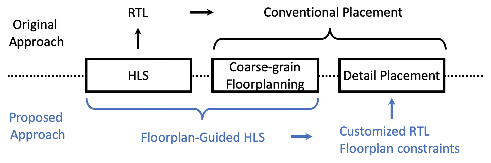
In this paper, we identify that the current timing-closure struggle originates from a disconnection between the HLS step and the downstream physical design step. The existing FPGA compilation stack consists of a sequence of independent design and optimization steps to gradually lower the design abstraction, but these steps lack cross-stack coordination and optimizations. Given a C++ task-parallel program input, HLS has the flexibility to adjust the output RTL to change the pipeline level of the inter-task data links, which are usually latency-insensitive; however, the tool does not know which ones will be timing critical. On the other hand, the physical design tools could determine the critical paths but no longer have the option to add extra registers because physical design tools honor the cycle-accurate RTL input.
Therefore, we propose to re-structure the CAD stack and partially combine physical design with HLS. Specifically, we propose to couple the coarse-grained floorplanning step with behavior-level pipelining in HLS. Our coarse-grained floorplanning involves dividing the FPGA device into a grid of regions and assigning each task to one region during HLS compilation. We further pipeline all the inter-region connections to facilitate timing closure while we leave the intra-region optimization to the default HLS tool. As our experiment will show, floorplanning a 4-die FPGA into only 6-8 regions is already enough to properly guide HLS for accurate elimination of global critical paths, thus our floorplan-guided HLS approach is lightweight and highly scalable.
Our methodology relieves local congestion and fixes global critical paths at the same time. First, the early floorplanning step could guide the subsequent placement steps to distribute the user logic evenly across the entire device instead of attempting to pack the logic into a single die as much as possible, which aims to alleviate local congestion as much as possible. Second, the floorplan provides HLS a view of the global physical layout which helps HLS accurately identify and pipeline the long wires, especially those crossing the die boundaries, so the global critical paths could be appropriately pipelined. Finally, we present analysis and latency balancing algorithms to guarantee that the throughput of the resulting design is not negatively impacted. Our contributions are as follows:
-
•
To the best of our knowledge, we are the first to tackle the challenge of high-frequency HLS design on multi-die FPGAs by coupling floorplanning and pipelining to effectively insert registers on the long cross-die interconnects. We further ensure that the additional latency does not affect the throughput of the design.
-
•
We present a set of optimizations specifically tailored for HBM devices, including automatic HBM port binding, floorplan solution space exploration, and a customized programming API to minimize the area overhead of HBM IO modules.
-
•
Our framework, TAPA, interfaces with the commercial FPGA design tool flow. It improves the average frequency of 43 designs from 147 MHz to 297 MHz with a negligible area overhead.
This paper extends the two prior publications (Guo et al., 2021; Chi et al., 2020) of the authors on this topic. Compared to the prior papers, this paper includes additional contributions as follows:
- •
- •
- •
-
•
We add four extra benchmarks that use a large number of HBM channels. We demonstrate how our new optimization enables them to be successfully implemented with high frequency (Section 7.4).
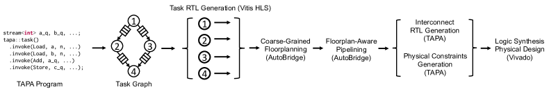
Figure 1 shows the overall flow of our proposed methodology. The rest of the paper is organized as follows: Section 2 introduces background information on modern FPGA architectures and shows motivating examples; Section 3 presents our proposed task-parallel programming model; Section 4 details our coarse-grained floorplan scheme inside the HLS flow; Section 5 describes our floorplan-aware pipelining methods; Section 6 elaborates our techniques tailored for HBM-based FPGAs; Section 7 presents experimental results; Section 8 provides related work, followed by conclusion and acknowledgements.
2. Background and Motivating Examples
2.1. High-Level Synthesis
The rapid increase of complexity in FPGA design has pushed the industry and academia to raise the design abstractions with better productivity than the register transfer level (RTL). High-level synthesis (HLS) plays a central role by enabling the automatic synthesis of high-level, untimed, or partially timed specifications (e.g. C++ or OpenCL) to low-level cycle-accurate RTL specifications for efficient implementation in the field programmable gate arrays (FPGAs) or application-specific integrated circuits (ASICs). The typical flow of modern FPGA HLS tools usually consists of three core steps: (1) scheduling, (2) binding, and (3) RTL generation.
-
•
The scheduling phase inserts clock boundaries into the original untimed specification. It takes in the control data flow graph (CDFG) generated by a compiler front-end from the high-level description (e.g., C/C++) and then maps the operations in the CDFG to the states and the control flow to state transitions specified by a finite-state machine (FSM). In each clock cycle, the controller would be in a state in the corresponding FSM.
-
•
The binding process maps high-level operations and variables to RTL-level resources, such as functional units and registers. It maps variables to registers and links wires from registers to functional units as operands of operations. The result of a functional unit is then wired to another functional unit or a register to store the computed value.
-
•
The RTL generation phase creates concrete RTL based on the results of the scheduling and the binding steps. The key in this step is to properly create the control logic to orchestrate the datapath, controlling each stage to execute at its scheduled cycle.
2.2. Task-Parallel Dataflow Programs
Task-level parallelism is a form of parallelization of computer programs across multiple processors. In contrast to data parallelism where the workload is partitioned on data and each processor executes the same program (e.g., OpenMP (Dagum and Menon, 1998)), different processors in a task-parallel program often behave differently, while data are passed between processors. For example, the multiple stages in an image processing pipeline (Pu et al., 2017; Chi et al., 2018a; Li et al., 2020) can each be implemented in a different processor. Task-parallel programs are often described using dataflow models (Hoare, 1978; Kahn, 1974; Lee and Messerschmitt, 1987a; Buck, 1993; Peterson, 1977), where tasks are called processes. Processes communicate only through unidirectional channels. Data exchanged between channels are called tokens. In this paper, we borrow the terms channel and token, and focus on the problem of statically mapping tasks to hardware. That is, instances of tasks are synthesized to different areas in an FPGA accelerator.
2.3. Multi-Die FPGA Architectures
Figure 2 shows three representative multi-die FPGA architectures, each of which is described in more detail as follows.
-
•
The Xilinx Alveo U250 FPGA is one of the largest FPGAs with four dies. All the I/O banks are located in the middle column and the four DDR controller IPs are positioned vertically in a tall-and-slim rectangle in the middle. On the right lies the Vitis platform region (Xilinx, 2020c), which incorporates the DMA IP, the PCIe IP, etc, and serves to communicate with the host CPU.
-
•
The Xilinx Alveo U280 FPGA is integrated with the latest High-Bandwidth Memory (HBM) (Choi et al., 2020, 2021; Xilinx-HBM, 2020), which exposes 32 independent memory ports at the bottom of the chip. I/O banks are located in the middle columns. Meanwhile, there is a gap region void of programmable logic in the middle.
-
•
The Intel Stratix 10 FPGA (Intel, 2020) also sets the DDR controller and I/O banks in the middle of the programmable logic. The embedded multi-die interconnect bridges and the PCIe blocks are distributed at the two sides of the chip, allowing multiple FPGA chips to be integrated together. Although this paper uses the Xilinx FPGAs to demonstrate the idea, our methodology is also applicable to Intel FPGAs and other architectures.
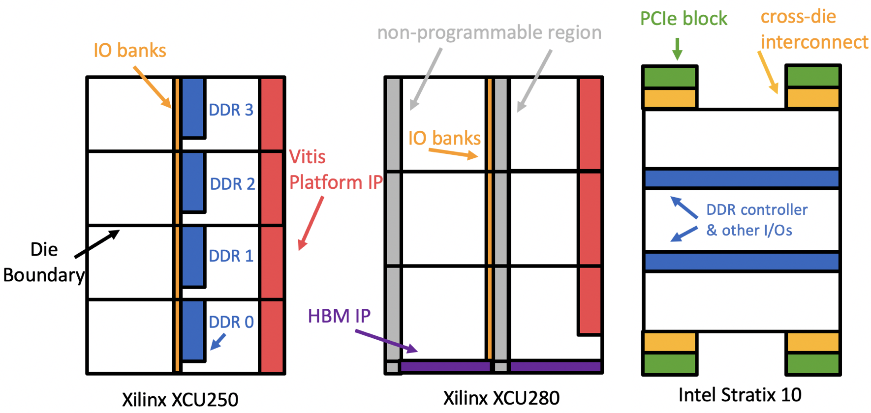
Compared to previous generations, the latest multi-die FPGA architectures are divided into disjoint regions, where the region-crossing naturally incurs additional signal delay. In addition, the large pre-located IPs consume significant programmable resources near their fixed locations which may also cause local routing congestion. These characteristics can hamper the existing HLS flows from achieving a high frequency.
2.4. Motivating Examples
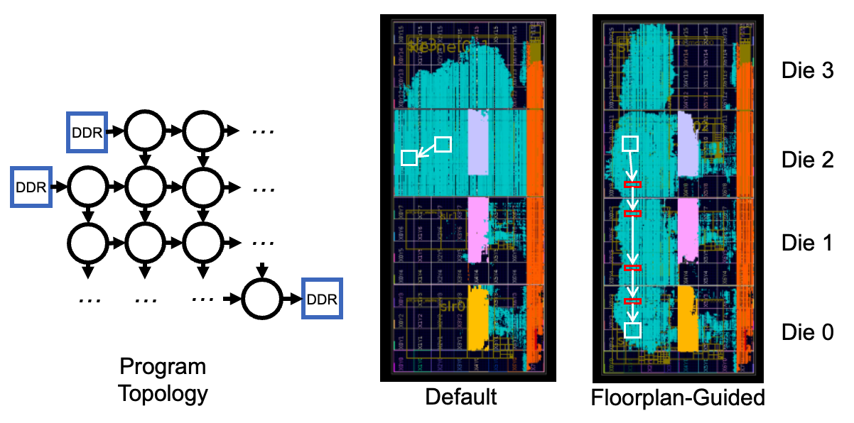
We show two examples to motivate our floorplan-guided HLS approach. First, Figure 3 shows a CNN accelerator implemented on the Xilinx U250 FPGA. It interacts with three DDR controllers, as marked in grey, pink, and yellow blocks in the figure. In the original implementation result, the whole design is packed close together within die 2 and die 3. To demonstrate our proposed idea, we first manually floorplan the design to distribute the logic in four dies and to avoid overlapping the user logic with DDR controllers. Additionally, we pipeline the FIFO channels connecting modules in different dies as demonstrated in the figure. The manual approach improves the final frequency by 53%, from 216 MHz to 329 MHz.
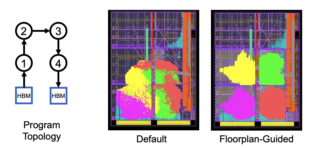
Second, Figure 4 shows a stencil computation design on the Xilinx U280 FPGA. It consists of four identical tasks in linear topology with each color representing a kernel. In the original implementation, the tool’s choice of die-crossing wires is sub-optimal and one kernel may be divided among multiple regions. Instead in our approach, we pre-determine all the die-crossing wires during HLS compilation and pipeline them, so the die boundaries will not cause problems for the placement and routing tool. For this example, we achieve 297 MHz while the design is originally unroutable.
3. Programming Model and Interfaces
In this section, we present the detailed task-programming model of TAPA and the user interfaces.
3.1. Basic Concepts
TAPA dataflow programs explicitly decouple communication and computation. A TAPA program has two types of building blocks: streams and tasks. A stream will be mapped to a FIFO in hardware; a task consumes data from input streams, performs arbitrary computation, then produces data into other output streams. All tasks execute in parallel and communicate with each other through streams.
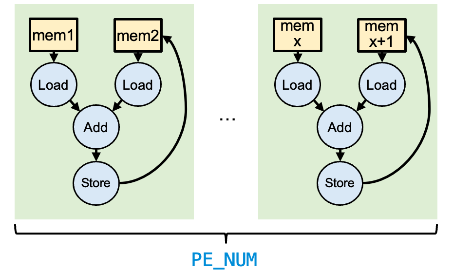
Listing 5 shows an example TAPA program that instantiates PE_NUM kernels and each kernel loads two vectors from external memory, adds them up, and stores the results back into external memory. The VecAdd function instantiates the three lower-level tasks and defines the communication streams between them. It takes 3 arguments: 3 mmap interfaces for the 3 vectors and one scalar for the vector length. 3 communication streams are defined in VecAdd. The 3 lower-level tasks are instantiated 4 times in total because there are 2 input vectors, each of which needs its own Load. The VecAdd function is an upper-level task. It is also the top-level task that defines the interface between the kernel and the host. Once the 4 children task instances are instantiated, they will run in parallel and their parent will wait until all children finish.
3.2. Hierarchical Programming Model
TAPA uses a hierarchical programming model. Each task is either a leaf that does not instantiate any streams or tasks, or a collection of tasks and streams with which the tasks communicate. A task that instantiates a set of tasks and streams is called the parent task for that set. Correspondingly, the instantiated tasks are the children tasks of their parent, which may be parents of their own children. Each stream must be connected to exactly two tasks. One of the tasks must act as a producer and the other must act as a consumer. Meanwhile, each task could connect to an arbitrary number of streams. The producer streams tokens to the consumer via the stream in the first-in-first-out (FIFO) order. Each task is implemented as a C++ function, which can communicate with each other via the communication interface. A parent task instantiates streams and tasks using the instantiation interface and waits until all its child tasks finish. One of the tasks is designated as the top-level task, which defines the communication interfaces external to the FPGA accelerator, i.e., the system integration interface.
3.3. Convenient Programming Interfaces
3.3.1. Communication Interface
TAPA provides separate communication APIs for the producer side and the consumer side, which use ostream and istream as the interfaces, respectively. The producer of a stream can test the fullness of the stream and append tokens to the stream (write) if the stream is not full. The consumer of a stream can test the emptiness of the stream and remove tokens from the stream (destructive read), or duplicate the head token without removing it (non-destructive read, a.k.a., peek), if the stream is not empty. Read, peek, and write operations can be blocking or non-blocking.
A special token denoting end-of-transaction (EoT) is available to all streams. A process can “close” a stream by writing an EoT token to it, and a process can “open” a stream by reading an EoT token from it. A process can also test if a stream is closed, which is a non-destructive read operation to the stream (eot). An EoT token does not contain any useful data. This is designed deliberately to make it possible to break from a pipelined loop when an EoT is present, for example, in Line LABEL:lln:eot_tapa of Listing 7. Listing 7 shows an example of how the communication interfaces are used.
3.3.2. Instantiation Interface
A parent task can instantiate streams using stream<type,capacity>. For example, stream<Pkt,2> instantiates a stream with capacity 2, and data tokens transmitted using this stream have type Pkt. Tasks are instantiated using task::invoke, with the first argument being the task function and the rest of the arguments being the arguments to the task instance. This is consistent with std::invoke in the C++ standard library.
3.3.3. Detached Tasks
Sometimes making the termination of the program dependent on each kernel function is overkill. For example, a task function may be purely data-driven and we do not have to terminate it on program termination. In that case, TAPA allows users to detach a task on invocation instead of joining it to the parent through the task().invoke<detach>() API. Such tasks can keep running forever as long as input data is available, and the central controller will not check if it is finished or not to determine the termination of the program.
3.3.4. System Integration Interface
TAPA uses a unified system integration interface to further reduce programmers’ burden. To offload a kernel to an FPGA accelerator, programmers only need to call the top-level task as a C++ function in the host code. Since TAPA can extract metadata information, e.g., argument type, from the kernel code, TAPA will automatically synthesize proper OpenCL host API calls and emit an implementation of the top-level task C++ function that can set up the runtime environment properly. As a user of TAPA, the programmer can use a single function invocation in the same source code to run software simulation, hardware simulation, and on-board execution, with the only difference of specifying proper kernel binaries.
3.4. Asynchronous External Memory Access
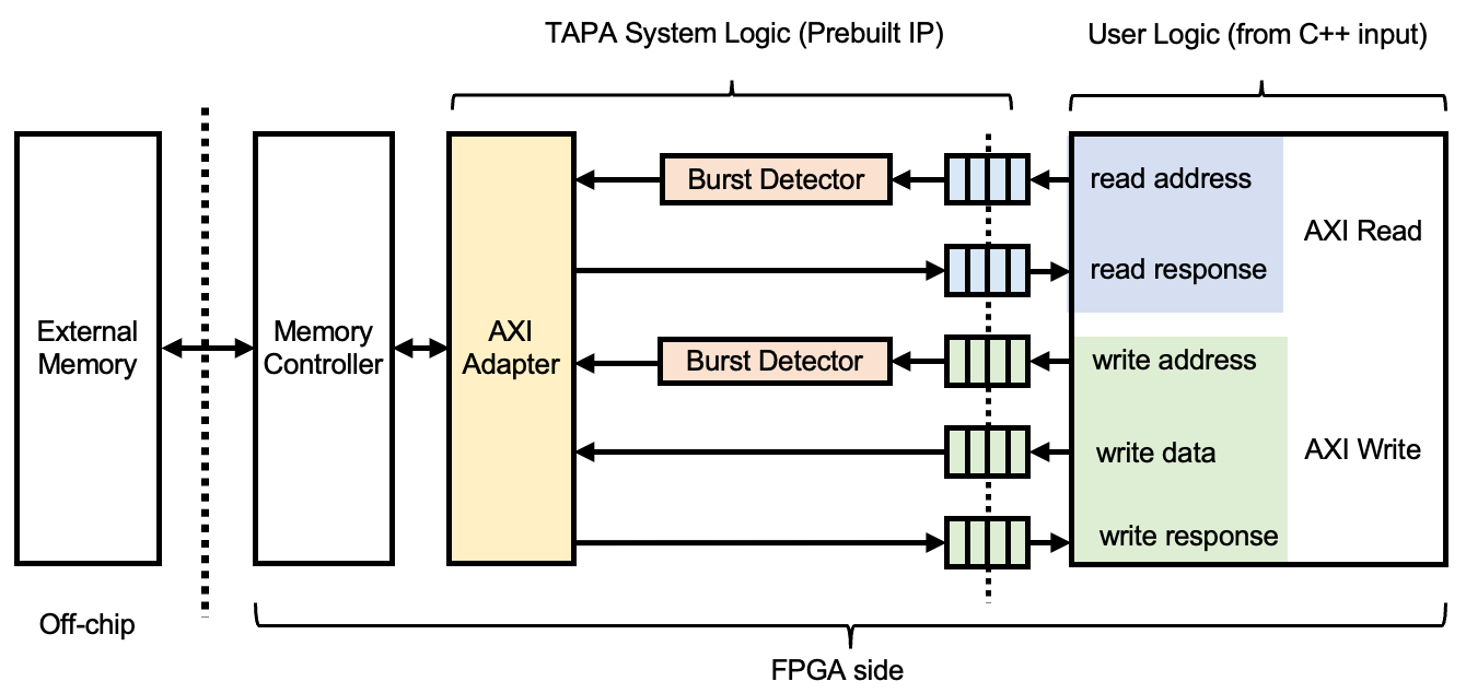
In order to provide users with more flexibility in accessing the external memory and to reduce the area overhead, we develop the async_mmap API. The async_mmap object represents an AXI channel as five independent streams, as shown in Figure 8. To read from an HBM channel, the user only needs to write out the target addresses one by one into the read_addr stream. The received data will be directly streamed to the user logic through another stream interface. Figure 9 shows an example of a sequential read operation. Likewise, to write data out into external memory, the user only needs to push the individual addresses and data to the write_addr channel.
Contrary to existing HLS solutions that infer burst transactions at the compile time through static analysis, we implement a runtime burst detection mechanism. The burst detector module will inspect the input addresses and merge sequential reads or writes into a longer burst transaction. Table 1 demonstrates the behavior of the burst detector. The input side is always available to accept new input addresses as long as the downstream AXI adapter is not congested. Internally, the burst detector will keep track of the longest stream of sequential addresses it has seen so far. Once a new input address is not consequential to the previous address, the burst detector will conclude the last transaction and produce a burst transaction to the output. Meanwhile, it will update the starting address of the next burst. In the case that the next input address is not available above a threshold, the burst detector will also conclude and issue out the current burst. The burst detector ensures that memory access will be as efficient as inferring burst transactions statically.
| Cycle | 0 | 1 | 2 | 3 | 4 | 5 | 6 | 7 | … | |
|---|---|---|---|---|---|---|---|---|---|---|
| Input | Read Requests | 64 | 65 | 66 | 67 | 128 | 129 | 130 | 256 | … |
| Ouput | AXI Read Addr | 64 | 128 | |||||||
| AXI Burst Len | 4 | 3 | ||||||||
| Internal State | Base Addr | 64 | 64 | 64 | 64 | 128 | 128 | 128 | 256 | |
| Length Counter | 1 | 2 | 3 | 4 | 1 | 2 | 3 | 1 | ||
The async_mmap API gives HLS users a similar level of fine-grained control of the RTL level. Users can use one dedicated task to issue read requests and another task to receive the read responses, which is hardly feasible in the common approach that abstracts the external memory as an array.
3.5. Overall Compilation Steps
Figure 1 shows the overall compilation flow. Given an input TAPA program, the tool will compile the top function into RTL and then invoke an existing HLS tool to compile each individual task. For the top function, the tool will analyze and extract how the tasks are interconnected and construct a task graph. The task graph will be used by the floorplan tools to assign each task to one region of the device and determine the pipeline level of each stream. The details of the floorplan process will be discussed in the following sections.
4. Coupling HLS with Coarse-Grained Floorplanning
In this section, we present our coarse-grained floorplanning scheme that assigns TAPA tasks to different regions of the programmable fabric.
Note that the focus of this work is not on improving floorplanning algorithms; instead, we intend to properly use coarse-grained floorplan information to guide HLS and placement.
4.1. Coarse-Grained Floorplanning Scheme
Instead of finding a dedicated region with a detailed aspect ratio for each module, we choose to view the FPGA device as a grid that is formed by the die boundaries and the large IP blocks. These physical barriers split the programmable fabric apart into a series of disjoint slots in the grid where each slot represents a sub-region of the device isolated by die boundaries and IP blocks. Using our coarse-grained floorplanning, we will assign each function of the HLS design to one of these slots.
For example, for the Xilinx Alveo U250 FPGA, the array of DDR controllers forms a vertical split in the middle column; and there are three horizontal die boundaries. Thus the device can be viewed as a grid of 8 slots in 2 columns and 4 rows. Similarly, the U280 FPGA can be viewed as a grid of 6 slots in 2 columns and 3 rows.
In this scheme, each slot contains about 700 BRAM_18Ks, 1500 DSPs, 400K Flip-Flops and 200K LUTs. Meanwhile, to reduce the resource contention in each slot, we set a maximum utilization ratio for each slot to guarantee enough blank space. Experiments show that such slot sizes are suitable, and HLS has a good handle on the timing quality of the local logic within each slot, as shown in Section 7.
4.2. Problem Formulation
Given: (1) a graph representing the task-parallel program where represents the set of tasks and represents the set of streaming channels between vertices; (2) the number of rows and the number of columns of the grid representation of the target device; (3) maximum resource utilization ratios for each slot; (4) location constraints such that certain IO modules must be placed nearby certain IP blocks. In addition, we may have constraints that certain vertices must be assigned to the same slot. This is for throughput concerns and will be explained in Section 5.
Goal: Assign each to one of the slots such that (1) the resource utilization ratio111Based on the estimation of resource utilization by HLS. We can increase the accuracy of the area estimation by optionally running logic synthesis of each task in parallel. of each slot is below the given limit; (2) the cost function is minimized. We choose the total number of slot-crossings as the cost instead of the total estimated wire lengths. Specifically, the cost function is defined as
| (1) |
where is the bitwidth of the FIFO channel connecting and and module is assigned to the -th column and the -th row. The physical meaning of the cost function is the sum of the number of slot boundaries that every wire crosses.
4.3. Solution
Our problem is relatively small in size as the number of tasks in behavior-level task parallel programs (typically less than thousands) is much smaller than the number of gates in a logic netlist. We adopt the main idea of top-down partitioning-based placement algorithms (Breuer, 1977; Dunlop et al., 1985; Maidee et al., 2003) to solve our problem. Meanwhile, due to the relatively small problem size, we plan to pursue an exact solution for each partitioning process.
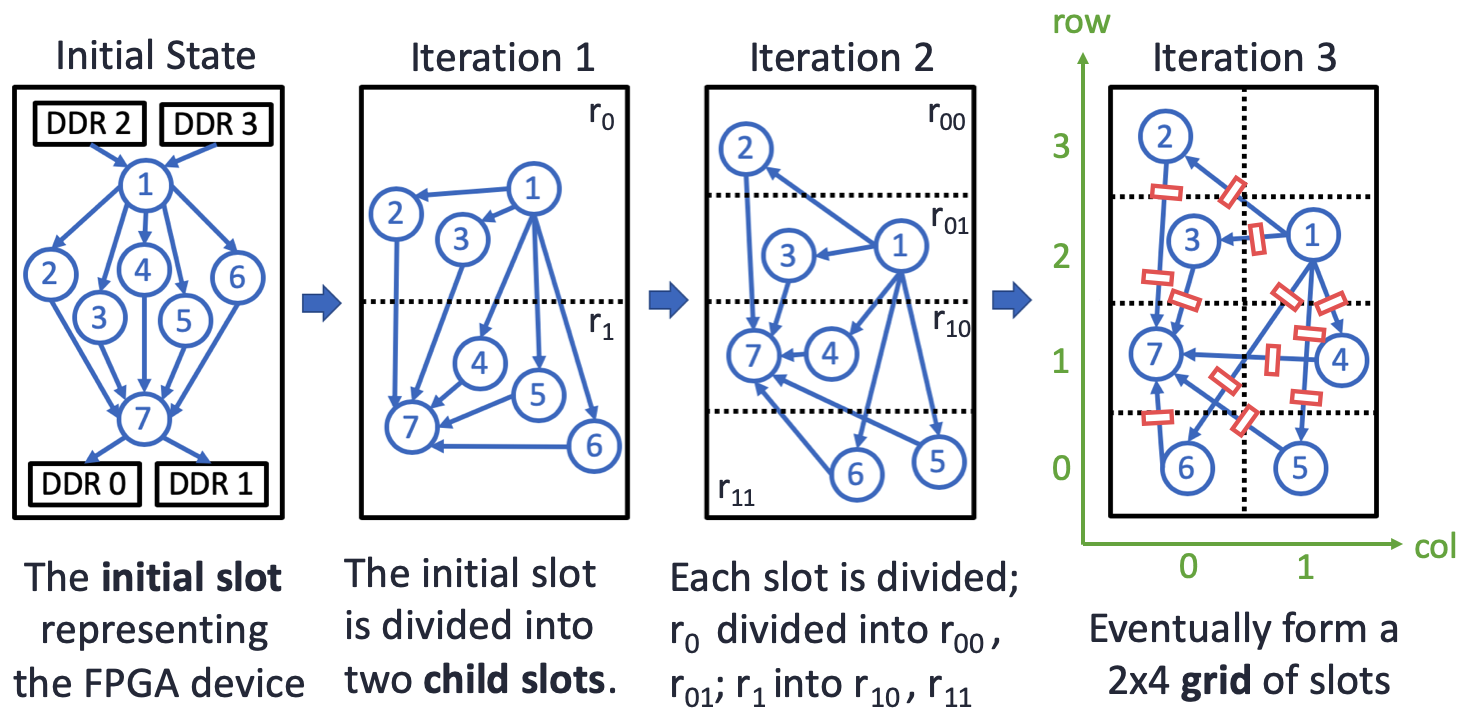
Figure 12 demonstrates the floorplanning of an example design through three iterations of partitioning. The top-down partitioning-based approach starts with the initial state where all modules are assigned to the same slot, iteratively partitions the current slots in half into two child slots and then assigns the modules into the child slots. Each partitioning involves splitting all of the current slots in half either horizontally or vertically.
We formulate the partitioning process of each iteration using integer linear programming (ILP). In every partitioning iteration, all current slots need to be divided in half. Since some of the modules in a slot may be tightly connected to modules outside of the slot, ignoring such connections can adversely affect the quality of the assignment. Therefore our ILP formulation considers the partitioning of all slots together for an exact solution which is possible due to the small problem size. Experiments in Section 7 show that our ILP formulation is solvable within a few seconds or minutes for designs of hundreds of modules.
Performing an N-way partitioning is another potential method. However, compared to our iterative 2-way partitioning, experiments show that it is much slower than iterative 2-way partitioning.
ILP Formulation of One Partitioning Iteration.
The formulation declares a binary decision variable for each to denote whether is assigned to the left or the right child slot during a vertical partitioning (or to the upper or the lower child slot for a horizontal one). Let denote the set of all current slots. For each slot to be divided, we use to denote the set of all vertices that is currently accommodating. To ensure that the child slots have enough resources for all modules assigned to them, the ILP formulation imposes the resource constraint for each child slot and for each type of on-chip resource.
| (2) |
where is the resource requirement of and represents the available resources in the child slot divided from .
To express the cost function that is based on the coordinates of each module, we first need to express the new coordinates of based on the previous coordinates and the decision variable . For a vertical partitioning, the new coordinates of will be
| (3) |
| (4) |
And for horizontal partitioning, the new coordinates will be
| (5) |
| (6) |
Finally, the objective is to minimize the total slot-crossing shown in Formula (1) for each partitioning iteration.
For the example in Figure 12, Table 2 shows the and indices of selected vertices in each partitioning iteration.
| Init | row = 0; col = 0 | |||||||||||
|---|---|---|---|---|---|---|---|---|---|---|---|---|
| iter-1 |
|
|
||||||||||
| iter-2 |
|
|
|
|
||||||||
| iter-3 |
|
|
||||||||||
5. Floorplan-Aware Pipelining
Based on the generated floorplan, we aim to pipeline every cross-slot connection to facilitate timing closure. Although HLS has the flexibility to pipeline them to increase the final frequency, the additional latency could potentially lead to a large increase of the execution cycles, which we need to avoid. This section presents our methods to pipeline slot-crossing connections without hurting the overall throughput of the design.
We will first focus on pipelining the dataflow designs, then extend the method to other types of HLS design. In Section 5.1 we introduce our approach of pipelining with latency balancing; and Section 5.2 presents the detailed algorithm. In Sections 5.3 we present how to utilize the internal computation pattern to construct loop-level dataflow graphs that allow more pipelining opportunities.
5.1. Pipelining Followed by Latency Balancing for Dataflow Designs
In our problem, an HLS dataflow design consists of a set of concurrently executed functions communicating through FIFO channels, where each function will be compiled into an RTL module controlled by a finite-state machine (FSM) (Peng and Puroshothaman, 1991). The rich expressiveness of FSM makes it difficult to statically determine how the additional latency will affect the total execution cycles. Note that our problem is different from other simplified dataflow models such as the Synchronous Data Flow (SDF) (Lee and Messerschmitt, 1987b) and the Latency Insensitive Theory (LIT) (Carloni et al., 2001), where the firing rate of each vertex is fixed. Unlike SDF and LIT, in our problem, each vertex is an FSM and the firing rate is not fixed and can have complex pattern.
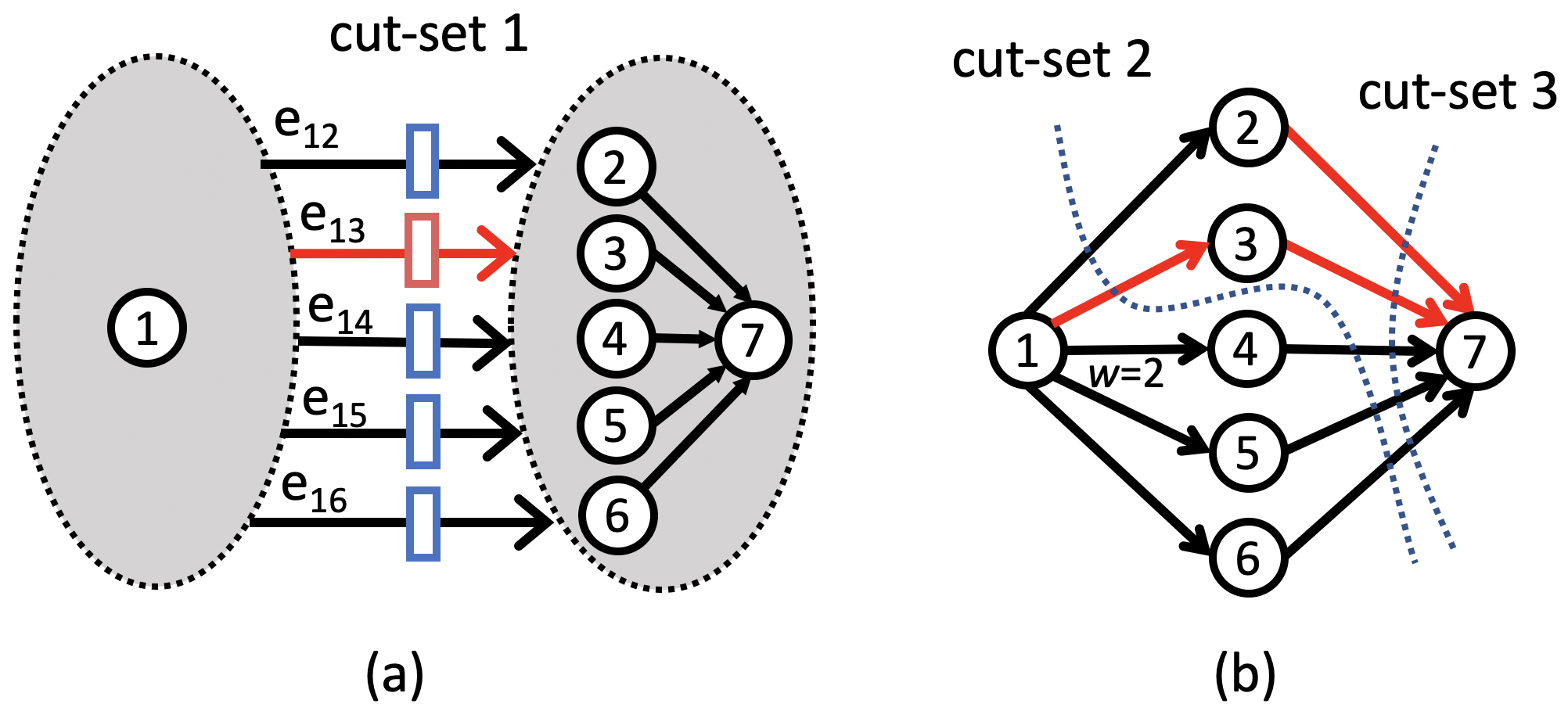
Therefore, we adopt a conservative approach, where we first pipeline all edges that cross slot boundaries, then balance the latency of parallel paths based on the cut-set pipelining (Parhi, 2007). A cut-set is a set of edges that can be removed from the graph to create two disconnected sub-graphs; and if all edges in a cut-set are of the same direction, we could add an equal amount of latency to each edge and the throughput of the design will be unaffected. Figure 13 (a) illustrates the idea. If we need to add one unit of latency to (marked in red) due to the floorplan results, we need to find a cut-set that includes and balance the latency of all other edges in this cut-set (marked in blue).
Since we can choose different cut-set to balance the same edge, we need to minimize the area overhead. For example, for , balancing the cut-set 2 in Figure 13 (b) costs smaller area overhead compared to cut-set 1 in Figure 13 (a), as the width of is smaller than that of . Meanwhile, it is possible that multiple edges can be included in the same cut-set. For example, the edges and are both included in the cut-set 3, so we only need to balance the other edges in cut-set 3 once.
Cut-set pipelining is equivalent to balancing the total added latency of every pair of reconvergent paths (Parhi, 2007). A path is defined as one or multiple concatenated edges of the same direction; two paths are reconvergent if they have the same source vertex and destination vertex. When there are multiple edges with additional latency from the floorplanning step, we need to find a globally optimal solution that ensures all reconvergent paths have a balanced latency, and the area overhead is minimized.
5.2. Latency Balancing Algorithm
Problem Formulation.
Given: A graph representing a dataflow design that has already been floorplanned and pipelined. Each vertex represents a function in the dataflow design and each edge represents the FIFO channel between functions. Each edge is associated with representing the bitwidth of the edge. For each edge , the constant represents the additional latency inserted to in the previous pipelining step. We use the integer variable to denote the number of latency added to in the current latency balancing step.
Goal: (1) For each edge , compute such that for any pair of reconvergent paths , the total latency on each path is the same:
and (2) minimize the total area overhead, which is defined as:
Note that this problem is different from the classic min-cut problem (Minimum-Cut, 2020) for DAG. One naïve solution is to find a min-cut for every pipelined edge, and increase the latency of the other edges in the cut accordingly. However, this simple method is suboptimal. For example in Figure 13, since edge and can be in the same cut-set, we only need to add one unit of latency to the other edges in the cut-set (e.g., , and ) so that all paths are balanced.
Solution.
We formulate the problem in a restricted form of ILP that can be solved in polynomial time. For each vertex , we associate it with an integer variable that denotes the maximum latency from pipelining between and the sink vertex of the graph. In other words, given two vertices and , represents the maximum latency among all paths between the two vertices. Note that we only consider the latency on edges due to pipelining.
For each edge , we have
According to our definition, the additional balancing latency added to edge in this step can be expressed as
since we want every path from to have the same latency.
The optimization goal is to minimize the total area overhead, i.e. the weighted sum of the additional depth on each edge:
For example, assume that there are two paths from to where path has 3 units of latency from pipelining while has 1 unit. Thus from our formulation, we will select the edge(s) on and add 2 additional units of latency to balance the total latency of and so that the area overhead is minimized.
Our formulation is essentially a system of differential constraints (SDC), in which all constraints are in the form of , where is a constant and are variables. Because of this restrictive form of constraints, we can solve SDC as a linear programming problem while the solutions are guaranteed to be integers. As a result, it can be solved in polynomial time (Leiserson and Saxe, 1991; Cong and Zhang, 2006).
If the SDC formulation does not have a solution, there must be a dependency cycle in the dataflow graph (Cong and Zhang, 2006). This means that at least one of the edges in the dependency cycle are pipelined based on the floorplan. In this situation, we will feedback to the floorplanner to constrain those vertices into the same region and then re-generate a new floorplan.
5.3. Efficient Pipelining Implementation
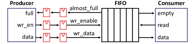
Figure 14 shows how we add pipelining to a FIFO-based connection. We adopt FIFOs that assert their full pin before the storage actually runs out, so that we could directly register the interface signals without affecting the functionality.
6. Optimization for HBM Devices
As will be shown in our evaluation section, the techniques from previous sections will already be effective for a significant timing improvement on DDR-based FPGAs. However, more optimization techniques are needed to squeeze the best performance out of the state-of-the-art HBM-based FPGAs. In this section, we present three major techniques tailored for the unique architecture of HBM-based FPGAs where a large set of independent data channels are clustered closely at the edge of the device.
6.1. Reduce BRAM Usage with async_mmap
First, we present a system-level optimization to reduce the resource consumption near the HBM blocks by using the async_mmap API presented in Section 3.4. When interacting with the AXI interface, existing HLS tools will buffer the entire burst transactions using on-chip memories. For a 512-bit AXI interface, the AXI buffers generated by Vitis HLS costs 15 BRAM_18K each for the read channel and the write channel. While this is trivial for conventional DDR-based FPGAs where only a few external DDRs are available, such BRAM overhead becomes a huge problem for HBM devices. To use all 32 HBM channels, the AXI buffers alone take away more than 900 BRAM_18Ks, which accounts for more than 70% of the BRAM resources in the bottom SLR.
However, with the async_mmap interface, we no longer need to set aside a large buffer to accommodate the data in AXI burst transactions, because the flow control mechanism is explicitly included in the user code (Figure 10). Table 3 shows our resource reduction for just one HBM channel.
| Interface | MHz | LUT | FF | BRAM | URAM | DSP |
|---|---|---|---|---|---|---|
| Vitis HLS Default | 300 | 1189 | 3740 | 15 | 0 | 0 |
| async_mmap | 300 | 1466 | 162 | 0 | 0 | 0 |
6.2. Automatic HBM Channel Binding
In the current FPGA HBM architecture, the HBM is divided into 32 channels are physically bundled into eight groups and each group contains four adjacent channels joined by a built-in 44 crossbar. The crossbar provides full connectivity within the group. Meanwhile, each AXI interface at the user side can still access any HBM channels outside its group. The data will sequentially traverse through each of the lateral connections until it reaches the crossbar connecting to the target channel, thus inter-group accesses will come with longer latency and potentially less bandwidth due to data link sharing. Therefore, the binding of logical buffers and physical HBM channels will affect the design in two ways:
-
•
Since intra-group access is more efficient compared to inter-group accesses, an inferior binding will negatively affect the available bandwidth.
-
•
As the HBM channels are hardened to fixed locations, the binding also affects the placement and routing of the logic that connect to HBM. Thus an unoptimized binding may cause local congestion in the programmable logic nearby the HBM channels.
Existing CAD tools require that users explicitly specify the mapping of all HBM channels, which requires users to master low-level architecture details. Also, since the binding does not affect the correctness of the design, users are often unaware of suboptimal choices.
To alleviate the problem, we propose a semi-automated solution. We observe that very often the design only involves intra-group HBM accesses. In this case, the binding decision does not affect the HBM bandwidth and latency and only impacts the placement and routing of nearby logic. Therefore, we implement an API where users could specify the partial binding of channels, or none at all if desired, and let TAPA automatically determines the binding for the rest.
Specifically, we incorporate the HBM binding process into our floorplanning step. We treat the number of available HBM channels as another type of resource for the slots. Therefore, slots that are directly adjacent to HBM blocks will be treated as having the corresponding number of HBM channels, while other slots will have zero available HBM channel resources. Meanwhile, each task that directly interacts with the HBM channel is treated as requiring one unit of HBM channel resources, and other tasks will be regarded as not requiring HBM resources.
6.3. Generating Multiple Floorplan Candidates
By default, TAPA will only generate one floorplan solution where we will prioritize a balanced distribution of logic and then accordingly pipeline the inter-slot connections. However, due to the severe local congestion around the bottom die in an HBM device, we need to explore the different trade-offs between logic resource usage and routing resource usage, especially die-crossing wires. One floorplan solution may use fewer logic resources in the bottom die but requires more die-crossing wires as logic are pushed to the upper regions; another solution may have the opposite effect. We observe that very often it is unpredictable which factor is more important for a given design until the routing process is done. Note that each different floorplan solution comes with corresponding pipelining schemes that best suit the floorplan results.
Instead of generating only one floorplan solution, we can generate a set of Pareto-optimal points and run physical design concurrently to explore the best results. In our formulation of the floorplan problem, we have a parameter to control the maximal logic resource utilization of each island. Reducing this parameter will reduce local logic resource usage and increase global routing resource usage and vice versa. Therefore, we sweep through a range of this parameter to generate a set of slightly different floorplans and implement them in parallel to achieve the highest frequency.
7. Experiments
7.1. Implementation Details
TAPA is implemented in C++ and Python. We implement our prototype to interface with the CAD flow for AMD/Xilinx FPGAs, including Vitis HLS, Vivado and Vitis (2021.2). We use the Python MIP package (Santos and Toffolo, 2020) coupled with Gurobi (Gurobi, 2020) to solve the various ILP problems introduced in previous sections. We generate tcl constraint files to be used by Vivado to enforce our high-level floorplanning scheme.
Meanwhile, we turn off the hierarchy rebuild process during RTL synthesis (Xilinx, 2020a) to prevent the RTL synthesis tool from introducing additional wire connections between RTL modules. The hierarchy rebuild step first flattens the hierarchy of the RTL design and then tries to rebuild the hierarchy. As a result, hierarchy rebuild may create unpredictable new connections between modules. As a result, if two modules are floorplanned far apart, these additional wires introduced during RTL synthesis will be under-pipelined as they are unseen during HLS compilation. Note that disabling this feature may lead to slight differences in the final resource utilization.
We test out designs on the Xilinx Alveo U250 FPGA222The U250 FPGA contains 5376 BRAM18K, 12288 DSP48E, 3456K FF and 1728K LUT with 4 DRAMs and the Xilinx Alveo U280 FPGA333The U280 FPGA contains 4032 BRAM18K, 9024 DSP48E, 2607K FF and 434K LUT with High-Bandwidth Memory (HBM). As the DDR controllers are distributed in the middle vertical column while the HBM controller lies at the bottom row, these two FPGA architectures present different challenges to the CAD tools. Thus it is worthwhile to test them separately.
To run our framework, users first specify how they want to divide the device. By default, we divide the U250 FPGA into a 2-column 4-row grid and the U280 FPGA into a 2-column 3-row grid, matching the block diagram of these two architectures shown in Figure 2. To control the floorplanning, users can specify the maximum resource utilization ratio of each slot. The resource utilization is based on the estimation by HLS. Users can also specify how many levels of pipelining to add based on the number of boundary crossings. By default, for each boundary crossing we add two levels of pipelining to the connection. The processed design is integrated with the Xilinx Vitis infrastructure to communicate with the host.
7.2. Benchmarks
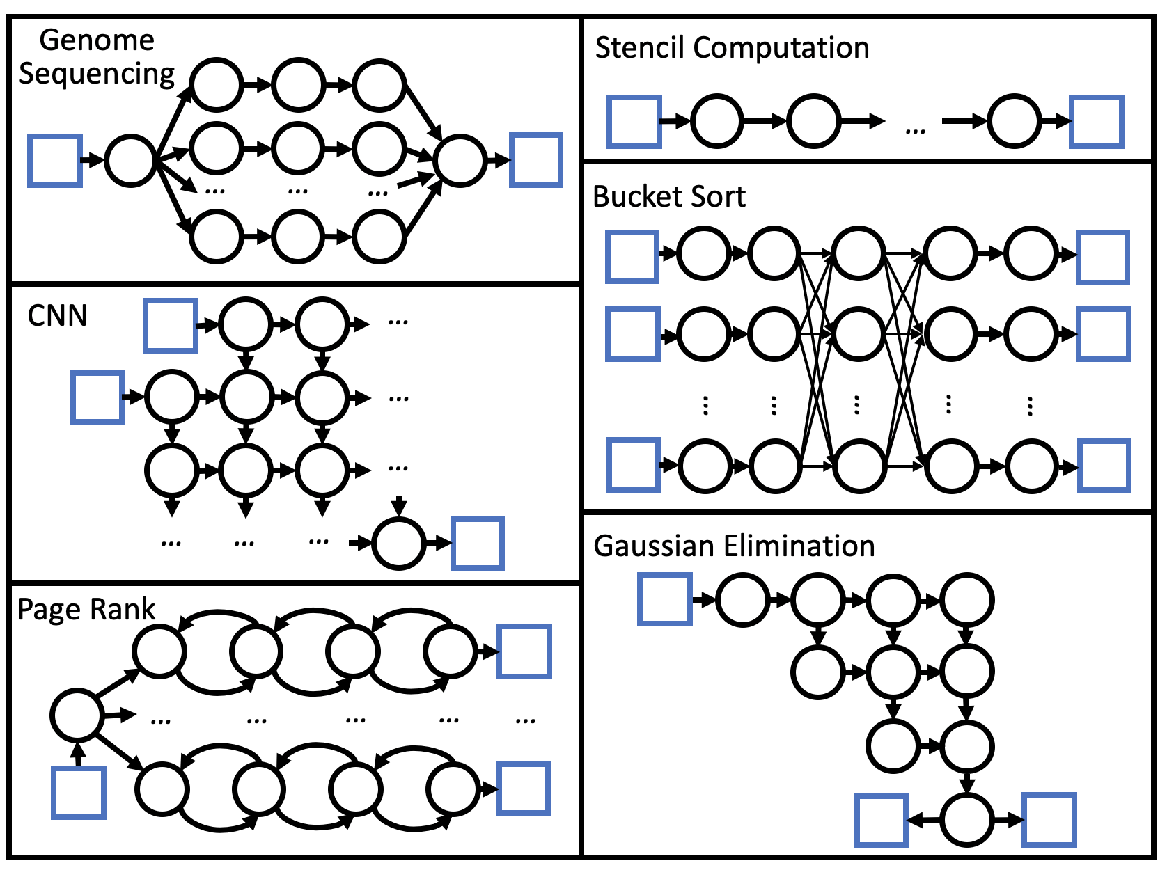
We use two groups of benchmarks to demonstrate the proposed methodologies. We first include six benchmarks that are originally used in AutoBridge (Guo et al., 2021) to showcase the frequency improvement from co-optimization of HLS and physical design. AutoBridge uses six representative benchmark designs with different topologies and changes the parameter of the benchmarks to generate a set of designs with varying sizes on both the U250 and the U280 board. The six designs are all large-scale designs implemented and optimized by HLS experts. Figure 15 shows the topology of the benchmarks. Note that even for those benchmarks that seem regular (e.g., CNN), the location constraints from peripheral IPs can highly distort their physical layouts.
-
•
The stencil designs created by the SODA (Chi et al., 2018b) compiler are a set of kernels in linear topologies.
- •
-
•
The CNN accelerators created by the PolySA (Cong and Wang, 2018) compiler are in a grid topology.
-
•
The HBM graph processing design (Chi et al., 2020) performs the page rank algorithm. It features eight sets of processing units and one central controller. This design also contains dependency cycles, if viewed at the granularity of computing kernels.
-
•
The HBM bucket sort design adapted from (Samardzic et al., 2020) which includes 8 parallel processing lanes and two fully-connected layers.
-
•
The Gaussian elimination designs created by AutoSA (Wang et al., 2021) are in triangle topologies.
In addition, we include three additional benchmarks that use a large number of HBM channels to demonstrate the newly-added HBM-specific optimizations. All of the three additional benchmarks will still fail to route with the original AutoBridge. However, our latest optimizations enable them to route successfully with high frequencies.
-
•
The Scalable and Automatic Stencil Acceleration Framework (SASA) (Tian et al., 2022) accelerators where one version uses 24 channels, and the other one uses 27 channels. Compared to the SODA stencil accelerator used in the original AutoBridge paper, the SASA accelerator also has a much more complicated topology.
-
•
The HBM sparse matrix-matrix multiply (SpMM) accelerator (Song et al., 2022b) that uses 29 HBM channels.
-
•
The Sparse matrix-vector multiply (SpMV) accelerators (Song et al., 2022a) where one version uses 20 HBM channels, and another version uses 28 HBM channels.
7.3. Original Evaluation of AutoBridge
By varying the size of the benchmarks, in total we have tested the implementation of 43 designs with different configurations. Among them, 16 designs failed in routing or placement with the baseline CAD flow, compared AutoBridge which succeeds in routing all of them and achieves an average of 274 MHz. For the other 27 designs, we improve the final frequency from 234 MHz to 311 MHz on average. In general, we find that AutoBridge is effective for designs that use up to about 75% of the available resources. We execute our framework on an Intel Xeon CPU running at 2.2GHz. Both the baseline designs and optimized ones are implemented using Vivado with the highest optimization level. The final design checkpoint files of all experiments are available in our open-sourced repository.
In some experiments, we may find that the optimized versions have even slightly smaller resource consumption. Possible reasons are that we adopt a different FIFO template and disable the hierarchy rebuild step during RTL synthesis. Also, as the optimization leads to very different placement results compared to those of the original version, we expect different optimization strategies will be adopted by the physical design tools. The correctness of the code is verified by cycle-accurate simulation and on-board execution.
Next, we present the detailed results of each benchmark.
SODA Stencil Computation.
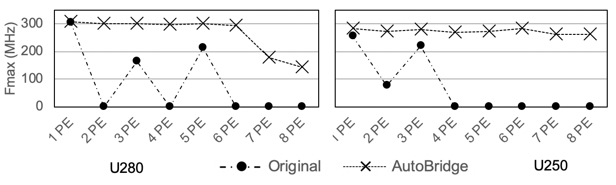
For the stencil computing design, the kernels are connected in a chain format through FIFO channels. By adjusting the number of kernels, we can vary the total size of the design. We test anywhere from one kernel up to eight kernels, and Figure 16 shows final frequency of the eight design configurations on both U250 and U280 FPGAs. In the original flow, many design configurations fail in routing due to routing resource conflicts. Those that are routed successfully still achieve relatively low frequencies. In comparison, with the help of AutoBridge, all design configurations are routed successfully. On average, we improve the timing from 86 MHz to 266 MHz on the U280 FPGA, and from 69 MHz to 273 MHz on the U250 FPGA.
Starting from the seven-kernel design, we observe a frequency decrease on the U280 FPGA. This is because each kernel of the design is very large and uses about half the resources of a slot; thus starting from the seven-kernel design on the relatively small U280, two kernels have to be squeezed into one slot which will cause more severe local routing congestion. Based on this phenomenon, we recommend that users avoid designing very large kernels and instead split the functionality into multiple functions to allow the tool more flexibility in floorplanning the design.
CNN Accelerator.
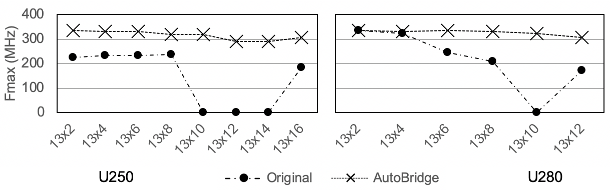
The CNN accelerator consists of identical PEs in a regular grid topology. We adjust the size of the grid from a array up to a array to test the robustness of AutoBridge. Figure 17 shows the result on both U250 and U280 FPGAs.
Although the regular 2-dimensional grid structure is presumed to be FPGA friendly, the actual implementation results from the original tool flow is not satisfying. With the original tool flow, even small-size designs are bounded at around 220 MHz when targeting U250. Designs of larger sizes will fail in placement () or routing ( and ). Although the final frequency is high when the design is small for the original tool flow targeting U280, the timing quality is steadily dropping as the designs become larger.
In contrast, AutoBridge improves from 140 MHz to 316 MHz on U250 on average, and from 214 MHz to 328 MHz on U280. Table 4 lists the resource consumption and cycle counts of the experiments on U250. Statistics on U280 are similar and are omitted here.
| Size | LUT(%) | FF(%) | BRAM(%) | DSP(%) | Cycle | |||||
|---|---|---|---|---|---|---|---|---|---|---|
| orig | opt | orig | opt | orig | opt | orig | opt | orig | opt | |
| 13x2 | 17.82 | 17.90 | 14.11 | 14.25 | 21.69 | 21.67 | 8.57 | 8.57 | 53591 | 53601 |
| 13x4 | 23.52 | 23.59 | 18.98 | 19.04 | 25.74 | 25.73 | 17.03 | 17.03 | 68630 | 68640 |
| 13x6 | 29.26 | 29.24 | 23.86 | 23.80 | 29.80 | 29.78 | 25.50 | 25.50 | 86238 | 86248 |
| 13x8 | 34.98 | 34.90 | 28.72 | 28.56 | 33.85 | 33.84 | 33.96 | 33.96 | 103882 | 103892 |
| 13x10 | 40.71 | 40.48 | 33.58 | 33.25 | 37.91 | 37.89 | 42.42 | 42.42 | 121472 | 121491 |
| 13x12 | - | 46.18 | - | 38.06 | - | 41.95 | - | 50.89 | 139098 | 139108 |
| 13x14 | 52.10 | 51.92 | 43.28 | 42.93 | 46.02 | 46.00 | 59.35 | 59.35 | 156715 | 156725 |
| 13x16 | 57.82 | 57.61 | 48.13 | 47.70 | 50.07 | 50.06 | 67.81 | 67.81 | 174377 | 174396 |
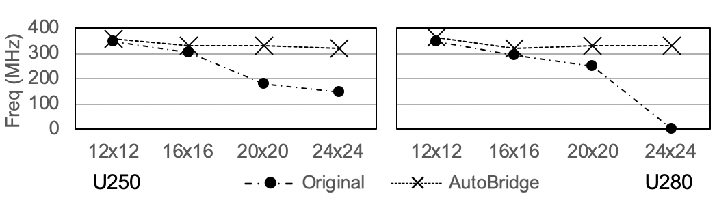
Gaussian elimination.
The PEs in this design form a triangle topology. We adjust the size of the triangle and test on both U250 and U280. Table 5 shows the results. On average, we improve the frequency from 245 MHz to 334 MHz on U250, and from 223 MHz to 335 MHz on U280.
| Size | LUT(%) | FF(%) | BRAM(%) | DSP(%) | Cycle | |||||
|---|---|---|---|---|---|---|---|---|---|---|
| orig | opt | orig | opt | orig | opt | orig | opt | orig | opt | |
| 1212 | 18.58 | 18.69 | 13.05 | 13.14 | 13.24 | 13.21 | 2.79 | 2.79 | 758 | 781 |
| 1616 | 26.62 | 26.68 | 17.36 | 17.30 | 13.24 | 13.21 | 4.99 | 4.99 | 1186 | 1209 |
| 2020 | 38.55 | 38.28 | 23.46 | 23.38 | 13.24 | 13.21 | 7.84 | 7.84 | 1728 | 1738 |
| 2424 | 54.05 | 53.59 | 32.16 | 32.06 | 13.24 | 13.21 | 11.34 | 11.34 | 2361 | 2375 |
HBM Bucket Sort.
The bucket sort design has two complex fully-connected layers. Each fully-connected layer involves an crossbar of FIFO channels, with each FIFO channel being 256-bit wide. AutoBridge pipelines the FIFO channels to alleviate the routing congestion. Table 6 shows the frequency gain, where we improve from 255 MHz to 320 MHz on U280. As the design requires 16 external memory ports and U250 only has 4 available, the test for this design is limited to U280 only.
Because the original source code has enforced a BRAM-based implementation for some small FIFOs, which results in wasted BRAM resources, the results of AutoBridge have slightly lower BRAM and flip-flop consumption than the original implementation. In comparison, we use a different FIFO template that chooses the implementation style (BRAM-based or shift-register-based) based on the area of the FIFO. Cycle accurate simulation has proven the correct functionality of our optimized implementation.
| Fmax (MHz) | LUT % | FF % | BRAM % | DSP % | Cycle | |
|---|---|---|---|---|---|---|
| Original | 255 | 28.44 | 19.11 | 16.47 | 0.04 | 78629 |
| Optimized | 320 | 29.39 | 16.66 | 13.69 | 0.04 | 78632 |
HBM Page Rank.
This design incorporates eight sets of processing units, each interfacing with two HBM ports. There are also centralized control units that exchange control information with five HBM ports. Table 7 shows the experiment results and we improve the final frequency from 136 MHz to 210 MHz on U280.
| Fmax (MHz) | LUT % | FF % | BRAM % | DSP % | Cycle | |
|---|---|---|---|---|---|---|
| Original | 136 | 38.56 | 26.97 | 26.74 | 14.43 | 120458 |
| Optimized | 210 | 39.49 | 27.53 | 30.08 | 14.43 | 120495 |
7.4. HBM-Specific Optimizations
In this section, we use four real-world designs from premium academic conferences or journals to demonstrate the effects of our HBM-specific optimizations. We select those designs as they use a large number of HBM channels, which brings about a serious timing closure challenge.
HBM SpMM and SpMV Accelerators.
The sparse matrix-matrix multiplication (SpMM) and the sparse matrix-vector multiplication (SpMV) accelerators leverage the async_mmap API, automatic HBM channel binding, die-crossing wire adjusting, and multi-floorplan generation to achieve the best performance. We implement two versions of the SpMV accelerator, SpMV_A24 and SpMV_A16, with different numbers of parallel processing elements. We report the user clock and HBM clock frequencies and the resource utilization in Table 8. We have improved both the user clock and the HBM clock frequencies for the three designs. Especially for SpMV_A24, we have improved the user clock frequency from 193 MHz to 283 MHz and the HBM clock frequency from 430 MHz to 450 MHz. With the async_mmap, we significantly reduced BRAM utilization – for SpMM and SpMV_A24, we reduced 10% of the total BRAM utilization.
| Fuser/Fhbm (MHz) | LUT % | FF % | BRAM % | URAM % | DSP % | |
|---|---|---|---|---|---|---|
| Orig, SpMM | 216/424 | 37.35 | 31.34 | 71.55 | 53.33 | 40.97 |
| Opt, SpMM | 245/427 | 39.40 | 28.47 | 60.91 | 53.33 | 40.97 |
| Orig, SpMV_A16 | 233/450 | 21.70 | 17.36 | 42.63 | 40.00 | 8.89 |
| Opt, SpMV_A16 | 299/450 | 22.75 | 15.06 | 35.52 | 40.00 | 8.89 |
| Orig, SpMV_A24 | 193/430 | 27.95 | 22.46 | 58.31 | 40.00 | 14.92 |
| Opt, SpMV_A24 | 283/450 | 29.76 | 19.11 | 48.21 | 40.00 | 14.92 |
HBM Stencil Accelerators by SASA.
The SASA design incorporates the async_mmap API, automatic HBM channel binding, die-crossing wire adjusting, and floorplan candidate generation to push the user clock frequency above 225 MHz and the HBM clock frequency to 450 MHz, which enables the accelerator to fully utilize the HBM bandwidth. For stencil algorithms that have a low number of iterations, SASA will leverage efficient spatial parallelism where each kernel read one tile of input data and additional halo data from neighboring tiles at the start. Then each kernel performs the computation for all iterations (if any) without synchronization. Each kernel works in a streaming pattern and uses at least two HBM banks to store the input and output. The original design based on mmap fails to meet the frequency requirement. With the async_mmap API, we are able to significantly reduce the BRAM utilization. With all optimizations, the two selected designs achieve 241 MHz and 250 MHz respectively.
| Fuser/Fhbm (MHz) | LUT % | FF % | BRAM % | URAM % | DSP % | |
|---|---|---|---|---|---|---|
| Orig, SASA-1 | 169/295 | 32.2 | 21.98 | 18.45 | 0 | 17.02 |
| Opt, SASA-1 | 241/450 | 36.04 | 18.09 | 0 | 0 | 17.02 |
| Orig, SASA-2 | Failed/Failed | 35.9 | 30.94 | 23.88 | 0 | 47.87 |
| Opt, SASA-2 | 250/450 | 40.63 | 27.57 | 6.7 | 0 | 47.87 |
Results of Multi-Floorplan Generation
For HBM designs that are sensitive to logic resource utilization and routing resource utilization at the same time, we generate a set of Pareto-optimal floorplanning and implement all of them to explore the potentially best results. Table 10 shows the corresponding achievable frequency. The number of generated floorplan candidates is related to the granularity of the design. Designs with larger tasks have less flexibility in floorplanning, thus there are fewer points on the Pareto-optimal curve. It remains as future work to automatically split large tasks and fuse small tasks to better facilitate the floorplan process.
As can be seen, even with the same set of optimization techniques, slightly different floorplanning may lead to non-trivial variation in the final achievable frequency. At this stage, we treat the downstream tools as a black box, so we implement all generated floorplan schemes in parallel to search for the best results. How to better predict the final frequency and skip unpromising floorplans in an early stage remains as future work.
| Design | Baseline | Multi-Floorplan Generation | Max | Min |
|---|---|---|---|---|
| SASA | 169 MHz | 230 / 236 / 241 / Failed / Failed / 168 MHz | 241 MHz | Failed |
| SpMM | 216 MHz | 242 / 232 / 231 / 238 / 194 / 215 / 245 MHz | 245 MHz | 194 MHz |
| SpMV-24 | 194 MHz | 253 / 257 / 276 / 173 / 270 / 259 / 251 / 244 / 261 / 280 / 284 MHz | 284 MHz | 173 MHz |
| SpMV-16 | 233 MHz | 300 / 285 MHz | 300 MHz | 285 MHz |
7.5. Control Experiments
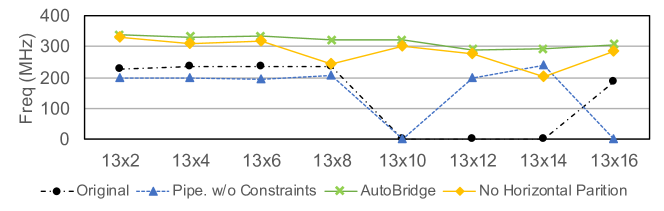
First, we test whether the frequency gain comes from the combination of pipelining and HLS-floorplanning, or simply pipelining alone. To do this, we set a control group where we perform floorplanning and pipelining as usual, but we do not pass the floorplan constraints to the physical design tools. The blue curve with triangle markers in Figure 19 shows the results. As can be seen, the control group has a lower frequency than the original design for small sizes and has limited improvements over the original designs for large sizes. In all experiments, the group with both pipelining and floorplan constraints (green curve with crossing markers) has the highest frequency. This experiment proves that the frequency gain is not simply a result of more pipelining.
Meanwhile, if we only do floorplanning without pipelining, obviously the frequency will be much degraded, as visualized by Fig. 3.
Second, we test the effectiveness of setting a slot boundary based on the DDR controllers. We run a set of experiments where we only divide the FPGA into four slots based on the die boundaries, minus the division in the middle column. The yellow curve with diamond markers in Figure 19 shows the results. As can be seen, it achieves lower frequency compared to our default eight-slot scheme.
7.6. Scalability
To show that the tool works well on designs with large numbers of small functions, we utilize the CNN experiments to test the scalability of our algorithms, as the CNN designs have the most vertices (HLS functions) and edges. Table 11 lists The compile time overhead for the floorplanning and the latency balancing when using Gurobi as the ILP solver444Meanwhile, we observed that many open-source ILP solvers are much slower.. For the largest CNN accelerator that has 493 modules and 925 FIFO connections, the floorplan step only takes around 20 seconds and the latency balancing step takes 0.03s. Usually, FPGA designs are not likely to have this many modules and connections (Xilinx-Vitis-Library, 2020) (Intel-OpenCL-Examples, 2020), and our method is fast enough.
| Size | # V | # E | Div-1 | Div-2 | Div-3 | Re-balance |
|---|---|---|---|---|---|---|
| 13 2 | 87 | 141 | 0.02 s | 0.02 s | 0.01 s | 0.01 s |
| 13 4 | 145 | 253 | 0.05 s | 0.02 s | 0.20 s | 0.01 s |
| 13 6 | 203 | 365 | 0.07 s | 1.02 s | 0.56 s | 0.01 s |
| 13 8 | 261 | 477 | 0.07 s | 1.07 s | 3.58 s | 0.01 s |
| 13 10 | 319 | 589 | 3.17 s | 1.61 s | 2.63 s | 0.01 s |
| 13 12 | 377 | 701 | 3.42 s | 1.43 s | 9.84 s | 0.01 s |
| 13 14 | 435 | 813 | 3.54 s | 1.55 s | 6.18 s | 0.03 s |
| 13 16 | 493 | 925 | 4.95 s | 2.02 s | 12.56 s | 0.03 s |
8. Related Work
Layout-Aware HLS Optimization. Previous works have studied how to couple the physical design process with HLS in a fine-grained manner. Zheng et al. (Zheng et al., 2014) propose to iteratively run placement and routing for fine-grained calibration of the delay estimation of wires. The long run time of placement and routing prohibits their methods from benefiting large-scale designs, and their experiments are all based on small examples (1000s of registers and 10s of DSPs in their experiments). Cong et. al. (Cong et al., 2004) presented placement-driven scheduling and binding for multi-cycle communications in an island-style reconfigurable architecture. Xu et. al. (Xu and Kurdahi, 1997) proposed to predict a register-level floorplan to facilitate the binding process. Some commercial HLS tools (Cadence, 2020; Synopsys, 2020) have utilized the results of logic synthesis to calibrate HLS delay estimation, but they do not consider the interconnect delays.
The previous approaches share the common aspect of focusing on the fine-grained interaction between physical design and upstream synthesis, where individual operators and the associated wires and registers are all involved during the delay prediction and iterative pipeline co-optimization. While such a fine-grained method can be effective on relatively small designs and FPGA devices, it is too expensive (if not infeasible) for today’s large designs targeting multi-die FPGAs, where each implementation iteration may take days to complete.
In contrast, we focus on a coarse-grained approach that only pipelines the channels that span long distances and guides the detailed placement.
Other works have studied methods to predict delay estimation at the behavior level. Guo et al. (Guo et al., 2020) proposed to calibrate the estimated delay for operators with large broadcast factors by pre-characterizing benchmarks with different broadcast factors. Tan et al. (Tan et al., 2015) showed that the delay prediction of logic operations (e.g., AND, OR, NOT, etc) by HLS tools is too conservative. Therefore they consider the technology mapping for logic operations. These works mainly target local operators and have limited effects on global interconnects. Zhao et al. (Zhao et al., 2019) used machine learning to predict how manual pragmas affect routing congestion.
In addition, Cong et al. (Cong et al., 2018b) presented tools to allow users to insert additional buffers to the designated datapath. Chen et al. (Chen et al., 2019) proposed to add additional registers to the pipelined datapath during HLS synthesis based on the profiling results on the CHStone benchmark. (Zhang et al., 2019) proposes to generate floorplanning constraints only for systolic array designs, and their method does not consider the interaction with peripheral IPs such as DDR controllers. In comparison, our work is fully-automated for general designs and our register insertion is accurate due to HLS-floorplan co-design.
Optimization for Multi-Die FPGAs. To adapt to multi-die FPGAs, previous works have studied how to partition the entire design or memories among different dies (Roy and Sechen, 1993; Cherabuddi and Bayoumi, 1994; Mao et al., 2016; Hahn Pereira and Betz, 2014; Nasiri et al., 2015; Karypis et al., 1999; Voss et al., 2019). These methods are all based on RTL inputs, thus the partition method must observe the cycle-accurate specification. (Hahn Pereira and Betz, 2014; Nasiri et al., 2015) try to modify the cost function of placement to reduce die-crossing. This will lead to designs confined in fewer dies with a higher level of local congestion. Zha et al. (Zha and Li, 2020) propose methods to virtualize the FPGA and let different applications execute at different partitions. Xiao et al. (Xiao et al., 2020; Xiao et al., 2022) propose methods to split the placement and routing of different parts of the design through dynamic reconfiguration.
Floorplanning Algorithms. Floorplanning has been extensively studied (Alpert et al., 2008; Cheng and Wong, 2006; Banerjee et al., 2009; Murray and Betz, 2015). Conventionally, floorplanning consists of 1) feasible topology generation and 2) determining the aspect ratios for goals such as minimal total wire length. In the existing FPGA CAD flows, the floorplanning step works on RTL input. In contrast, we propose to perform coarse-grained floorplanning during the HLS step to help gain layout information for the HLS tool. Similar to (Lauther, 1988; La Potin and Director, 1986; Modarres and Kelapure, 1987), our algorithm adopts the idea of the partitioning-based approach. As our problem size is relatively small, we use ILP for each partitioning.
Throughput Analysis of Dataflow Designs. Various dataflow models have been proposed in other literature, such as the Kahn Process Network (KPN) (Gilles, 1974), Synchronous Data Flow (SDF) (Lee and Messerschmitt, 1987b), among many others. The more simplified the model is, the more accurately we can analyze its throughput. In the SDF model, it is restricted that the number of data produced or consumed by a process for each firing is fixed and known. Therefore, it is possible to analytically compute the influence of additional latency on throughput (Ghamarian et al., 2006). The latency insensitive theory (LIT) (Carloni and Sangiovanni-Vincentelli, 2000; Lu and Koh, 2003, 2006; Collins and Carloni, 2007; Abbas and Betz, 2018) also enforces similar restrictions as SDF. (Venkataramani and Gu, 2014) proposes methods to insert delays when composing IP blocks of different latency. (Josipović et al., 2020) studies the buffer placement problem in dataflow circuits (Josipović et al., 2018; Cheng et al., 2020; Cheng et al., 2022; Cheng et al., 2021). Other works have studied how to map dataflow programs to domain-specific coarse-grained reconfigurable architectures (Weng et al., 2020a; Weng et al., 2020b; Dadu et al., 2019, 2021).
In our scenario, each function will be compiled into an FSM that can be arbitrarily complex, thus it is difficult to quantitatively analyze the effect of the added latency on the total execution cycles. We adopt a conservative approach to balance the added latency on all reconvergent paths.
9. Future Work
While TAPA has already improved significantly on the expressiveness and timing closure, there is a myriad of opportunities to further advance the tool. We list several challenges that we aim to address in the future.
-
•
Reduce the compile time by integrating RapidStream (Guo et al., 2022). RapidStream builds on top of the idea of HLS-floorplanning co-optimization, and it further splits the design for parallel placement and routing. When tested on the Xilinx U250 FPGA with a set of realistic HLS designs, RapidStream achieves a 5-7 reduction in compile time and up to 1.3 increase in frequency when compared to a commercial-off-the-shelf toolchain. We are in the progress to integrate RapidStream with TAPA.
-
•
Support more flexible inter-task communication patterns. Currently, TAPA tasks can only communicate with each other through streams. We are extending the infrastructure to support buffer-based channels between tasks for richer expressiveness.
-
•
Task-level compiler optimization. As of now, TAPA delegates the compilation of each task to existing HLS tools and does not perform inter-task optimizations. This limitation requires that users come up with a good partitioning of the application into tasks of suitable sizes. We aim to add additional task-level optimization such as task splitting, task fusion, task hierarchy rebuild, etc. to further co-optimize the task hierarchy and the floorplanning process.
-
•
Support designs with a hybrid of RTL and HLS tasks. The floorplan-guided pipeline methodology could apply to RTL tasks as long as they adhere to pre-defined latency-insensitive interfaces. Although we have explored applying the technique to RTL projects (Qiao et al., 2021, 2022), more efforts are needed to provide an automated solution.
10. Conclusions
In this paper, we present the TAPA framework, an efficient task-parallel programming tool for modern FPGAs. TAPA includes a set of convenient APIs to increase design efficiency. In addition, we tackle the challenge of high-frequency HLS design on multi-die FPGAs by coupling floorplanning and pipelining to effectively insert registers on the long cross-die interconnects. We present a set of optimizations specifically tailored for HBM devices, including automatic HBM port binding, floorplan solution space exploration, and a customized programming API to minimize the area overhead of HBM IO modules. Our framework, TAPA, interfaces with the commercial FPGA design tool flow. It improves the average frequency of 43 designs from 147 MHz to 297 MHz with a negligible area overhead. TAPA has been used in multiple projects to improve the design efficiency and final frequency (Chi et al., 2022; Wang et al., 2021; Song et al., 2022a; Song et al., 2022b; Chi and Cong, 2020).
Acknowledgements.
We greatly thank Wuxi Li, Jianyi Cheng, Luciano Lavagno, Gai Liu, Zixuan Jiang, Yifan Yuan and the anonymous reviewers for their valuable feedback. This work is partially supported by the CRISP Program, members from the CDSC Industrial Partnership Program, the Intel/NSF CAPA program, the NSF NeuroNex Award No. DBI-1707408, the NIH Award No. U01MH117079, the NSERC Discovery Grant RGPIN-2019-04613 and DGECR-2019-00120, and the CFI John R. Evans Leaders Fund. The authors acknowledge the valuable support of the Xilinx Adaptive Compute Clusters (XACC) Program. We thank Gurobi and GNU Parallel for their support to academia.References
- (1)
- Abbas and Betz (2018) Mustafa Abbas and Vaughn Betz. 2018. Latency insensitive design styles for FPGAs. In 2018 28th International Conference on Field Programmable Logic and Applications (FPL). IEEE, 360–3607.
- Alpert et al. (2008) Charles J Alpert, Dinesh P Mehta, and Sachin S Sapatnekar. 2008. Handbook of algorithms for physical design automation. CRC press.
- Banerjee et al. (2009) Pritha Banerjee, Susmita Sur-Kolay, and Arijit Bishnu. 2009. Fast unified floorplan topology generation and sizing on heterogeneous FPGAs. IEEE Transactions on Computer-Aided Design of Integrated Circuits and Systems 28, 5 (2009), 651–661.
- Breuer (1977) Melvin A Breuer. 1977. A class of min-cut placement algorithms. In Proceedings of the 14th Design Automation Conference. 284–290.
- Buck (1993) Joseph T. Buck. 1993. Scheduling Dynamic Dataflow Graphs with Bounded Memory Using the Token Flow Model. Ph.D. Dissertation.
- Cadence (2020) Cadence. 2020. https://www.cadence.com/
- Carloni et al. (2001) Luca P Carloni, Kenneth L McMillan, and Alberto L Sangiovanni-Vincentelli. 2001. Theory of latency-insensitive design. IEEE Transactions on computer-aided design of integrated circuits and systems 20, 9 (2001), 1059–1076.
- Carloni and Sangiovanni-Vincentelli (2000) Luca P Carloni and Alberto L Sangiovanni-Vincentelli. 2000. Performance analysis and optimization of latency insensitive systems. In Proceedings of the 37th Annual Design Automation Conference. 361–367.
- Chen et al. (2019) Yu Ting Chen, Jin Hee Kim, Kexin Li, Graham Hoyes, and Jason H Anderson. 2019. High-Level Synthesis Techniques to Generate Deeply Pipelined Circuits for FPGAs with Registered Routing. In 2019 International Conference on Field-Programmable Technology (ICFPT). IEEE, 375–378.
- Cheng et al. (2020) Jianyi Cheng, Lana Josipovic, George A Constantinides, Paolo Ienne, and John Wickerson. 2020. Combining Dynamic & Static Scheduling in High-level Synthesis. In The 2020 ACM/SIGDA International Symposium on Field-Programmable Gate Arrays. 288–298.
- Cheng et al. (2021) Jianyi Cheng, Lana Josipović, George A Constantinides, Paolo Ienne, and John Wickerson. 2021. DASS: Combining Dynamic & Static Scheduling in High-Level Synthesis. IEEE Transactions on Computer-Aided Design of Integrated Circuits and Systems 41, 3 (2021), 628–641.
- Cheng et al. (2022) Jianyi Cheng, John Wickerson, and George A Constantinides. 2022. Finding and finessing static islands in dynamically scheduled circuits. In Proceedings of the 2022 ACM/SIGDA International Symposium on Field-Programmable Gate Arrays. 89–100.
- Cheng and Wong (2006) Lei Cheng and Martin DF Wong. 2006. Floorplan design for multimillion gate FPGAs. IEEE Transactions on Computer-Aided Design of Integrated Circuits and Systems 25, 12 (2006), 2795–2805.
- Cherabuddi and Bayoumi (1994) Raghava V Cherabuddi and Magdy A Bayoumi. 1994. Automated system partitioning for synthesis of multi-chip modules. In Proceedings of 4th Great Lakes Symposium on VLSI. IEEE, 15–20.
- Chi and Cong (2020) Yuze Chi and Jason Cong. 2020. Exploiting Computation Reuse for Stencil Accelerators. In DAC.
- Chi et al. (2018a) Yuze Chi, Jason Cong, Peng Wei, and Peipei Zhou. 2018a. SODA : Stencil with Optimized Dataflow Architecture. In ICCAD.
- Chi et al. (2018b) Yuze Chi, Jason Cong, Peng Wei, and Peipei Zhou. 2018b. SODA: stencil with optimized dataflow architecture. In 2018 IEEE/ACM International Conference on Computer-Aided Design (ICCAD). IEEE, 1–8.
- Chi et al. (2020) Yuze Chi, Licheng Guo, Young-kyu Choi, Jie Wang, and Jason Cong. 2020. Extending High-Level Synthesis for Task-Parallel Programs. arXiv preprint arXiv:2009.11389 (2020).
- Chi et al. (2022) Yuze Chi, Licheng Guo, and Jason Cong. 2022. Accelerating SSSP for Power-Law Graphs. In Proceedings of the 2022 ACM/SIGDA International Symposium on Field-Programmable Gate Arrays. 190–200.
- Choi et al. (2021) Young-kyu Choi, Yuze Chi, Weikang Qiao, Nikola Samardzic, and Jason Cong. 2021. HBM Connect: High-Performance HLS Interconnect for FPGA HBM. In Proceedings of the 2021 ACM/SIGDA International Symposium on Field-Programmable Gate Arrays.
- Choi et al. (2020) Young-kyu Choi, Yuze Chi, Jie Wang, Licheng Guo, and Jason Cong. 2020. When HLS Meets FPGA HBM: Benchmarking and Bandwidth Optimization. arXiv preprint arXiv:2010.06075 (2020).
- Collins and Carloni (2007) Rebecca L Collins and Luca P Carloni. 2007. Topology-based optimization of maximal sustainable throughput in a latency-insensitive system. In Proceedings of the 44th annual Design Automation Conference. 410–415.
- Cong et al. (2004) Jason Cong, Yiping Fan, Guoling Han, Xun Yang, and Zhiru Zhang. 2004. Architecture and synthesis for on-chip multicycle communication. IEEE Transactions on Computer-Aided Design of Integrated Circuits and Systems 23, 4 (2004), 550–564.
- Cong and Wang (2018) Jason Cong and Jie Wang. 2018. PolySA: polyhedral-based systolic array auto-compilation. In 2018 IEEE/ACM International Conference on Computer-Aided Design (ICCAD). IEEE, 1–8.
- Cong et al. (2018a) Jason Cong, Peng Wei, Cody Hao Yu, and Peipei Zhou. 2018a. Latte: Locality Aware Transformation for High-Level Synthesis. In FCCM.
- Cong et al. (2018b) Jason Cong, Peng Wei, Cody Hao Yu, and Peipei Zhou. 2018b. Latte: Locality aware transformation for high-level synthesis. In 2018 IEEE 26th Annual International Symposium on Field-Programmable Custom Computing Machines. IEEE, 125–128.
- Cong and Zhang (2006) Jason Cong and Zhiru Zhang. 2006. An efficient and versatile scheduling algorithm based on SDC formulation. In 2006 43rd ACM/IEEE Design Automation Conference. IEEE, 433–438.
- Dadu et al. (2021) Vidushi Dadu, Sihao Liu, and Tony Nowatzki. 2021. Polygraph: Exposing the value of flexibility for graph processing accelerators. In 2021 ACM/IEEE 48th Annual International Symposium on Computer Architecture (ISCA). IEEE, 595–608.
- Dadu et al. (2019) Vidushi Dadu, Jian Weng, Sihao Liu, and Tony Nowatzki. 2019. Towards general purpose acceleration by exploiting common data-dependence forms. In Proceedings of the 52nd Annual IEEE/ACM International Symposium on Microarchitecture. 924–939.
- Dagum and Menon (1998) Leonardo Dagum and Ramesh Menon. 1998. OpenMP: An Industry Standard API for Shared-Memory Programming. IEEE Computational Science and Engineering 5, 1 (1998).
- Dai et al. (2016) Guohao Dai, Yuze Chi, Yu Wang, and Huazhong Yang. 2016. FPGP: Graph Processing Framework on FPGA A Case Study of Breadth-First Search. In FPGA.
- Dai et al. (2017) Guohao Dai, Tianhao Huang, Yuze Chi, Ningyi Xu, Yu Wang, and Huazhong Yang. 2017. ForeGraph: Exploring Large-scale Graph Processing on Multi-FPGA Architecture. In FPGA.
- Dunlop et al. (1985) Alfred E Dunlop, Brian W Kernighan, et al. 1985. A procedure for placement of standard cell VLSI circuits. IEEE Transactions on Computer-Aided Design 4, 1 (1985), 92–98.
- Ghamarian et al. (2006) Amir Hossein Ghamarian, Marc CW Geilen, Sander Stuijk, Twan Basten, Bart D Theelen, Mohammad Reza Mousavi, Arno JM Moonen, and Marco JG Bekooij. 2006. Throughput analysis of synchronous data flow graphs. In Sixth International Conference on Application of Concurrency to System Design (ACSD’06). IEEE, 25–36.
- Gilles (1974) KAHN Gilles. 1974. The semantics of a simple language for parallel programming. Information processing 74 (1974), 471–475.
- Guo et al. (2021) Licheng Guo, Yuze Chi, Jie Wang, Jason Lau, Weikang Qiao, Ecenur Ustun, Zhiru Zhang, and Jason Cong. 2021. AutoBridge: Coupling Coarse-Grained Floorplanning and Pipelining for High-Frequency HLS Design on Multi-Die FPGAs. In FPGA.
- Guo et al. (2020) Licheng Guo, Jason Lau, Yuze Chi, Jie Wang, Cody Hao Yu, Zhe Chen, Zhiru Zhang, and Jason Cong. 2020. Analysis and Optimization of the Implicit Broadcasts in FPGA HLS to Improve Maximum Frequency. In 57th ACM/IEEE Design Automation Conference. https://doi.org/10.1109/DAC18072.2020.9218718
- Guo et al. (2019) Licheng Guo, Jason Lau, Zhenyuan Ruan, Peng Wei, and Jason Cong. 2019. Hardware acceleration of long read pairwise overlapping in genome sequencing: A race between FPGA and GPU. In 2019 IEEE 27th Annual International Symposium on Field-Programmable Custom Computing Machines (FCCM). IEEE, 127–135.
- Guo et al. (2022) Licheng Guo, Pongstorn Maidee, Yun Zhou, Chris Lavin, Jie Wang, Yuze Chi, Weikang Qiao, Alireza Kaviani, Zhiru Zhang, and Jason Cong. 2022. RapidStream: Parallel Physical Implementation of FPGA HLS Designs. In Proceedings of the 2022 ACM/SIGDA International Symposium on Field-Programmable Gate Arrays. 1–12.
- Gurobi (2020) Gurobi. 2020. https://www.gurobi.com/
- Hahn Pereira and Betz (2014) Andre Hahn Pereira and Vaughn Betz. 2014. Cad and routing architecture for interposer-based multi-FPGA systems. In Proceedings of the 2014 ACM/SIGDA international symposium on Field-programmable gate arrays. 75–84.
- Hoare (1978) C. A. R. Hoare. 1978. Communicating Sequential Processes. Commun. ACM 21, 8 (1978).
- Intel (2020) Intel. 2020. Intel Stratix 10 FPGA. https://www.intel.com/content/dam/www/programmable/us/en/pdfs/literature/hb/stratix-10/s10-overview.pdf
- Intel-OpenCL-Examples (2020) Intel-OpenCL-Examples. 2020. https://www.intel.com/content/www/us/en/programmable/products/design-software/embedded-software-developers/opencl/support.html
- Josipović et al. (2018) Lana Josipović, Radhika Ghosal, and Paolo Ienne. 2018. Dynamically scheduled high-level synthesis. In Proceedings of the 2018 ACM/SIGDA International Symposium on Field-Programmable Gate Arrays. 127–136.
- Josipović et al. (2020) Lana Josipović, Shabnam Sheikhha, Andrea Guerrieri, Paolo Ienne, and Jordi Cortadella. 2020. Buffer placement and sizing for high-performance dataflow circuits. In The 2020 ACM/SIGDA International Symposium on Field-Programmable Gate Arrays. 186–196.
- Kahn (1974) Gilles Kahn. 1974. The Semantics of a Simple Language for Parallel Programming. In IFIP.
- Karypis et al. (1999) George Karypis, Rajat Aggarwal, Vipin Kumar, and Shashi Shekhar. 1999. Multilevel hypergraph partitioning: applications in VLSI domain. IEEE Transactions on Very Large Scale Integration (VLSI) Systems 7, 1 (1999), 69–79.
- La Potin and Director (1986) David P La Potin and Stephen W Director. 1986. Mason: A global floorplanning approach for VLSI design. IEEE transactions on computer-aided design of integrated circuits and systems 5, 4 (1986), 477–489.
- Lauther (1988) Ulrich Lauther. 1988. A min-cut placement algorithm for general cell assemblies based on a graph representation. In Papers on Twenty-five years of electronic design automation. 182–191.
- Lee and Messerschmitt (1987a) Edward A. Lee and David G. Messerschmitt. 1987a. Synchronous Data Flow. IEEE 75, 9 (1987).
- Lee and Messerschmitt (1987b) Edward A Lee and David G Messerschmitt. 1987b. Synchronous data flow. Proc. IEEE 75, 9 (1987), 1235–1245.
- Leiserson and Saxe (1991) Charles E Leiserson and James B Saxe. 1991. Retiming synchronous circuitry. Algorithmica 6, 1-6 (1991), 5–35.
- Li (2018) Heng Li. 2018. Minimap2: pairwise alignment for nucleotide sequences. Bioinformatics 34, 18 (2018), 3094–3100.
- Li et al. (2020) Jiajie Li, Yuze Chi, and Jason Cong. 2020. HeteroHalide: From Image Processing DSL to Efficient FPGA Acceleration. In FPGA.
- Lu and Koh (2003) Ruibing Lu and Cheng-Kok Koh. 2003. Performance optimization of latency insensitive systems through buffer queue sizing of communication channels. In ICCAD-2003. International Conference on Computer Aided Design (IEEE Cat. No. 03CH37486). IEEE, 227–231.
- Lu and Koh (2006) Ruibing Lu and Cheng-Kok Koh. 2006. Performance analysis of latency-insensitive systems. IEEE Transactions on Computer-Aided Design of Integrated Circuits and Systems 25, 3 (2006), 469–483.
- Maidee et al. (2003) Pongstorn Maidee, Cristinel Ababei, and Kia Bazargan. 2003. Fast timing-driven partitioning-based placement for island style FPGAs. In Proceedings of the 40th annual design automation conference. 598–603.
- Mao et al. (2016) Fubing Mao, Wei Zhang, Bo Feng, Bingsheng He, and Yuchun Ma. 2016. Modular placement for interposer based multi-FPGA systems. In 2016 International Great Lakes Symposium on VLSI (GLSVLSI). IEEE, 93–98.
- Minimum-Cut (2020) Minimum-Cut. 2020. https://en.wikipedia.org/wiki/Minimum_cut
- Modarres and Kelapure (1987) H Modarres and A Kelapure. 1987. AN AUTOMATIC FLOORPLANNER FOR UP TO 100,000 GATES. VLSI Systems Design 8, 13 (1987), 38.
- Murray and Betz (2015) Kevin E Murray and Vaughn Betz. 2015. HETRIS: Adaptive floorplanning for heterogeneous FPGAs. In 2015 International Conference on Field Programmable Technology (FPT). IEEE, 88–95.
- Nasiri et al. (2015) Ehsan Nasiri, Javeed Shaikh, Andre Hahn Pereira, and Vaughn Betz. 2015. Multiple dice working as one: CAD flows and routing architectures for silicon interposer FPGAs. IEEE Transactions on Very Large Scale Integration Systems 24, 5 (2015), 1821–1834.
- Papaphilippou et al. (2020) Philippos Papaphilippou, Jiuxi Meng, and Wayne Luk. 2020. High-Performance FPGA Network Switch Architecture. In FPGA.
- Parhi (2007) Keshab K Parhi. 2007. VLSI digital signal processing systems: design and implementation. John Wiley & Sons.
- Peng and Puroshothaman (1991) Wuxu Peng and S Puroshothaman. 1991. Data flow analysis of communicating finite state machines. ACM Transactions on Programming Languages and Systems (TOPLAS) 13, 3 (1991), 399–442.
- Peterson (1977) James L Peterson. 1977. Petri Nets. Comput. Surveys 9, 3 (1977).
- Pu et al. (2017) Jing Pu, Steven Bell, Xuan Yang, Jeff Setter, Stephen Richardson, Jonathan Ragan-Kelley, and Mark Horowitz. 2017. Programming Heterogeneous Systems from an Image Processing DSL. TACO 14, 3 (2017).
- Qiao et al. (2022) Weikang Qiao, Licheng Guo, Zhenman Fang, Mau-Chung Frank Chang, and Jason Cong. 2022. TopSort: A High-Performance Two-Phase Sorting Accelerator Optimized on HBM-based FPGAs. In 2022 IEEE 30th Annual International Symposium on Field-Programmable Custom Computing Machines (FCCM). IEEE, 1–1.
- Qiao et al. (2021) Weikang Qiao, Jihun Oh, Licheng Guo, Mau-Chung Frank Chang, and Jason Cong. 2021. FANS: FPGA-Accelerated Near-Storage Sorting. In 2021 IEEE 29th Annual International Symposium on Field-Programmable Custom Computing Machines (FCCM). IEEE, 106–114.
- Roy and Sechen (1993) Kalapi Roy and Carl Sechen. 1993. A timing driven N-way chip and multi-chip partitioner. In Proceedings of 1993 International Conference on Computer Aided Design (ICCAD). IEEE, 240–247.
- Samardzic et al. (2020) Nikola Samardzic, Weikang Qiao, Vaibhav Aggarwal, Mau-Chung Frank Chang, and Jason Cong. 2020. Bonsai: High-Performance Adaptive Merge Tree Sorting. In 2020 ACM/IEEE 47th Annual International Symposium on Computer Architecture. IEEE, 282–294.
- Santos and Toffolo (2020) H.G. Santos and T.A.M. Toffolo. 2020. Python MIP (Mixed-Integer Linear Programming) Tools. https://pypi.org/project/mip/
- Sohrabizadeh et al. (2022) Atefeh Sohrabizadeh, Yuze Chi, and Jason Cong. 2022. StreamGCN: Accelerating Graph Convolutional Networks with Streaming Processing. In 2022 IEEE Custom Integrated Circuits Conference (CICC). IEEE, 1–8.
- Sohrabizadeh et al. (2020) Atefeh Sohrabizadeh, Jie Wang, and Jason Cong. 2020. End-to-end optimization of deep learning applications. In Proceedings of the 2020 ACM/SIGDA International Symposium on Field-Programmable Gate Arrays. 133–139.
- Song et al. (2022a) Linghao Song, Yuze Chi, Licheng Guo, and Jason Cong. 2022a. Serpens: A High Bandwidth Memory Based Accelerator for General-Purpose Sparse Matrix-Vector Multiplication. In 2022 59th ACM/IEEE Design Automation Conference (DAC).
- Song et al. (2022b) Linghao Song, Yuze Chi, Atefeh Sohrabizadeh, Young kyu Choi, Jason Lau, and Jason Cong. 2022b. Sextans: A Streaming Accelerator for General-Purpose Sparse-Matrix Dense-Matrix Multiplication. In The 2022 ACM/SIGDA International Symposium on Field-Programmable Gate Arrays.
- Synopsys (2020) Synopsys. 2020. https://www.synopsys.com/
- Tan et al. (2015) Mingxing Tan, Steve Dai, Udit Gupta, and Zhiru Zhang. 2015. Mapping-aware constrained scheduling for LUT-based FPGAs. In Proceedings of the 2015 ACM/SIGDA International Symposium on Field-Programmable Gate Arrays. 190–199.
- Tian et al. (2022) Xingyu Tian, Zhifan Ye, Alec Lu, Licheng Guo, Yuze Chi, and Zhenman Fang. 2022. SASA: A Scalable and Automatic Stencil Acceleration Framework for Optimized Hybrid Spatial and Temporal Parallelism on HBM-based FPGAs. arXiv:2208.10770 [cs.AR]
- Venkataramani and Gu (2014) Girish Venkataramani and Yongfeng Gu. 2014. System-level retiming and pipelining. In 2014 IEEE 22nd Annual International Symposium on Field-Programmable Custom Computing Machines. IEEE, 80–87.
- Voss et al. (2019) Nils Voss, Pablo Quintana, Oskar Mencer, Wayne Luk, and Georgi Gaydadjiev. 2019. Memory Mapping for Multi-die FPGAs. In 2019 IEEE 27th Annual International Symposium on Field-Programmable Custom Computing Machines (FCCM). IEEE, 78–86.
- Wang et al. (2021) Jie Wang, Licheng Guo, and Jason Cong. 2021. AutoSA: A Polyhedral Compiler for High-Performance Systolic Arrays on FPGA. In Proceedings of the 2021 ACM/SIGDA international symposium on Field-programmable gate arrays.
- Wang et al. (2019) Yu Wang, James C. Hoe, and Eriko Nurvitadhi. 2019. Processor Assisted Worklist Scheduling for FPGA Accelerated Graph Processing on a Shared-Memory Platform. In FCCM.
- Weng et al. (2020a) Jian Weng, Sihao Liu, Vidushi Dadu, Zhengrong Wang, Preyas Shah, and Tony Nowatzki. 2020a. Dsagen: Synthesizing programmable spatial accelerators. In 2020 ACM/IEEE 47th Annual International Symposium on Computer Architecture (ISCA). IEEE, 268–281.
- Weng et al. (2020b) Jian Weng, Sihao Liu, Zhengrong Wang, Vidushi Dadu, and Tony Nowatzki. 2020b. A hybrid systolic-dataflow architecture for inductive matrix algorithms. In 2020 IEEE International Symposium on High Performance Computer Architecture (HPCA). IEEE, 703–716.
- Xiao et al. (2020) Yuanlong Xiao, Syed Tousif Ahmed, and André DeHon. 2020. Fast linking of separately-compiled FPGA blocks without a NoC. In 2020 International Conference on Field-Programmable Technology (ICFPT). IEEE, 196–205.
- Xiao et al. (2022) Yuanlong Xiao, Eric Micallef, Andrew Butt, Matthew Hofmann, Marc Alston, Matthew Goldsmith, Andrew Merczynski-Hait, and André DeHon. 2022. PLD: fast FPGA compilation to make reconfigurable acceleration compatible with modern incremental refinement software development. In Proceedings of the 27th ACM International Conference on Architectural Support for Programming Languages and Operating Systems. 933–945.
- Xilinx (2020a) Xilinx. 2020a. Vivado Design Suite. https://www.xilinx.com/products/design-tools/vivado.html
- Xilinx (2020b) Xilinx. 2020b. Xilinx UltraScale Plus Architecture. https://www.xilinx.com/products/silicon-devices/fpga/virtex-ultrascale-plus.html
- Xilinx (2020c) Xilinx. 2020c. Xilinx Vitis Unified Platform. https://www.xilinx.com/products/design-tools/vitis/vitis-platform.html
- Xilinx-HBM (2020) Xilinx-HBM. 2020. https://www.xilinx.com/products/silicon-devices/fpga/virtex-ultrascale-plus-hbm.html
- Xilinx-Vitis-Library (2020) Xilinx-Vitis-Library. 2020. https://github.com/Xilinx/Vitis_Libraries
- Xu and Kurdahi (1997) Min Xu and Fadi J Kurdahi. 1997. Layout-driven RTL binding techniques for high-level synthesis using accurate estimators. ACM Transactions on Design Automation of Electronic Systems (TODAES) 2, 4 (1997), 312–343.
- Zha and Li (2020) Yue Zha and Jing Li. 2020. Virtualizing FPGAs in the Cloud. In Proceedings of the Twenty-Fifth International Conference on Architectural Support for Programming Languages and Operating Systems. 845–858.
- Zhang et al. (2019) Jiaxi Zhang, Wentai Zhang, Guojie Luo, Xuechao Wei, Yun Liang, and Jason Cong. 2019. Frequency improvement of systolic array-based CNNs on FPGAs. In 2019 IEEE International Symposium on Circuits and Systems (ISCAS). IEEE, 1–4.
- Zhao et al. (2019) Jieru Zhao, Tingyuan Liang, Sharad Sinha, and Wei Zhang. 2019. Machine learning based routing congestion prediction in FPGA high-level synthesis. In 2019 Design, Automation & Test in Europe Conference & Exhibition (DATE). IEEE, 1130–1135.
- Zheng et al. (2014) Hongbin Zheng, Swathi T Gurumani, Kyle Rupnow, and Deming Chen. 2014. Fast and effective placement and routing directed high-level synthesis for FPGAs. In Proceedings of the 2014 ACM/SIGDA international symposium on Field-programmable gate arrays. 1–10.
- Zhou et al. (2019) Shijie Zhou, Rajgopal Kannan, Viktor K Prasanna, Guna Seetharaman, and Qing Wu. 2019. HitGraph: High-throughput Graph Processing Framework on FPGA. TPDS (2019).