Large spin Hall conductivity in epitaxial thin films of kagome antiferromagnet Mn3Sn at room temperature
Abstract
Mn3Sn is a non-collinear antiferromagnetic quantum material that exhibits a magnetic Weyl semimetallic state and has great potential for efficient memory devices. High-quality epitaxial -plane Mn3Sn thin films have been grown on a sapphire substrate using a Ru seed layer. Using spin pumping induced inverse spin Hall effect measurements on -plane epitaxial Mn3Sn/Ni80Fe20, we measure spin-diffusion length (), and spin Hall conductivity () of Mn3Sn thin films: nm and cm-1. While is consistent with earlier studies, is an order of magnitude higher and of the opposite sign. The behavior is explained on the basis of excess Mn, which shifts the Fermi level in our films, leading to the observed behavior. Our findings demonstrate a technique for engineering of Mn3Sn films by employing Mn composition for functional spintronic devices.
Recently, there has been a huge amount of interest in quantum materials for the field of spintronics, which makes use of the electron’s spin degree of freedom. Han et al. (2018); Žutić et al. (2004)Spin-charge interconversion is important for the application of spintronics. Spin current can be generated from the charge current by a mechanism such as spin Hall effect (SHE), which is typically observed in non-magnetic heavy metals. However, recently non-collinear antiferromagnetic materials have gained attention as potential spin Hall materials. This is driven by (1) theoretical studies that predict large intrinsic spin Hall conductivity (), Zhang et al. (2018); Busch et al. (2021) (2) the experimental observation of large anomalous Hall effect Nakatsuji et al. (2015), and (3) the observation of un-conventional spin-orbit torque Kondou et al. (2021) in these materials. Mn3Sn is one example of non-collinear antiferromagnet that exhibits exotic properties such as anomalous Hall effect, Nakatsuji et al. (2015) anomalous Nernst effect, Ikhlas et al. (2017) and magneto-optic Kerr effect, Higo et al. (2018a) despite having nearly zero magnetization. These exotic properties originate from the Berry curvature associated with Weyl points near the Fermi energy. Chen et al. (2014); Kübler and Felser (2014) More recently, new phenomena such as magnetic spin Hall effect, Kimata et al. (2019) chiral domain walls Li et al. (2019) as well as spin-orbit torque induced chiral-spin rotation Takeuchi et al. (2021) has been demonstrated in Mn3Sn. These reports suggest that Mn3Sn is a promising material for antiferromagnetic spintronics; a rapidly developing field that offers several advantages such as zero stray field, robustness against magnetic field perturbation, and ultrafast THz dynamics. Jungwirth et al. (2016); Baltz et al. (2018)
Theoretical works predict an intrinsic in Mn3Sn due to it’s non-collinear magnetic structure. Zhang et al. (2018); Busch et al. (2021); Zhang et al. (2017) Only a few works are reported on the measurement of SHE in Mn3Sn. The of polycrystalline Mn3Sn was recently reported to be cm-1 based on non-local spin transport experiments. Muduli et al. (2019) Yu et al. Yu et al. (2021) reported a spin Hall angle () of 0.144 using the spin pumping induced inverse spin Hall effect (ISHE) approach, which is greater than that of Ta. To realize the full potential of Mn3Sn for spintronics applications, it is important to estimate as well as other important parameters like spin mixing conductance (), and spin diffusion length () in epitaxial thin films. Recently, Yoon reported a drastic change in transport properties with the crystalline orientation of Mn3Sn thin films Yoon et al. (2019). Theoretical studies also predicts strong anisotropic for Mn3Sn. Zhang et al. (2017) Consequently, it is anticipated that the values of , , and will depend on the orientation of Mn3Sn thin films.
In this work, we present direct measurement of in high quality -plane oriented Mn3Sn thin films. We grow -plane oriented Mn3Sn on Al2O3 substrate using Ru as the seed layer. We determine the by employing spin pumping driven ISHE measurements on epi-Mn3Sn/Ni80Fe20 bilayers. In contrast to previously reported investigations, of our epitaxial Mn3Sn thin films is an order of magnitude greater, while is comparable. We also report of this system to be (1.54 0.27) , which is also an order of magnitude higher compared to Py/Ta bilayers. Kumar et al. (2018); Deorani and Yang (2013) The sign of is found to be negative, which can be explained by a shift of the Fermi level caused by a slight excess of Mn in our films.
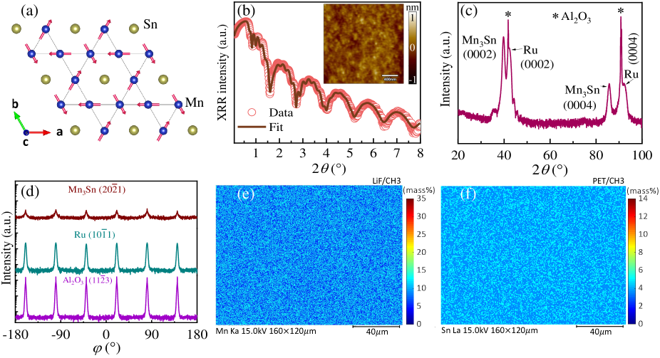
Mn3Sn has a hexagonal crystal structure, for which the (0001)-plane or the -plane has a kagome lattice as shown in Fig. 1(a). In order to grow the -plane Mn3Sn, we choose -plane sapphire (-Al2O3) substrate and a 7 nm thick Ru-seed layer. The films were grown using AJA Orion 8 magnetron sputtering system with a base pressure, better than Torr. First, the Ru seed layer was deposited at 400 ∘C and annealed at the same temperature for 10 minutes. Then the sample was allowed to cool to 100 ∘C, at which Mn3Sn was deposited by co-sputtering Mn and Sn targets. The Mn was deposited at a growth rate of 0.37 Å/s by applying 60 W DC power while the Sn was deposited at a growth rate of 0.20 Å/s by applying 40 W RF power. After the deposition of Mn3Sn layer, the sample was annealed in-situ at 600 ∘C for an hour. Subsequently, the sample was allowed to cool to room temperature, after which Ni80Fe20(8 nm)/Al(2 nm) was deposited without breaking the vacuum. The Al layer is used as the capping layer and is fully oxidized after exposure to air. During the deposition, we rotate the sample holder along its normal axis to ensure a uniform composition and thickness. The structural characterization was performed using high resolution X-ray diffraction (HR-XRD), while the growth rate and interfacial roughness were determined via X-ray reflectivity (XRR) measurements using a PANalytical x-ray diffractometer equipped with Cu Kα ( = 1.5406 Å) source. The morphology and surface roughness was determined by atomic force microscopy (AFM) scans (Asylum Research, MFP-3D system). The AFM images were obtained in the tapping mode using Asylum Research Probes (AC240TS-R3) cantilevers. The SHIMADZU (EPMA -1720 HT) electron probe microanalyzer (EPMA) system was used to determine the composition. A broadband ferromagnetic resonance (FMR) spectroscopy technique was used to characterize the magnetization dynamics of Mn3Sn/Ni80Fe20 bilayers. Field modulation technique with lock-in based detection is employed to enhance the sensitivity of FMR measurements. Kumar et al. (2019) The excitation radio frequency (RF) was varied from 3 to 8 GHz. To detect the ISHE voltage, copper pads were pasted beneath the inverted sample following the method used in our earlier work by Kumar Kumar et al. (2018)
Figure 1(b) shows the XRR measurement of the Al2O3/Ru(7 nm)/Mn3Sn(30 nm)/AlOx(2 nm) thin film. The thickness of Mn3Sn is extracted from the XRR fit, from which we determine the growth rate to be 0.48 Å/s. We obtained a low roughness ( 0.28 nm) from the fit of the XRR data. The AFM surface morphology also showed a lower root mean square roughness of 0.15 nm measured over a scan area of mm as shown in the inset. Figure 1(c) shows the corresponding 2- XRD pattern, showing the (0002)-peaks corresponding to both Mn3Sn and Ru seed layer. We also observe several satellite peaks (thickness fringes), indicating smooth interfaces and uniform film growth, which is also consistent with sharp Kiessig fringes observed in the XRR measurements [Fig. 1(b)]. We only observed (0002) and (0004) Mn3Sn peaks, indicating that a -plane oriented epitaxial Mn3Sn film has been achieved on the Ru seed layer. To determine the epitaxial relationship, we performed -scans for the peaks: Al2O3 (113) (violet), Ru (101) (cyan) and Mn3Sn (201) (wine) as presented in Fig. 1(d). The -scan clearly shows that a reflection appears periodically every 60∘ for Al2O3, Ru, and Mn3Sn, indicating that we have obtained non-twinned, highly epitaxial films. The location of the peaks indicates that the epitaxial film is formed with a relationship of Mn3Sn (0001)[200] || Ru (0001)[100] || Al2O3 (0001)[110], which is similar to the work by S. Kurdi et al. Kurdi et al. (2020)
In order to determine the composition and its distribution, we used an electron probe microanalyzer (EPMA) and energy dispersive X-ray (EDX) mapping on our samples. The composition of the film is estimated to be Mn3.14±0.03Sn0.86±0.01 using EDX mapping and Mn3.12±0.02Sn0.88±0.01 by quantitative analysis using EPMA system. Both measurements show the presence of excess Mn, which is known to be essential for the formation of the D019 Mn3Sn. Higo et al. (2018b) Figure 1(e) and (f) provide the elemental distribution maps of Mn and Sn atoms, respectively, showing that the elements are uniformly distributed. We measured the longitudinal resistivity of Ru(7 nm)/Mn3Sn(30 nm) bilayer using four point probe method to be 570 -cm.
Magnetization () measurement performed using superconducting quantum interference device (SQUID) on a 30 nm thick Mn3Sn thin film is shown in Fig. 2(a). It shows a weak magnetic moment of around 2 m/Mn at room temperature, which is lower than polycrystalline films, as well as reported results on -plane Mn3Sn thin films. Higo et al. (2018b); Ikeda et al. (2020) Magnetization () measurement for Mn3Sn/Ni80Fe20 (8 nm) bilayer is shown in the inset of Fig. 2(a), from which we determine saturation magnetization of Ni80Fe20 to be 750 emu/cc. In Fig. 2(b), we show example FMR spectra of Al2O3/Ru/Mn3Sn()/Ni80Fe20/AlOx for various thicknesses, of Mn3Sn measured at 4 GHz. The FMR data is fitted Celinski et al. (1997) to extract the values of half-width at half maximum (HWHM) or linewidth () and resonance field ().
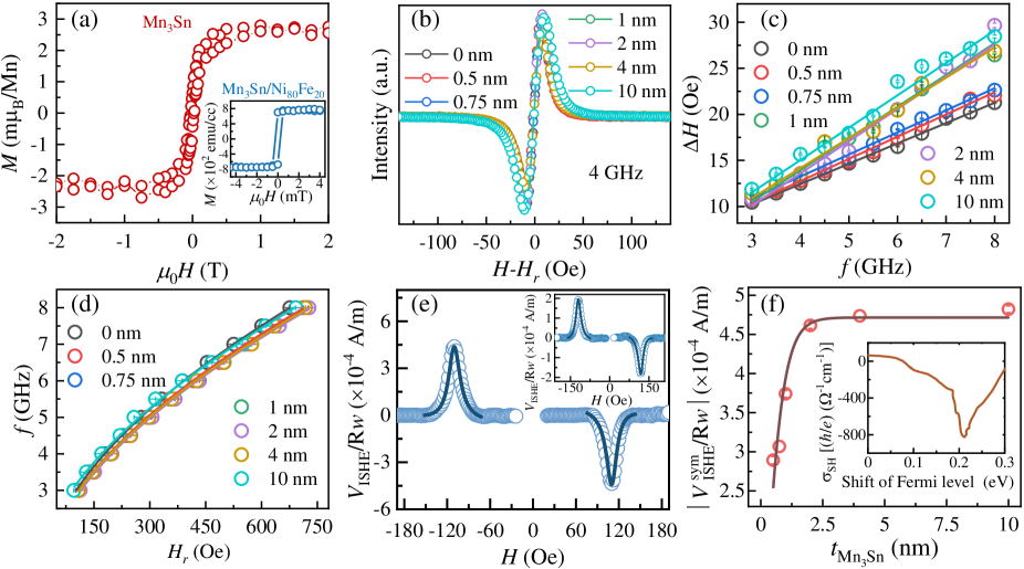
The vs. frequency () dependence of all the samples are plotted in Fig. 2(c). The measured data is fitted using following equation:
| (1) |
where is the effective Gilbert damping parameter, GHz/T is the gyromagnetic ratio, and is the inhomogeneous line broadening. The first term on the right hand side is the viscous damping of magnetization motion, while the second term is due to magnetic inhomogeneity and sample imperfections of the FM layer. Farle (1998) The slope of the linear fit using Eq. 1 is proportional to . As can be observed from Fig. 2(c), the slope of Mn3Sn()/Ni80Fe20(8 nm) is higher compared to its corresponding reference Ni80Fe20(8 nm) sample, which indicates spin current being pumped from Ni80Fe20 into Mn3Sn. Further, the low values of ( 3 Oe) from the fits indicate the high quality of our samples. Figure 2(d) shows the dependent (open circles) for various with their corresponding fit (solid line) using Kittel’s equation: Kittel (1948)
| (2) |
where is the uniaxial anisotropy field, and is the effective saturation magnetization. The is found to be comparable for all the Mn3Sn()/Ni80Fe20 samples and in the range of emu/cc, which is close to measured saturation magnetization of 750 emu/cc (estimated from magnetization measurements), indicating negligible perpendicular anisotropy.
Next, we performed the Mn3Sn thickness dependent ISHE measurements to determine the of our plane Mn3Sn films. Figure 2(e) shows a representative ISHE signal, (open circles) along with an ISHE signal measured from a Ta/Py/SiO2 sample (inset). To eliminate contribution from self-induced ISHE and other rectification effects from Ni80Fe20Gladii et al. (2019); Conca et al. (2017); Bangar et al. (2022), the signal from a reference (Ni80Fe20) sample is subtracted from the measured data. The sign of signal obtained from Mn3Sn agrees with Ta, indicating a negative sign of . The ISHE data () was fitted with a combination of symmetric () and asymmetric () components using equation: Deorani et al. (2014)
| (3) |
where is the applied magnetic field. The value of the symmetric part can be taken to be the spin pumping induced ISHE signal () in our geometry where rectification signals are minimized. Kumar et al. (2018) This is further supported by the fact that signal shape is entirely symmetric and the signal changes sign on reversal of field polarity, both of which are consistent with a dominant ISHE origin of the signal. Lustikova et al. (2015) Furthermore, in our geometry the magnetic field is perpendicular to the voltage measurement direction. For this condition, the magnetic spin Hall effect vanishes completely [see Fig. 3 (g) of Ref.Kimata et al., 2019]. Hence, in the following, we will not consider magnetic spin Hall effect or it’s inverse in Mn3Sn. The charge current generated due to ISHE in Mn3Sn can be written as , where is the resistance of the Mn3Sn/Ni80Fe20 bilayer. We further normalize the with the width () of the sample to eliminate any size effect. In order to determine and of Mn3Sn we plot with (Fig. 2(f)) and fit it with the following equation: Deorani et al. (2014)
| (4) |
where is the RF field generated due to the RF current of frequency flowing through the co-planar waveguide, is the saturation magnetization, is the reduced Planck’s constant, and is the electronic charge. From the fitting, we obtain the values of and to be 0.42 0.04 nm and -0.40 0.03, respectively. The is determined from the enhancement of damping using . Mosendz et al. (2010) The value is found to be m-2 at room temperature. This value of is comparable to the values reported for other systems such as Mn3Ga/CoFeB Singh et al. (2020) and Bi2Se3/Ni80Fe20 Deorani et al. (2014) and one order of magnitude higher than Ta/Ni80Fe20. Kumar et al. (2018) The value of is similar to the value reported for polycrystalline Mn3Sn. Muduli et al. (2019) The measured in our case is found to be rather large, especially considering the fact that Eq. 4 does not include interface transparency, which is less than one. Thus the values of -0.40 0.03 is a lower limit of . Our value of is greater than other antiferromagnets, such as 0.31 for polycrystalline Mn3Ga Singh et al. (2020) and 0.35 for (001)-oriented IrMn3. Zhang et al. (2016) In addition, the observed value of is considerably higher than the polycrystalline Mn3Sn value of 0.05, which was reported by one of the authors of this article using a non-local spin transport technique. Muduli et al. (2019) Our value is also more than twice that of Yu et al., Yu et al. (2021), where a value of was reported for polycrystalline Mn3Sn thin films interfaced with yttrium iron garnet.
In order to compare our results with theoretical calculations Zhang et al. (2018) of SHE in Mn3Sn, we determine using: , where is the charge conductivity of Ru/Mn3Sn bilayer, which was found to be 1754 cm-1, from four-point probe measurements. We found to be cm-1. Zhang et al. have predicted an intrinsic SHE in Mn3Sn that arises due to the non-collinear magnetic structure. They predicted cm-1 at the Fermi level. Our value is significantly larger and has the opposite sign, which can be explained if we assume the Fermi level is shifted in our thin films due to slightly higher Mn content. In fact, the band structure is found to be dominated by Mn- orbitals near the Fermi level Kuroda et al. (2017) and hence, an excess 3% Mn concentration (Mn3.12Sn0.88) in our samples can induce electron doping leading to a shift in the Fermi level. Such shift in Fermi level is already reported in Mn3Sn both by first principle calculations as well as by angle-resolved photoemission spectroscopy (ARPES) measurements. Kuroda et al. (2017) Based on the measured resistivity and using a scattering time of fs from Ref Cheng et al. (2019), we calculated a shift of about 0.09 eV (w.r.t. stoichiometric Mn3Sn with no excess Mn) which can easily lead to a sign change in , as shown in the inset of Fig. 2(f). However, this can not explain the large magnitude of , indicating that other extrinsic mechanisms may also contribute to .
In conclusion, we have demonstrated epitaxial growth of -plane oriented non-collinear antiferromagnet Mn3Sn with Ru as a seed layer on Al2O3 substrates. We have investigated ISHE in the -plane Mn3Sn/Ni80Fe20 system. Through Mn3Sn thickness dependent ISHE measurements, we determine key parameters like and for -plane Mn3Sn. We found a large of cm-1, which is higher than other non-collinear antiferromagnets reported till date. The results are important for spin-orbit torque-based spintronics devices utilizing non-collinear antiferromagnets.
Acknowledgements.
The partial support from the Ministry of Human Resource Development under the IMPRINT program (Grant no: 7519 and 7058), the Department of Electronics and Information Technology (DeitY), Science & Engineering research board (SERB File no. CRG/2018/001012), Joint Advanced Technology Centre at IIT Delhi, and Department of Science and Technology under the Nanomission program (grant no: ) are gratefully acknowledged. H.B. gratefully acknowledges the financial support from the Council of Scientific and Industrial Research (CSIR), Government of India.I AUTHOR DECLARATIONS
Conflict of Interest
The authors have no conflicts to disclose.
II DATA AVAILABILITY
The data that support the findings of this study are available from the corresponding author upon reasonable request.
References
- Han et al. (2018) W. Han, Y. Otani, and S. Maekawa, npj Quantum Mater. 3, 27 (2018).
- Žutić et al. (2004) I. Žutić, J. Fabian, and S. D. Sarma, Rev. Mod. Phys. 76, 323 (2004).
- Zhang et al. (2018) Y. Zhang, J. Železnỳ, Y. Sun, J. Van Den Brink, and B. Yan, New J. Phys. 20, 073028 (2018).
- Busch et al. (2021) O. Busch, B. Göbel, and I. Mertig, Phys. Rev. B 104, 184423 (2021).
- Nakatsuji et al. (2015) S. Nakatsuji, N. Kiyohara, and T. Higo, Nature 527, 212 (2015).
- Kondou et al. (2021) K. Kondou, H. Chen, T. Tomita, M. Ikhlas, T. Higo, A. H. MacDonald, S. Nakatsuji, and Y. Otani, Nat. Commun. 12, 6491 (2021).
- Ikhlas et al. (2017) M. Ikhlas, T. Tomita, T. Koretsune, M.-T. Suzuki, D. Nishio-Hamane, R. Arita, Y. Otani, and S. Nakatsuji, Nat. Phys. 13, 1085 (2017).
- Higo et al. (2018a) T. Higo, H. Man, D. B. Gopman, L. Wu, T. Koretsune, O. M. van’t Erve, Y. P. Kabanov, D. Rees, Y. Li, M.-T. Suzuki, et al., Nat. Photonics 12, 73 (2018a).
- Chen et al. (2014) H. Chen, Q. Niu, and A. H. MacDonald, Phys. Rev. Lett. 112, 017205 (2014).
- Kübler and Felser (2014) J. Kübler and C. Felser, EPL 108, 67001 (2014).
- Kimata et al. (2019) M. Kimata, H. Chen, K. Kondou, S. Sugimoto, P. K. Muduli, M. Ikhlas, Y. Omori, T. Tomita, A. MacDonald, S. Nakatsuji, et al., Nature 565, 627 (2019).
- Li et al. (2019) X. Li, C. Collignon, L. Xu, H. Zuo, A. Cavanna, U. Gennser, D. Mailly, B. Fauqué, L. Balents, Z. Zhu, et al., Nat. Commun. 10, 1 (2019).
- Takeuchi et al. (2021) Y. Takeuchi, Y. Yamane, J.-Y. Yoon, R. Itoh, B. Jinnai, S. Kanai, J. Ieda, S. Fukami, and H. Ohno, Nat. Mater. 20, 1364 (2021).
- Jungwirth et al. (2016) T. Jungwirth, X. Marti, P. Wadley, and J. Wunderlich, Nat. Nanotechnol. 11, 231 (2016).
- Baltz et al. (2018) V. Baltz, A. Manchon, M. Tsoi, T. Moriyama, T. Ono, and Y. Tserkovnyak, Rev. Mod. Phys. 90, 015005 (2018).
- Zhang et al. (2017) Y. Zhang, Y. Sun, H. Yang, J. Železný, S. P. P. Parkin, C. Felser, and B. Yan, Phys. Rev. B 95, 075128 (2017).
- Muduli et al. (2019) P. K. Muduli, T. Higo, T. Nishikawa, D. Qu, H. Isshiki, K. Kondou, D. Nishio-Hamane, S. Nakatsuji, and Y. Otani, Phys. Rev. B 99, 184425 (2019).
- Yu et al. (2021) T. Yu, H. Wu, H. He, C. Guo, C. Fang, P. Zhang, K. L. Wong, S. Xu, X. Han, and K. L. Wang, APL Mater. 9, 041111 (2021).
- Yoon et al. (2019) J. Yoon, Y. Takeuchi, R. Itoh, S. Kanai, S. Fukami, and H. Ohno, Appl. Phys. Express 13, 013001 (2019).
- Kumar et al. (2018) A. Kumar, R. Bansal, S. Chaudhary, and P. K. Muduli, Phys. Rev. B 98, 104403 (2018).
- Deorani and Yang (2013) P. Deorani and H. Yang, Appl. Phys. Lett. 103, 232408 (2013).
- Kumar et al. (2019) A. Kumar, N. Pandey, D. Kumar, M. Gupta, S. Chaudhary, and P. K. Muduli, Physica B: Condensed Matter 570, 254 (2019).
- Kurdi et al. (2020) S. Kurdi, P. Zilske, X. Xu, M. Frentrup, M. Vickers, Y. Sakuraba, G. Reiss, Z. Barber, and J. Koo, J. Appl. Phys. 127, 165302 (2020).
- Higo et al. (2018b) T. Higo, D. Qu, Y. Li, C. Chien, Y. Otani, and S. Nakatsuji, Appl. Phys. Lett. 113, 202402 (2018b).
- Ikeda et al. (2020) T. Ikeda, M. Tsunoda, M. Oogane, S. Oh, T. Morita, and Y. Ando, AIP Adv. 10, 015310 (2020).
- Celinski et al. (1997) Z. Celinski, K. Urquhart, and B. Heinrich, J. Magn. Magn. Mater. 166, 6 (1997).
- Farle (1998) M. Farle, Rep. Prog. Phys. 61, 755 (1998).
- Kittel (1948) C. Kittel, Phys. Rev. 73, 155 (1948).
- Gladii et al. (2019) O. Gladii, L. Frangou, A. Hallal, R. L. Seeger, P. Noël, G. Forestier, S. Auffret, M. Rubio-Roy, P. Warin, L. Vila, S. Wimmer, H. Ebert, S. Gambarelli, M. Chshiev, and V. Baltz, Phys. Rev. B 100, 174409 (2019).
- Conca et al. (2017) A. Conca, B. Heinz, M. Schweizer, S. Keller, E. T. Papaioannou, and B. Hillebrands, Phys. Rev. B 95, 174426 (2017).
- Bangar et al. (2022) H. Bangar, A. Kumar, N. Chowdhury, R. Mudgal, P. Gupta, R. S. Yadav, S. Das, and P. K. Muduli, ACS Appl. Mater. Interfaces , DOI:https://doi.org/10.1021/acsami.2c11162 (2022).
- Deorani et al. (2014) P. Deorani, J. Son, K. Banerjee, N. Koirala, M. Brahlek, S. Oh, and H. Yang, Phys. Rev. B 90, 094403 (2014).
- Lustikova et al. (2015) J. Lustikova, Y. Shiomi, and E. Saitoh, Phys. Rev. B 92, 224436 (2015).
- Mosendz et al. (2010) O. Mosendz, J. Pearson, F. Fradin, G. Bauer, S. Bader, and A. Hoffmann, Phys. Rev. Lett. 104, 046601 (2010).
- Singh et al. (2020) B. B. Singh, K. Roy, J. A. Chelvane, and S. Bedanta, Phys. Rev. B 102, 174444 (2020).
- Zhang et al. (2016) W. Zhang, W. Han, S.-H. Yang, Y. Sun, Y. Zhang, B. Yan, and S. S. Parkin, Sci. Adv. 2, e1600759 (2016).
- Kuroda et al. (2017) K. Kuroda, T. Tomita, M.-T. Suzuki, C. Bareille, A. Nugroho, P. Goswami, M. Ochi, M. Ikhlas, M. Nakayama, S. Akebi, et al., Nat. Mater. 16, 1090 (2017).
- Cheng et al. (2019) B. Cheng, Y. Wang, D. Barbalas, T. Higo, S. Nakatsuji, and N. Armitage, Appl. Phys. Lett. 115, 012405 (2019).