- \FAILED \FAILED
![[Uncaptioned image]](/html/2209.00815/assets/x1.png)
A 0.6 –1.8 Compact Temperature Sensor with 0.24 Resolution, 1.4 Inaccuracy and 1.06 per Conversion
Abstract
This paper presents a fully-integrated CMOS temperature sensor for densely-distributed thermal monitoring in systems on chip supporting dynamic voltage and frequency scaling. The sensor front-end exploits a sub-threshold PMOS-based circuit to convert the local temperature into two biasing currents. These are then used to define two oscillation frequencies, whose ratio is proportional to absolute-temperature. Finally, the sensor back-end translates such frequency ratio into the digital temperature code. Thanks to its low-complexity architecture, the proposed design achieves a very compact footprint along with low-power consumption and high accuracy in a wide temperature range. Moreover, thanks to a simple embedded line regulation mechanism, our sensor supports voltage-scalability. The design was prototyped in a 180 CMOS technology with a 0 100 temperature detection range, a very wide supply voltage operating range from 0.6 up to 1.8 and very small silicon area occupation of just 0.021 . Experimental measurements performed on 20 test chips have shown very competitive figures of merit, including a resolution of 0.24 , an inaccuracy of 1.4 , a sampling rate of about 1.5 and an energy per conversion of 1.06 at 30 .
1 Introduction
Temperature sensors are crucial to allow dynamic thermal management (DTM) in complex Systems on Chips (SoCs) [1, 2, 3, 4]. Multiple sensors are distributed across the die to identify potential hot/cold-spots, and the collected temperature information is used to keep the operation of the chip within the target thermal condition, thus ensuring both performance and reliability [2, 3, 4]. The temperature safety can be maintained while accommodating dynamic voltage and frequency scaling (DVFS), powering on/off different portions of the system and/or implementing other adaptive thermal adjustments like fan speed regulation [1, 5, 6].
Some proposed temperature sensors [7, 8, 9, 10, 11, 12, 13, 14, 15, 16, 17, 18, 19, 20] exhibit the required sensing accuracy for proper DTM. A typical requirement for multi-core systems is a modest absolute inaccuracy of 8 and a more constrained relative inaccuracy of 3 [8, 21]. Additional requirements are imposed by recent technology trends, such as multi-processor chips, 3-D integration and multi-supply voltage architectures [7]. Particularly:
-
1.
Small size is a highly desired feature to enable very dense thermal monitoring, as required in state-of-the-art VLSI designs. In fact, due to the ever-increasing level of integration of modern SoCs, the number of possible hot/cold-spots is rapidly growing with the consequent growth in the number of required temperature sensors for effective DTM (e.g., more than 60 in the POWER9 systems [5]). Moreover, a compact footprint is further important to ensure flexibility in the design process, since the optimal sensor locations (e.g., very close to the possible hot/cold-spots) often are identified only in the later stages of the design phase and, typically they are in very dense areas of the chip [8].
-
2.
Robustness is essential: A temperature sensor needs to maintain its sensing accuracy under voltage and process variations. In fact, overestimating the temperature can cause unnecessary performance throttling, while underestimating can lead to reliability issues.
-
3.
Broad supply voltage scalability is a further requirement [7]. Today’s SoCs often implement DVFS techniques to tune performance while managing power consumption, especially for digital portions of the system. The supply voltage can be dynamically modulated down to near threshold levels when reduced performance allows saving energy. It is therefore desirable that temperature sensors support supply voltage scalability in order to share the same power grids with the digital circuits. Unfortunately, some of the previously proposed temperature sensors turned out to be not enough voltage scalable [9, 11, 14, 15, 16, 19], and/or do not support sub-1 operation [8, 17, 22, 15, 16, 19].
This paper introduces a small-area fully-integrated CMOS temperature sensor, suitable for aggressive circuit placement (i.e., very close to target hot/cold-spots) in SoCs. A low-complexity PMOS-based sensing circuit converts the local temperature into two sub-threshold biasing currents. These are then used to define two oscillation frequencies, whose ratio increases linearly as the temperature rises. Such frequency ratio is then translated into a digital output code, through a digital back-end, based on binary counters. Thanks to a simple embedded line regulation mechanism, the proposed design can operate in a wide power supply range, thus resulting to be appealing for those systems which support multi-supply voltages and/or DVFS. When fabricated in 180 nm CMOS for the target 0 – 100 temperature range, our design exhibits a compact footprint of about 0.02 and a supply voltage operating range from 0.6 V to 1.8 V. Moreover, it consumes less than 1.6 (=0.6 V and =25 ), with an energy per conversion of 1.05 . The above results were achieved with an inaccuracy constrained within 1.4 , and a resolution of 0.24 .
The remainder of the paper is organized as follows. Section II details the temperature sensor design. Section III presents measurement results over 20 test samples. Section IV compares our proposal with some recent CMOS-based competitors proposed in the literature. Finally, Section V concludes the work.
2 Proposed Temperature Sensor
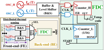
Inherited from the temperature-to-digital conversion methodology exploited in [14, 13], the sensor relies on three main processing blocks, as shown in Fig. 1. 1) The temperature-to-current converter (TCC) represents the sensing element of the proposed circuit. It generates two sub-threshold currents, and (with ), whose ratio has an increasing linear dependence with the temperature. 2) The current-to-frequency converter (CFC) consists of two independent ring oscillators controlled by mirrored and currents. The ratio of the two oscillation frequencies (i.e., /) is maintained linear with temperature. 3) Finally, the frequency-to-digital converter (FDC) generates the digital temperature code, based on the / ratio.
The voltage scalability of the sensor derives from two stacked native (i.e., zero threshold voltage transistors) NMOS devices [12], which provide line regulation for the supply-sensitive TCC and CFC blocks. Indeed, these are powered in the sub-threshold region by an almost stable virtual (), regardless of the actual and temperature. In our 180 implementation, the is about 440 across very large temperature (0 – 100 ) and power supply (0.6 – 1.8 ) variations. Differently, the FDC circuit, being based on not-critical digital circuitry (i.e., intrinsically more robust to temperature and voltage variations) is powered directly by the .
2.1 Temperature-to-Current Converter
The proportional-to-absolute-temperature (PTAT) behavior of the current ratio is obtained thanks to the low-complexity circuit shown in the inset of Fig. 2. Such circuit is organized in two branches, including only five diode-connected PMOS devices. The left (right) branch is implemented with 3 (2) identically sized transistors, so that the is equally partitioned between them resulting in (). Since all the devices of the TCC operate in the sub-threshold region, with a source-to-drain voltage, , larger than four thermal voltages = ( is the Boltzmann constant, is the absolute temperature, and is the electron charge), their source current can be expressed as [23]:
| (1) |
where is the aspect ratio of the device, is the technology dependent subthreshold current which can be obtained by extrapolating the current for , is the threshold voltage and is the subthreshold factor.
Thus, the current ratio can be written as:
| (2) |
where we have assumed that and for transistors M1 and M2 are the same.
Based on the value assumed by the term , the exponential can be well approximated by a linear relation in a bounded temperature range (e.g. 0 – 100 ), according to:
| (3) |
with = 16.1 , = 2.55 for our design, and expressed in . The obtained model equation (2) is plotted in Fig. 2, where it can be appreciated the good agreement with simulation results.
2.2 Current-to-Frequency Converter
As shown in Fig. 3(a), the CFC exploits two current-starved ring oscillators to convert the mirrored version of the and currents into two digital pulse signals, whose frequency ratio / maintains a linear PTAT trend.
In general, the oscillation period of a current-biased ring oscillator can be expressed as [13]:
| (4) |
where is the number of stages in the ring oscillator, is the load capacitance of a single delay cell, is the output voltage amplitude, is the biasing current, while and are the falling and the rising times of a single stage. Both and should be sufficiently small compared with so that the oscillation frequency can be approximated as proportional to . In this case, / ( ) provides a similar PTAT characteristic as /.
In our design, both the ring oscillators use the same delay cell topology (see Fig. 3(a)), based on a standard CMOS inverter loaded by a NMOS capacitor. The latter limits the oscillation frequency, while avoiding excessive increasing in the number of delay cells. As an additional benefit, the added capacitance at the output node of each inverter helps in increasing the linearity of the oscillation frequency with the biasing current (as from (4)). The two ring oscillators have been designed with a proper number of stages (13 and 7 for the slow and the fast oscillators, respectively) and delay stage sizing. As shown in Fig. 3(a), decoupling MIM capacitors (400 ) were introduced at the supply voltage nodes of the two oscillators to reduce the impact of the switching noise on the oscillation frequency.
Simulation results of the FDC circuit driven by the TCC are shown in Fig. 3(b-c). From Fig. 3(b), as temperature increases from 0 to 100 , () spans from 17 (4.3 ) to 31.8 (9.6 ). As shown in Fig. 3(c), the adjusted- of 0.99995, evaluated on the / ratio, leads to a tolerable error after a two-point calibration, with 10 and 90 as temperature references.
2.3 Voltage Regulation
A low-complexity voltage regulation mechanism has been implemented to improve line and temperature sensitivities of TCC and CFC blocks. This has been achieved by interposing two series-connected native NMOS devices between and the TCC+CFC circuits, as depicted in Fig. 1. In this way, the source of the lower native transistor corresponds to the virtual supply voltage seen by the TCC and CFC blocks. Note that, the stack of two native transistors will always be operated in sub-threshold, given that both have and . The use of two long channel transistors in series to implement the voltage regulator block, makes its characteristic essentially insensitive to variations of the external . Moreover, such approach also leads to an almost stable with temperature variations. In order to better explain this, we rely on the scheme reported in Fig. 4, where the regulator (REG) and the TCC and CFC circuits (LOAD) are modeled independently. For the regulator, an characteristic in the following form is assumed:
| (5) |
in which the DIBL effect is neglected (i.e., the impact on ).
Such a kind of regulator is capable to provide an almost constant to a load a circuit whose relation can be expressed in the following form:
| (6) |
which is reasonable for CMOS circuits operated in sub-threshold regime, such as the TCC and CFC blocks in our design.
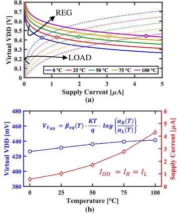
In Fig. 5(a), the DC V-I curves for regulator and load, simulated at different temperatures, are depicted. The analytical expression of these curves can be easily obtained by writing (5) and (6) in their respective logarithmic forms. The crossing points between the two curve families represent the load conditions for different temperatures. From this plot, it can be easily understood how the is essentially stable as temperature changes, despite the supply current exponentially increases with temperature.
| (8) |
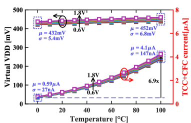
in which all the terms , , and are individually a function of the temperature. In fact, we have verified that the ratio is essentially constant, while the term has an almost 1/T dependence which compensates the linear term in . The aforementioned fitting parameters have been extracted for the regulator and load circuits at the different temperatures, and the corresponding analytical expression for and the supply current are reported in Fig. 5(b): when the temperature raises from 0 to 100 , although an about 7 times current increase is observed, the corresponding change in the voltage is of about 3%. The extracted model equations are consistent with the sensor front-end simulations reported in Fig. 6, which shows the behavior of voltage node and current drawn by the front-end (stacked native NMOS devices biasing TCC and CFC) sensor circuitry as a function of temperature for ranging from 0.6 to 1.8 with a step of 100 . It can be easily observed that while the average current increases from about 0.6 @ T= 0 to 4.1 @ T= 100 (i.e., drawn current increases more than 6.9 times as temperature passes from 0 to 100 ), the increases of less than 5% in the same temperature range. At the same time, stays quite constant for spreading from 0.6 to 1.8 , as a consequence of long channel stacked NMOS devices used to screen the dependence. From the above considerations, are then evident the benefits of the adopted low-complexity voltage regulation to improve both line and temperature sensitivities.
In deeply scaled process nodes (i.e. below 40-nm), native MOSFETs could not be available. In this case, the described voltage regulation can be realized by properly sized nMOS devices with regular (RVT), as long as they are biased with a stable gate voltage close to the , so that the leads them to operate in the sub-threshold regime.
2.4 Frequency-to-Digital Converter
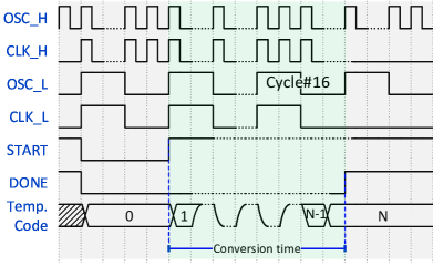
The principle scheme of the digital back-end, responsible for generating the digital PTAT code, is shown in Fig. 7. Since the amplitude of the signals produced by the two ring oscillators in the CFC is constrained by the voltage level, both signals are up-converted to the voltage domain by the compact and energy-efficient level shifter (LS) proposed in [24]. Such circuit exhibits a very large voltage conversion range, and it is adaptive to change in voltage level [24], rendering the whole temperature sensor fully compatible with DVFS systems. Frequency to digital conversion is then performed by two asynchronous counters. The acts as reference counter to set the time window of the temperature measurement sampling. This 5-bit counter defines a sampling time window of 16/ seconds, since only 4 bits are used for counting while the MSB is exploited for triggering purpose. On the other side the resolution of the temperature sensor depends on , which was sized for 13-bit to prevent counting overflow over the temperature detection range from 0 to 100 , also considering some margin against undesired offsets due to process/mismatch variations.
The timing diagram of the FDC block is shown in Fig. 8. When the START signal is triggered (note that, the START and the signals are synchronized), both counters begin counting upward until the transition to ’1’ of the DONE signal (i.e., the MSB of the reference counter), which happens after sixteen cycles of the slower oscillator. At this time, a temperature code is available at the output of the . Both the counters are reset by the START signal when a new temperature measurement is required.
In a general system, the FDC circuit can be shared between multiple sensor front-ends as shown in the sketch in Fig. 7. In this case, the back-end comprises two n-to-1 multiplexers, which take n output pairs from different sensor front-ends (i.e. each pair consists of the two signals at and frequencies) and pass the selected pair to the shared FDC. This allows to save precious silicon area when multiple thermal information is required for an effective DTM.
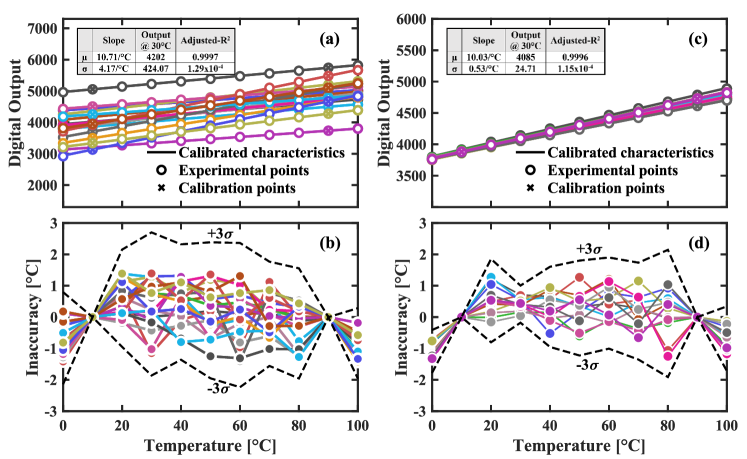
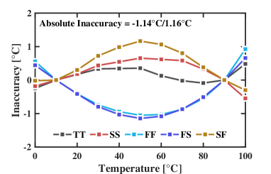
Fig. 9 reports simulated inaccuracy for the output temperature code in the target temperature detection range while considering different process corners and two-point calibration with 10 and 90 as temperature references. An absolute inaccuracy of –1.14 1.16 is observed at 50 for the FS/SF corners. Such result suggests a low susceptibility of the proposed design against process variability.
3 Experimental Results
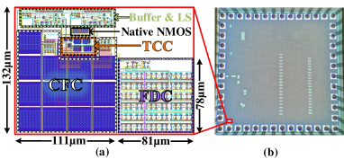
The fully-integrated temperature sensor was fabricated in a 180 CMOS technology node, while occupying a very small silicon area (less than 0.021 ). The physical design is shown in Fig. 10(a), whereas a micrograph of the test chip is reported in Fig. 10(b). A silicon area of 14650 is occupied by the voltage-regulated sensor front-end, while the FDC footprint requires about 6300 .
Twenty test chips were measured in the target temperature range considering two-point calibration, with 10 and 90 as temperature references. Obtained results are summarized in Fig. 11. More precisely, Fig. 11(a) reports the temperature code of measured chips calibrated for =600 . A very good linearity was found for all the samples with an average adjusted- of 0.9997, which is only slightly degraded with respect to that observed from the simulation results (see Fig. 3(c)). However, from Fig. 11(a), a noticeable difference can be appreciated in the slope coefficient from sample to sample. This prevents a simple 1-point calibration to be exploited when significantly high accuracy in the measurement must be guaranteed. The inaccuracy of the measurements as a function of the temperature is shown in Fig. 11(b). For all the measured samples, the inaccuracy is always maintained within the –1.45 /1.4 range. Also looking to the pessimistic 3 data (about 2.5 ), such measurement results are well within the acceptable accuracy specs for an effective DTM in state-of-the-art SoC [8, 21]. Additional measurements performed on a single sensor are reported in Fig. 11(c-d). Here, the effect of voltage scaling was evaluated by considering a sweep on the from 0.6 to 1.8 with 100 step. Note that, for each supply voltage, an independent two-point calibration was considered. From Fig. 11(c), it can be observed that the digital temperature code differs significantly only at the highest temperatures, whereas, as shown in Fig. 11(d), the inaccuracy spans from –1.35 @ = 1.5 to 1.27 @ = 0.8 . The 3 inaccuracy is within the 2 range.
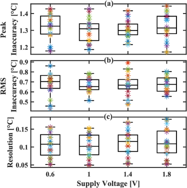
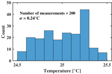
Die-to-die variability in the target temperature detection range is fully evaluated in Fig. 12(a-c), by considering all test samples and 4 different supply voltage values (i.e., =0.6 , 1 , 1.4 and 1.8 ). From Fig. 12(a), the peak inaccuracy is within a range of 1.1 1.45 , with a median value close to 1.3 . This corresponds to a RMS inaccuracy in the range from 0.42 to 0.89 , as shown in Fig. 12(b). Whereas the achieved resolution (i.e., the inverse slope of the sensor output characteristics) shows very competitive values with a worst case of 0.22 for = 1.8 , as reported in Fig. 12(c). The measured average resolution is 0.132 , 0.131 , 0.138 and 0.139 for equal to 0.6 , 1 , 1.4 and 1.8 , respectively. Indeed, the sampled temperature code can change in each measurement due to thermal noise. To properly evaluate the sensor resolution, the temperature code was measured 200 times at the fixed temperature of 25 for a typical sample. Fig. 13 reports the result of this experiment. The standard deviation of the samples is 0.24 (i.e. the noise-limited resolution), which corresponds to 1.84 LSB.
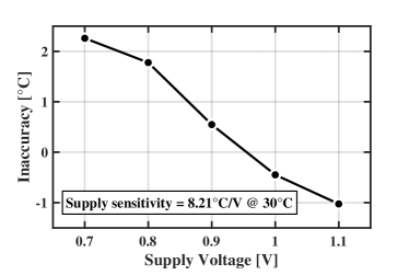
Sensitivity to unwanted voltage variations for the typical sample is characterized in Fig. 14, which shows inaccuracy as a function of supply voltage. A line sensitivity of 8.21 / at a temperature of 30 was measured by calibrating the sensor only at 0.9 and then extracting the inaccuracy when supply changes in the 200 (i.e., 22%) range. However, when supply voltage of the sensor is changed as an effect of DVFS adjustment, the line sensitivity can be further reduced down to 0.56 / at 30 . In fact, in this case, the two temperature calibration points for each possible (i.e. within the chip operating range) can be easily pre-stored to define the actual calibrated characteristic (see Fig. 11(d)).
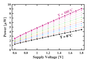
Finally, Fig. 15 shows the power consumption of the proposed sensor as a function of for temperature ranging from 0 to 100 . Power increases almost linearly with the , spreading from 1.57 ( = 0.6 ) to 5.61 ( = 1.8 ) at 25 . On the other side, power also increases with the temperature, reaching a maximum value of about 9 (= 1.8 and = 100 ).
4 Comparison
Table 1 summarizes measurement results of the temperature sensor as compared to alternative CMOS designs [9, 10, 13, 11, 8, 14, 15, 16, 19, 25, 26]. Experimental results provided for our design come from measurements on 20 test chips, while that of most of the competitors are based on a smaller number of samples (except for [8] and [26]). The circuits reported in [8, 15, 16, 19] do not support operation with sub 1 voltages, while sensors discussed in [9, 14, 15, 16] show poor voltage scalability. On the contrary, our sensor supports the larger supply voltage operating range from 0.6 to 1.8 , while exhibiting a supply sensitivity of about 8 / . In addition, it does not require any external reference signal unlike the circuits reported in [25] and [26], which use a reference clock [26] and a reference voltage [25], respectively. Moreover, the proposed design exhibits a relatively small footprint of just 0.021 . Indeed, it turns out to be the less area-hungry design in 180 and the third in absolute terms.
|
|
|
|
|
|
|
|
|
|
|
This work | |||||||||||||||||||||||
| Technology [nm] | 130 | 65 | 180 | 130 | 65 | 180 | 130 | 65 | 55 | 65 | 180 | 180 | ||||||||||||||||||||||
| Measured Samples | 7 | 7 | 8 | 10 | 12 | 9 | 9 | 35 | 64 | 9 | 9 | 20 | ||||||||||||||||||||||
|
No |
|
No |
|
|
Yes | No |
|
|
|
No |
|
||||||||||||||||||||||
|
1.2 | 1 | 1.8 | 1.2 | 0.5 | 0.8 | 0.95 | 1.2 | 0.9 | 0.8 | 0.35 | 0.6 | ||||||||||||||||||||||
| Area [mm2] | 0.031 |
|
0.118 | 0.06 | 0.63 | 0.074 | 0.07 | 0.0019 |
|
0.32 | 0.049 |
|
||||||||||||||||||||||
|
20 – 120 | 0 – 100 | -20 – 120 | -20 – 100 | 0 – 100 | -20 – 80 | 0 – 80 | -10 – 100 | -40 – 125 | -30 – 70 | 0 – 100 | 0 – 100 | ||||||||||||||||||||||
|
Yes | Yes | No | No (Yes) | No | No | Yes | Yes | Yes | No | No | No | ||||||||||||||||||||||
| Calibration | 1-point | 2-point | 2-point | 1-point | 2-point | 2-point | 2-point | 2-point | 2-point | 2-point | 2-point | 2-point | ||||||||||||||||||||||
| Min/Max Inaccuracy [°C] | -0.63/1.04 | -0.9/0.9 | -1.5/1.71 |
|
-1.53/1.61 | -0.9/1.2 | -0.4/0.44 | -1.62/2.04 | -0.37/0.72 | -1/0.7 | -3/3 | -1.45/1.4 | ||||||||||||||||||||||
|
1.67 | 1.8 | 2.86 | 4.66 (2.55) | 3.14 | 2.1 | 1.05 | 4.54 | 0.66 | 1.7 | 6 | 2.85 | ||||||||||||||||||||||
| Resolution [°C] | 0.595(e) | 0.3(f) | 0.048(f) | 0.34(e) | 0.3(e) | 0.145(f) | 0.1(e) | 0.32(f) | 0.013(f) | 0.075(e) | 0.27(e) |
|
||||||||||||||||||||||
|
0.0023 | 0.022 | 1 | 0.0133 | 300 | 839 | 59 | 0.01 | 1.3 | 765 | 33 |
|
||||||||||||||||||||||
|
0.67 | 3.4 | 93.6 | 9.92 | 0.23 | 8.9 | 11.56 | 0.94 | 12.8 | 4.9 | 0.46 |
|
||||||||||||||||||||||
| R-FoM [nJK2] | 0.237 | 0.3 | 0.216 | 1.147 | 0.02 | 0.19 | 0.116 | 0.096 | 0.022 | 0.028 | 0.033 | 0.061 | ||||||||||||||||||||||
|
43(d) | 34 | - | 13.6 | 8.4 | 3.8 | 13.7 | 2.4 | 5.76 | 2.8 | 16 | 8.21 | ||||||||||||||||||||||
| Power [W] | 288µ |
|
93.6µ | 744µ |
|
|
|
94µ | 9.3µ | 6.4n |
|
|
-
(b) Relative Inaccuracy = (Max Inaccuracy – Min Inaccuracy)/Temperature Range × 100. (d) Simulated result. (f) Noise-limited resolution.
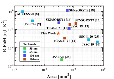
After a two-point calibration (i.e., with 10 and 90 as temperature calibration references), our sensor has a relative and a peak inaccuracy of 2.85% and of about 1.4 , respectively (both well within the required specs for multi-core systems [8, 21]) in the 0 100 temperature range. Such results are achieved without the need for additional non linearity correction logic, while exhibiting a noise limited resolution of 0.24 and an energy per conversion of only 1.06 nJ. Above results lead to a competitive resolution figure-of-merit (R-FoM), defined as [27]. This can be graphically appreciated in Fig. 16, which shows the R-FoM/area trade-off for the compared designs. Reported results put our sensor in a position, where none of the competitors perform better in both
5 Conclusions
In this paper, we propose a fully-integrated CMOS temperature sensor suitable for dense thermal monitoring in advanced SoC. Its low-complexity circuit topology allows compact footprint and voltage scalability along with low-power consumption and high accuracy in a large temperature range. The sensor was fabricated in 180 CMOS standard technology and experimentally characterized demonstrating competitive performance with respect to the state-of-the-art.
References
- [1] X. Li, Z. Li, W. Zhou, and Z. Duan, “Accurate on-chip temperature sensing for multicore processors using embedded thermal sensors,” IEEE Transactions on Very Large Scale Integration (VLSI) Systems, vol. 28, no. 11, pp. 2328–2341, 2020.
- [2] J. Long, S. O. Memik, G. Memik, and R. Mukherjee, “Thermal monitoring mechanisms for chip multiprocessors,” ACM Trans. on Architecture and Code Optimization (TACO), vol. 5, no. 2, pp. 1–33, 2008.
- [3] X. Li, X. Wei, and W. Zhou, “Heuristic thermal sensor allocation methods for overheating detection of real microprocessors,” IET Circuits, Devices & Systems, vol. 11, no. 6, pp. 559–567, 2017.
- [4] A. N. Nowroz, R. Cochran, and S. Reda, “Thermal monitoring of real processors: Techniques for sensor allocation and full characterization,” in Design Automation Conference. IEEE, 2010, pp. 56–61.
- [5] C. Gonzalez, E. Fluhr, D. Dreps, D. Hogenmiller, R. Rao, J. Paredes, M. Floyd, M. Sperling, R. Kruse, V. Ramadurai et al., “3.1 POWER9™: A processor family optimized for cognitive computing with 25Gb/s accelerator links and 16Gb/s PCIe Gen4,” in 2017 IEEE International Solid-State Circuits Conference (ISSCC). IEEE, 2017, pp. 50–51.
- [6] J. S. Shor and K. Luria, “Miniaturized BJT-Based Thermal Sensor for Microprocessors in 32- and 22-nm Technologies,” IEEE Journal of Solid-State Circuits, vol. 48, no. 11, pp. 2860–2867, 2013.
- [7] T. Yang, S. Kim, P. R. Kinget, and M. Seok, “Compact and Supply-Voltage-Scalable Temperature Sensors for Dense On-Chip Thermal Monitoring,” IEEE J. Solid-State Circuits, vol. 50, no. 11, pp. 2773–2785, 2015.
- [8] N. Vinshtok-Melnik and J. Shor, “Ultra Miniature Ring Oscillator Based Temperature Sensor,” IEEE Access, vol. 8, pp. 91 415–91 423, 2020.
- [9] T. Anand, K. A. Makinwa, and P. K. Hanumolu, “A VCO based highly digital temperature sensor with 0.034° C/mV supply sensitivity,” IEEE Journal of Solid-State Circuits, vol. 51, no. 11, pp. 2651–2663, 2016.
- [10] H. Wang and P. P. Mercier, “A 763 pW 230 pJ/conversion fully integrated CMOS temperature-to-digital converter with+ 0.81° C/- 0.75° C inaccuracy,” IEEE J. Solid-State Circuits, vol. 54, no. 8, pp. 2281–2290, 2019.
- [11] J. Li, Y. Lin, N. Ning, and Q. Yu, “A+ 0.44° C/- 0.4° C Inaccuracy Temperature Sensor With Multi-Threshold MOSFET-Based Sensing Element and CMOS Thyristor-Based VCO,” IEEE Trans. Circuits Syst. I: Regular Papers, vol. 68, no. 3, pp. 1102–1113, 2021.
- [12] K. Yang, Q. Dong, W. Jung, Y. Zhang, M. Choi, D. Blaauw, and D. Sylvester, “9.2 A 0.6 nJ- 0.22/+ 0.19 C inaccuracy temperature sensor using exponential subthreshold oscillation dependence,” in 2017 IEEE Int. Solid-State Circuits Conference (ISSCC). IEEE, 2017, pp. 160–161.
- [13] T. Someya, A. M. Islam, T. Sakurai, and M. Takamiya, “An 11-nW CMOS Temperature-to-Digital Converter Utilizing Sub-Threshold Current at Sub-Thermal Drain Voltage,” IEEE J. Solid-State Circuits, vol. 54, no. 3, pp. 613–622, 2019.
- [14] B. Zambrano, E. Garzón, S. Strangio, F. Crupi, and M. Lanuzza, “A 0.05 mm², 350 mV, 14 nW Fully-Integrated Temperature Sensor in 180-nm CMOS,” IEEE Trans. Circuits Syst. II: Express Briefs, vol. 69, no. 3, pp. 749–753, 2022.
- [15] Q. Huang, H. Joo, J. Kim, C. Zhan, and J. Burm, “An energy-efficient frequency-domain CMOS temperature sensor with switched vernier time-to-digital conversion,” IEEE Sens. J., vol. 17, no. 10, pp. 3001–3011, 2017.
- [16] Y.-J. An, K. Ryu, D.-H. Jung, S.-H. Woo, and S.-O. Jung, “An Energy Efficient Time-Domain Temperature Sensor for Low-Power On-Chip Thermal Management,” IEEE Sensors Journal, vol. 14, no. 1, pp. 104–110, 2014.
- [17] M. Jalalifar and G.-S. Byun, “A Wide Range CMOS Temperature Sensor With Process Variation Compensation for On-Chip Monitoring,” IEEE Sensors Journal, vol. 16, no. 14, pp. 5536–5542, 2016.
- [18] A. Azam, Z. Bai, and J. S. Walling, “An Ultra-Low Power CMOS Integrated Pulse-Width Modulated Temperature Sensor,” IEEE Sensors Journal, vol. 21, no. 2, pp. 1294–1304, 2021.
- [19] Z. Tang, N. N. Tan, Z. Shi, and X.-P. Yu, “A 1.2V Self-Referenced Temperature Sensor With a Time-Domain Readout and a Two-Step Improvement on Output Dynamic Range,” IEEE Sensors Journal, vol. 18, no. 5, pp. 1849–1858, 2018.
- [20] C.-C. Hung and H.-C. Chu, “A Current-Mode Dual-Slope CMOS Temperature Sensor,” IEEE Sens. J., vol. 16, no. 7, pp. 1898–1907, 2016.
- [21] Y. W. Li, H. Lakdawala, A. Raychowdhury, G. Taylor, and K. Soumyanath, “A 1.05 1.6 0.45 3-resolution -based temperature sensor with parasitic-resistance compensation in 32 CMOS,” in 2009 IEEE International Solid-State Circuits Conference - Digest of Technical Papers, 2009, pp. 340–341,341a.
- [22] S. Hwang, J. Koo, K. Kim, H. Lee, and C. Kim, “A 0.008 500 469 kS/s Frequency-to-Digital Converter Based CMOS Temperature Sensor With Process Variation Compensation,” IEEE Trans. Circuits Syst. I: Regular Papers, vol. 60, no. 9, pp. 2241–2248, 2013.
- [23] M. Alioto, “Ultra-Low Power VLSI Circuit Design Demystified and Explained: A Tutorial,” IEEE Transactions on Circuits and Systems I: Regular Papers, vol. 59, no. 1, pp. 3–29, 2012.
- [24] M. Lanuzza, F. Crupi, S. Rao, R. De Rose, S. Strangio, and G. Iannaccone, “An ultralow-voltage energy-efficient level shifter,” IEEE Trans. Circuits Syst. II: Express Briefs, vol. 64, no. 1, pp. 61–65, 2016.
- [25] T. Someya, A. K. M. M. Islam, and K. Okada, “A 6.4 nW 1.7% Relative Inaccuracy CMOS Temperature Sensor Utilizing Sub-Thermal Drain Voltage Stabilization and Frequency-Locked Loop,” IEEE Solid-State Circuits Letters, vol. 3, pp. 458–461, 2020.
- [26] Z. Tang, Y. Fang, Z. Shi, X.-P. Yu, N. N. Tan, and W. Pan, “A 1770- m2 Leakage-Based Digital Temperature Sensor With Supply Sensitivity Suppression in 55-nm CMOS,” IEEE Journal of Solid-State Circuits, vol. 55, no. 3, pp. 781–793, 2020.
- [27] K. A. A. Makinwa, “Smart Temperature Sensor Survey.” [Online]. Available: http://ei.ewi.tudelft.nl/docs/TSensor_survey.xls
[![[Uncaptioned image]](/html/2209.00815/assets/AuthorPhotosBio/BZ.jpg) ]Benjamin Zambrano
received the B.E degree in electronics from Escuela Superior Politecnica del Litoral, Guayaquil, Ecuador, in 2015, and a double M.S degree in nanoelectronics and electronics from University San Francisco de Quito, Ecuador, and University of Calabria, Rende, Italy, respectively, in 2020.
He is currently pursuing the Ph.D degree in ICT with the University of Calabria.
His research interests include integrated temperature sensors, ultralow-power/voltage designs and analog-based machine learning circuits.
]Benjamin Zambrano
received the B.E degree in electronics from Escuela Superior Politecnica del Litoral, Guayaquil, Ecuador, in 2015, and a double M.S degree in nanoelectronics and electronics from University San Francisco de Quito, Ecuador, and University of Calabria, Rende, Italy, respectively, in 2020.
He is currently pursuing the Ph.D degree in ICT with the University of Calabria.
His research interests include integrated temperature sensors, ultralow-power/voltage designs and analog-based machine learning circuits.
[![[Uncaptioned image]](/html/2209.00815/assets/AuthorPhotosBio/EG.jpg) ]Esteban Garzón
(S’14) received his B.Sc. degree in electronics engineering from Univ. San Francisco de Quito (USFQ), Ecuador, in 2016, and a double M.Sc. degree in nanoelectronics and electronics from USFQ and Univ. of Calabria (UNICAL), Italy, respectively, in 2018.
He is currently pursuing his Ph.D degree in the department of Computer Engineering, Modeling, Electronics and Systems Engineering, UNICAL, Italy.
He has authored/co-authored more than 25 scientific papers in international journals and conferences.
His research interests cover spin electronics/spintronics, cryogenic electronics, and emerging technologies for logic and memory low-power applications.
]Esteban Garzón
(S’14) received his B.Sc. degree in electronics engineering from Univ. San Francisco de Quito (USFQ), Ecuador, in 2016, and a double M.Sc. degree in nanoelectronics and electronics from USFQ and Univ. of Calabria (UNICAL), Italy, respectively, in 2018.
He is currently pursuing his Ph.D degree in the department of Computer Engineering, Modeling, Electronics and Systems Engineering, UNICAL, Italy.
He has authored/co-authored more than 25 scientific papers in international journals and conferences.
His research interests cover spin electronics/spintronics, cryogenic electronics, and emerging technologies for logic and memory low-power applications.
[![[Uncaptioned image]](/html/2209.00815/assets/AuthorPhotosBio/SS.jpg) ]Sebastiano Strangio
(Member, IEEE) was with the University of Udine, Udine, Italy, as a Temporary Research Associate, from 2013 to 2016, and with Forschungszentrum Jülich, Jülich, Germany, as a Visiting Researcher in 2015. From 2016 to 2019, he was with LFoundry, Avezzano, Italy. He is a Researcher in electronics at the University of Pisa, Pisa, Italy. He has authored and coauthored over 30 articles. His research interests include technologies for innovative devices (e.g., TFETs) and circuits for innovative applications [CMOS analog building blocks for deep neural networks (DNNs)], as well as CMOS image sensors, power devices, and circuits based on wide-bandgap materials.
]Sebastiano Strangio
(Member, IEEE) was with the University of Udine, Udine, Italy, as a Temporary Research Associate, from 2013 to 2016, and with Forschungszentrum Jülich, Jülich, Germany, as a Visiting Researcher in 2015. From 2016 to 2019, he was with LFoundry, Avezzano, Italy. He is a Researcher in electronics at the University of Pisa, Pisa, Italy. He has authored and coauthored over 30 articles. His research interests include technologies for innovative devices (e.g., TFETs) and circuits for innovative applications [CMOS analog building blocks for deep neural networks (DNNs)], as well as CMOS image sensors, power devices, and circuits based on wide-bandgap materials.
[![[Uncaptioned image]](/html/2209.00815/assets/AuthorPhotosBio/GI.jpg) ]Giuseppe Iannaccone (Fellow, IEEE) received the M.S. and Ph.D. degrees in electronic engineering from the University of Pisa, Pisa, Italy, in 1992 and 1996, respectively. He is a Professor of electronics at the University of Pisa. He has authored and coauthored more than 230 articles published in peer-reviewed journals and more than 160 papers in proceedings of international conferences, gathering more than 8500 citations on the Scopus database. His interests include quantum transport and noise in nanoelectronic and mesoscopic devices, development of device modeling tools, new device concepts and circuits beyond CMOS technology for artificial intelligence, cybersecurity, implantable biomedical sensors, and the Internet of Things, Dr. Iannaccone is a fellow of the American Physical Society.
]Giuseppe Iannaccone (Fellow, IEEE) received the M.S. and Ph.D. degrees in electronic engineering from the University of Pisa, Pisa, Italy, in 1992 and 1996, respectively. He is a Professor of electronics at the University of Pisa. He has authored and coauthored more than 230 articles published in peer-reviewed journals and more than 160 papers in proceedings of international conferences, gathering more than 8500 citations on the Scopus database. His interests include quantum transport and noise in nanoelectronic and mesoscopic devices, development of device modeling tools, new device concepts and circuits beyond CMOS technology for artificial intelligence, cybersecurity, implantable biomedical sensors, and the Internet of Things, Dr. Iannaccone is a fellow of the American Physical Society.
[![[Uncaptioned image]](/html/2209.00815/assets/AuthorPhotosBio/ML.jpg) ]Marco Lanuzza
(M’08–SM’16) received the Ph.D. degree in electronic engineering from the Mediterranea University of Reggio Calabria, Reggio Calabria, Italy, in 2005. Since 2006, he has been with the University of Calabria, Rende, Italy, where he is currently an Associate Professor. He has authored and coauthored more than 100 publications in international journals and conference proceedings. His recent research interests include the design of ultralow voltage circuits and systems, the development of efficient models and methodologies for variability-aware designs, and the design of digital and analog circuits in emerging technologies. Prof. Lanuzza is an Associate Editor of Integration, the VLSI Journal.
]Marco Lanuzza
(M’08–SM’16) received the Ph.D. degree in electronic engineering from the Mediterranea University of Reggio Calabria, Reggio Calabria, Italy, in 2005. Since 2006, he has been with the University of Calabria, Rende, Italy, where he is currently an Associate Professor. He has authored and coauthored more than 100 publications in international journals and conference proceedings. His recent research interests include the design of ultralow voltage circuits and systems, the development of efficient models and methodologies for variability-aware designs, and the design of digital and analog circuits in emerging technologies. Prof. Lanuzza is an Associate Editor of Integration, the VLSI Journal.