Isotropic plasma-thermal atomic layer etching of aluminum nitride using SF6 plasma and Al(CH3)3
Abstract
We report the isotropic plasma atomic layer etching (ALE) of aluminum nitride using sequential exposures of SF6 plasma and trimethylaluminum (Al(CH3)3, TMA). ALE was observed at temperatures greater than 200 ∘C, with a maximum etch rate of 1.9 Å/cycle observed at 300 ∘C as measured using ex-situ ellipsometry. After ALE, the etched surface was found to contain a lower concentration of oxygen compared to the original surface and exhibited a % decrease in surface roughness. These findings have relevance for applications of AlN in nonlinear photonics and wide bandgap semiconductor devices.
Aluminum nitride (AlN) is a III–V semiconductor of interest in photonics and electronics owing to its simultaneous strong second-order () and third-order () optical nonlinearities , wide bandgap ( eV), and high dielectric constant () xiong2012 ; lu2018 ; dong2019 . AlN has the lowest optical loss among III-V group materials over a range of wavelengths from the the ultraviolet to the mid-infrared lu2018 ; lin2014 and is under investigation for applications in ultraviolet light emitting diodes taniyasu2006 ; zhao2015 and optical quantum circuits jang2022 ; wan2020l . High quality factors () have been achieved in AlN microring resonators pernice2012high ; sun2019 which are fundamental components of on-chip frequency combs and second-harmonic generation elements liu2021 ; pernice2012second ; Hickstein2017 . AlN also finds potential applications as a low-leakage gate dielectric oikawa2015 ; zetterling1998 ; lee2004 ; adam2001 and has been employed in various thin film transistors zan2006 ; de2008 ; besleaga2016 .
For these applications, limitations on figures of merit have been attributed to surface imperfections and microfabrication processes. For instance, the presence of a native oxide leads to unstable etch rates with dry etching processes buttari2003 . The surface and sidewall roughness of etched nanostructures is on the order of nm chen2021 ; pernice2012high ; xiong2012 , leading to light scattering. Poor-quality surface material with a refractive index fluctuations may also lead to light scattering even on nominally smooth surfaces. These non-idealities result in waveguide loss and limit the quality factor of optical microresonators, which in turn affects the performance of on-chip photonic devices krasnokutska2018 .
Atomic layer etching (ALE) is an emerging subtractive nanofabrication process with the potential to address these limitations kanarik2015 ; george2020 ; sang2020 ; knoops2019 . In isotropic ALE, a surface is etched using sequential reactions consisting of an initial surface modification followed by volatilization of the modified surface layer. Early development of ALE focused on directional etching using bombardment of a suitably prepared surface with low energy ions or neutral atoms yoder1988 ; sakaue1990 ; horiike1990 . Recently, isotropic ALE processes have been developed which enable isotropic etching with Angstrom-scale precision george2020 . Thermal and plasma isotropic ALE recipes are now available for various dielectrics and semiconductors including Al2O3 lee2016 ; dumont2017al2O3 ; hennessy2017 ; zywotko2018 ; cano2019 ; chittock2020 , SiO2 rahman2018 ; dumont2017siO2 , InGaAs lu2019 , and others george2020 ; fischer2021 ; fang2018 . Surface smoothing of etched surfaces using ALE has been reported for various materials including Al2O3 lee2015 ; zywotko2018 , amorphous carbon kanarik_2017 , and III-V semiconductors lu2019 ; ohba2017 . For AlN, isotropic ALE recipes have been reported using HF/Sn(acac)2 and HF/BCl3 johnson2016 ; cano2022 . However, identifying alternate reactants to HF vapor as well as realizing higher etch rates remain of interest for ALE of AlN.
Here, we report the atomic layer etching of AlN using sequential exposures of SF6 plasma and trimethylaluminum (Al(CH3)3, TMA), achieving up to 1.9 Å/cycle at 300 ∘C. The necessity of both half-reactions for etching was established by verifying that no etching occurred with only SF6 plasma or TMA. The etched surface was characterized using atomic force microscopy and x-ray photoemission spectroscopy. The etched surface exhibited a decrease in roughness by % over a range of spatial frequencies after 50 cycles of ALE, and the ALE process was found to reduce the native oxide concentration at the surface. These improved surface characteristics highlight the potential of the process for applications in photonics and wide bandgap electronics.
The sequence for the plasma-assisted thermal ALE process is illustrated in Fig. 1. SF6 plasma is first generated to fluorinate the surface using F radicals, producing AlF3 on the AlN film surface. The excess gas phase reactants are then purged, and a TMA dose is introduced and held in the chamber. The TMA reacts with the AlF3 in a ligand-exchange reaction, yielding volatile etching products clancey2019 . We hypothesize that the surface chemical reactions are similar to those reported for the isotropic plasma ALE of alumina using the same reactants chittock2020 ; the specific reactions are a topic of future study.
This process was applied to AlN samples grown on Si (111) wafers by sputtering of an Al target gun with flow of 10 sccm nitrogen and 20 sccm Ar. The initial AlN films had a thickness of 280 Å as measured by spectroscopic ellipsometry (J. A. Woolam) at 65∘, 70∘ and 75∘ from 370 nm to 1000 nm. The samples were 12 × 12 mm2 chips. To determine the thickness change after a certain number of ALE cycles, 9 points were measured using ellipsometry on each AlN sample using a pre-programmed 10 × 10 mm2 square array with 5 mm spacing between points. Subsequently, the spectrum was fit by the Cauchy model to obtain the AlN thickness. The average thickness of a single sample was calculated using thicknesses measured and modeled by the 9 points.
X-ray Photoemission Spectroscopy (XPS) analysis was performed using a Kratos Axis Ultra x-ray photoelectron spectrometer using a monochromatic Al K source (Kratos Analytical). Depth profiling was performed using an Ar ion beam with a 60 s interval for each cycle. The total etch depth was measured by Dektak XT Stylus profilometer. The estimated etch depth for each cycle was then obtained by assuming the etching is uniform in all the cycles. The XPS data were analyzed in CASAXPS (Casa Software, Ltd.). As discussed in more detail below, the initial bulk composition of the films was found to be 55.9% (Al) 41.3% (N) 2.5% (O), values which are consistent with other studies rosenberger2008 ; motamedi2014 .
Isotropic plasma ALE was performed using a FlexAL atomic layer deposition system (Oxford Instruments). The sample was placed on a 6-inch Si carrier wafer. The walls of the chamber were held at ∘C to minimize reactant condensation. SF6 plasma and trimethylaluminium (TMA) were used as the reactants. SF6 plasma was struck with 30 sccm SF6 and 150 sccm Ar mixing gas for 1 s and stabilized at 100 W power with 50 sccm SF6 and 150 sccm Ar mixing gas for 2 s. The TMA was dosed with 100 sccm Ar carrier gas for 1 s. The precursor was then held in the chamber for 20 s without flowing gas or purging. The stage temperature was set at 200, 250, and 300 ∘C.
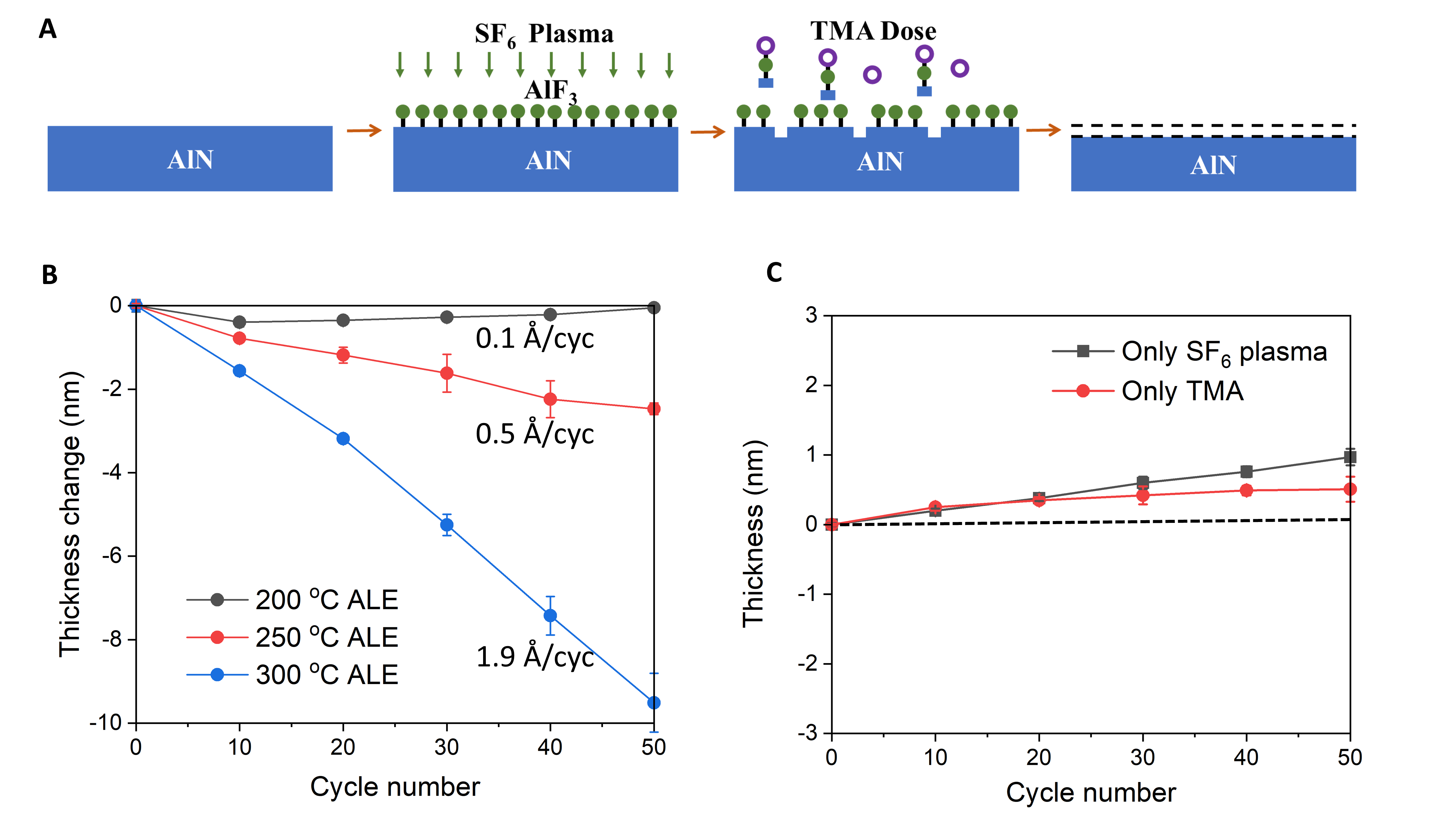
Fig. 1 shows the AlN film thickness change versus cycle number for different process temperatures with other parameters fixed. At 200 ∘C, we observe an initial etch in the first 10 cycles followed by a subsequent thickness increase, with an overall etch rate of 0.1 Å/cycle over 50 cycles. At 250 ∘C, a monotonic trend of thickness change is observed with an EPC of 0.5 Å/cycle. The maximum EPC of 1.9 Å/cycle was achieved at 300 ∘C. The EPC increase with temperature is generally consistent with prior thermal ALE studies george2020 and those using the isotropic plasma ALE approach employed here chittock2020 .
To confirm that both half-reactions are required for etching, in Fig. 1 we show the measured thickness change versus cycle number for SF6-plasma-only and TMA-only processes at 300∘C. No etching is observed with either recipe. These results support the proposed atomic layer etching mechanism requiring both half-reactions.
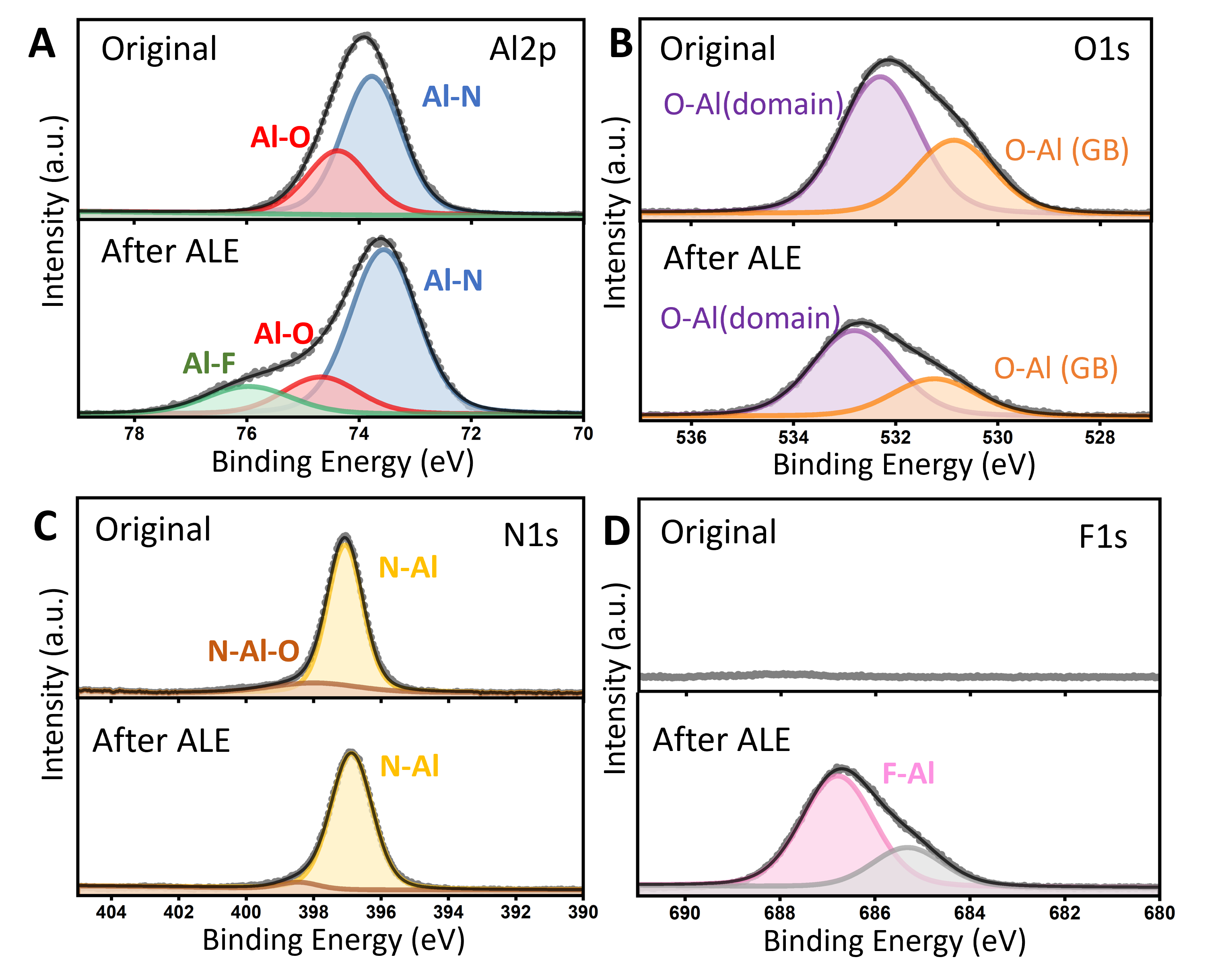
The chemical composition of original AlN thin films was characterized by XPS. In Fig. 3, the XPS core levels for the Al2p, N1s, O1s, and F1s peaks are shown. We adopt the subpeak assignment from Ref. rosenberger2008 unless specified otherwise. For the Al2p spectrum (Fig. 2) of the original AlN thin film, we observe two subpeaks at 73.7 eV and 74.4 eV, assigned to Al–N and Al–O bonds, respectively. The O1s energy profile for AlN before ALE is shown in Fig. 2, and two subpeaks separated by 1.4 eV can be identified. We assign these two subpeaks to the O-Al bond in the bulk and grain boundaries, respectively. The N1s core level spectrum (Fig. 2) has a primary N-Al subpeak at 396.8 eV and a secondary N-Al-O subpeak at 398.0 eV.
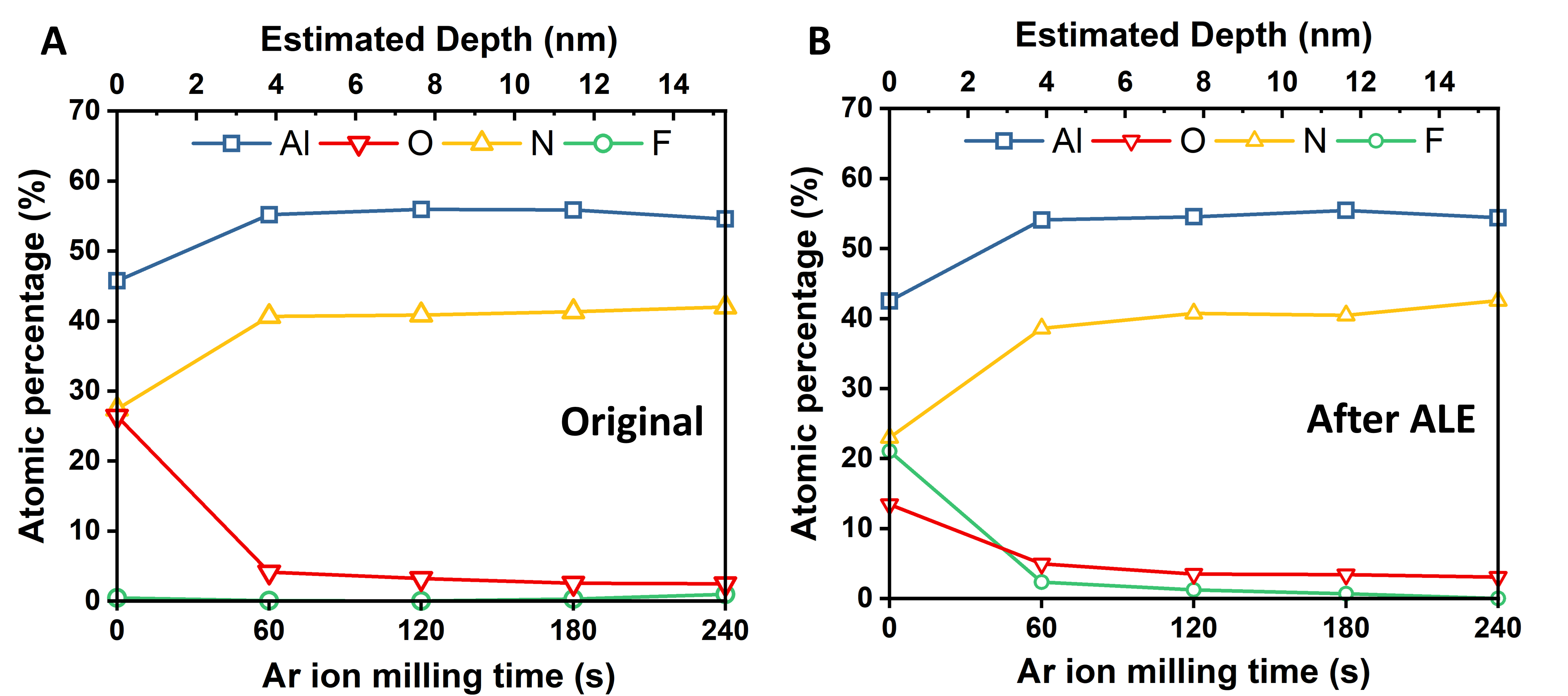
We performed XPS depth profiling to determine the atomic concentration in the surface and bulk. As shown in Fig. 3, the atomic concentrations at the surface of original AlN film are 45.7% (Al), 27.4% (N), and 26.4% (O). Below nm (after 60 s Ar ion beam exposure), the atomic concentrations plateau to their bulk values of 55.2% (Al) 40.6% (N) 4.13% (O). The higher oxygen concentration at the surface is consistent with the presence of a native oxide rosenberger2008 ; motamedi2014 .
We now examine the composition after ALE. In Fig. 2, we observe the appearance of an F1s peak after ALE, indicating the presence of residual fluorine in the surface. The F1s peak has primary subpeaks at 686.8 eV, assigned to Al-F which is consistent with prior studies on fluorinated AlN watanabe2005 . Prior work also reported an additional subpeak with weaker intensity; hennessy2016 ; moreno2018 ; fischer2017plasma this subpeak is also observed here at 685.2 eV. This subpeak lacks a known assignment. For the Al2p spectrum after ALE shown in Fig. 2, an additional subpeak at 76.0 eV is observed and assigned to the Al-F bond watanabe2005 . The O1s energy profile after ALE is shown in Fig. 2 with same O-Al subpeaks for bonds in the domain and at grain boundaries. For N1s, the position of secondary peak is shifted to 398.4 eV but the intensity is % of the total N1s intensity. To the best of our knowledge, a bond assignment for this subpeak is not available.
The XPS depth profile of the ALE-treated AlN sample is shown in Fig. 3. It is notable that the surface oxygen concentration decreased to 13.5%, indicating a lesser presence of native oxide compared to the original film. The fluorine concentration is found to be 21% at the surface. After 60 s Ar ion milling, the fluorine concentration decreases to 2% and the fractions of Al and N are within 95% of those in the original film. This observation confirms that the alteration to the chemical composition of the film from the SF6 plasma is confined to within a few nanometers of the surface, consistent with the findings of other works involving the interactions of fluorine plasmas with dielectric films fischer2017plasma .
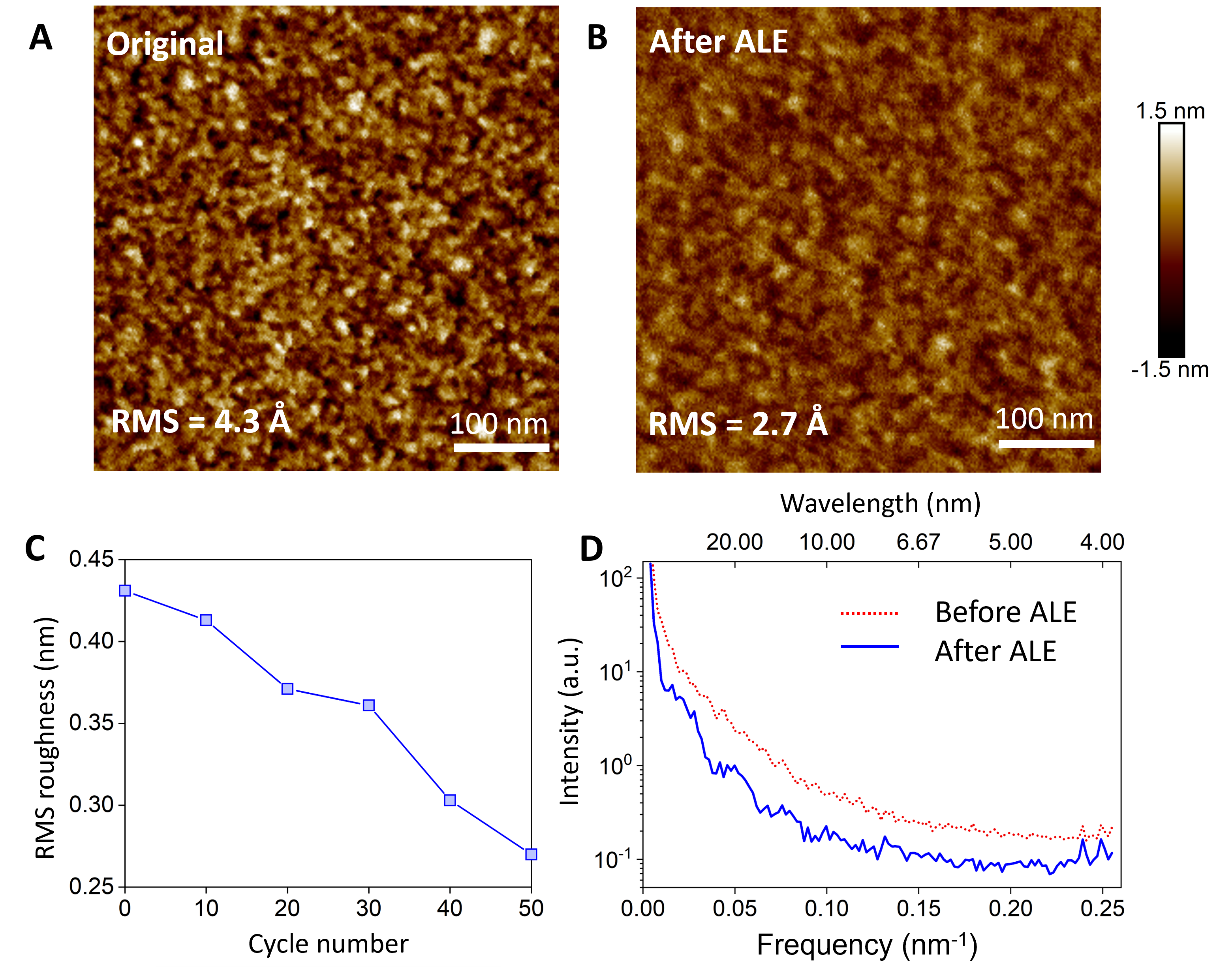
We next characterized the surface roughness of the film before and after ALE using Atomic Force Microscopy (AFM). Figs. 4 and 4 show AFM images of the film before and after ALE at 300 ∘C, respectively. Over an area of m2, the RMS roughness decreased %, from 4.3 Å to 2.7 Å, after 50 cycles of ALE. The RMS roughness versus cycle number is plotted in Fig. 4. A monotonic decrease in surface roughness is observed with cycle number. This observation was reproduced on three separate regions on each sample.
The power spectral density (PSD) of the surface was computed using the measured AFM scans. The PSD provides a quantitative measure of the lateral distance over which the surface profile varies in terms of spatial frequencies elson1995 ; myers2021 ; dash2009 ; gong2016 . The PSD was calculated by removing tilt via linear plane-fit and subsequently performing a 1D-discrete Fourier transform over each row and column in the raw AFM data. The transformed data were then averaged along one dimension to produce single PSD curve. The PSD computed from Figs. 4 and 4 are plotted in Fig. 4. A uniform decrease in roughness is observed over all spatial frequencies, indicating that both high and low spatial frequency components are smoothed by the ALE process.
We now discuss the characteristics of our isotropic plasma ALE process in context with thermal ALE processes for AlN and related materials. Thermal ALE of AlN has been reported previously using HF and Sn(acac)2 johnson2016 and HF or XeF2 and BCl3 cano2022 . The maximum EPC reported for the latter process was 0.93 Å at a substrate temperature of 300 ∘C cano2022 . Neglecting possible differences between stage and substrate temperatures, the present process achieves a nearly two-fold increase in EPC at a comparable temperature. The present process also enables similar EPCs as the thermal process at lower temperatures. Similar observations regarding higher etch rates at a given temperature using an isotropic plasma ALE process was reported in Ref. chittock2020 for etching of alumina with the same reactants. These observations offer evidence for the benefits of isotropic plasma ALE processes compared with purely thermal methods.
Our isotropic plasma ALE process may find potential applications in on-chip nonlinear and quantum photonics based on AlN, for which scattering by surface imperfections represents a primary limitation for various figures of merit. Based on the measured PSD, our process decreases surface roughness of features with periods up to tens of nanometers. This smoothing capability may enable the reduction in sidewall roughness due to reactive ion etching as well as lithographic roughness transferred from the resist to the film, which would in turn reduce optical losses.
In summary, we reported an isotropic plasma ALE process for AlN using sequential SF6 plasma and Al(CH3)3 exposures. The etch rate reaches a maximum of 1.9 Å/cycle at 300 ∘C. We observe a smoothing effect from ALE, with a decrease in RMS roughness of % after 50 cycles. The surface oxygen content is significantly decreased after ALE, indicating that native oxides are largely removed by the process. We anticipate that the ability to engineer the surface of AlN films with enhanced precision using isotropic plasma ALE will facilitate applications of AlN in nonlinear photonics and electronics.
Acknowledgements
This work was supported by Kavli Foundation and by the AFOSR under Grant Number FA9550-19-1-0321. The authors thank Nicholas Chittock, Guy DeRose, Harm Knoops, Kelly McKenzie, and Russ Renzas for useful discussions. We gratefully acknowledge the critical support and infrastructure provided for this work by The Kavli Nanoscience Institute and the Molecular Materials Research Center of the Beckman Institute at the California Institute of Technology.
References
- (1) Chi Xiong, Wolfram HP Pernice, Xiankai Sun, Carsten Schuck, King Y Fong, and Hong X Tang. Aluminum nitride as a new material for chip-scale optomechanics and nonlinear optics. New Journal of Physics, 14(9):095014, 2012.
- (2) Tsung-Ju Lu, Michael Fanto, Hyeongrak Choi, Paul Thomas, Jeffrey Steidle, Sara Mouradian, Wei Kong, Di Zhu, Hyowon Moon, Karl Berggren, , Jeehwan Kim, Mohammad Soltani, Stefan Preble, and Dirk Englund. Aluminum nitride integrated photonics platform for the ultraviolet to visible spectrum. Optics express, 26(9):11147–11160, 2018.
- (3) Bowei Dong, Xianshu Luo, Shiyang Zhu, Mo Li, Dihan Hasan, Li Zhang, Soo Jin Chua, Jingxuan Wei, Yuhua Chang, Guo-Qiang Lo, Kah Wee Ang, Dim-Lee Kwong, and Chengkuo Lee. Aluminum nitride on insulator (AlNOI) platform for mid-infrared photonics. Optics Letters, 44(1):73, jan 1, 2019. ISSN 0146-9592. URL https://www.osapublishing.org/abstract.cfm?{URI}=ol-44-1-73.
- (4) Pao Tai Lin, Hojoong Jung, Lionel C Kimerling, Anu Agarwal, and Hong X Tang. Low-loss aluminium nitride thin film for mid-infrared microphotonics. Laser & Photonics Reviews, 8(2):L23–L28, 2014.
- (5) Yoshitaka Taniyasu, Makoto Kasu, and Toshiki Makimoto. An aluminium nitride light-emitting diode with a wavelength of 210 nanometres. nature, 441(7091):325–328, 2006.
- (6) S Zhao, AT Connie, MHT Dastjerdi, XH Kong, Q Wang, M Djavid, S Sadaf, XD Liu, I Shih, H Guo, and Z Mi. Aluminum nitride nanowire light emitting diodes: Breaking the fundamental bottleneck of deep ultraviolet light sources. Scientific reports, 5(1):1–5, 2015.
- (7) Hyeong-Soon Jang, Donghwa Lee, Hyungjun Heo, Yong-Su Kim, Hyang-Tag Lim, Seung-Woo Jeon, Sung Moon, Sangin Kim, Sang-Wook Han, and Hojoong Jung. Aluminum nitride waveguide beam splitters for integrated quantum photonic circuits. arXiv preprint arXiv:2208.01377, 2022.
- (8) Noel H Wan, Tsung-Ju Lu, Kevin C Chen, Michael P Walsh, Matthew E Trusheim, Lorenzo De Santis, Eric A Bersin, Isaac B Harris, Sara L Mouradian, Ian R Christen, Isaac B. Harris, Sara L. Mouradian, Ian R. Christen, Edward S. Bielejec, and Dirk Englund. Large-scale integration of artificial atoms in hybrid photonic circuits. Nature, 583(7815):226–231, 2020.
- (9) Wolfram Hans Peter Pernice, C Xiong, C Schuck, and HX Tang. High-q aluminum nitride photonic crystal nanobeam cavities. Applied Physics Letters, 100(9):091105, 2012.
- (10) Yi Sun, Walter Shin, David Arto Laleyan, Ping Wang, Ayush Pandey, Xianhe Liu, Yuanpeng Wu, Mohammad Soltani, and Zetian Mi. Ultrahigh q microring resonators using a single-crystal aluminum-nitride-on-sapphire platform. Optics letters, 44(23):5679–5682, 2019.
- (11) Xianwen Liu, Zheng Gong, Alexander W Bruch, Joshua B Surya, Juanjuan Lu, and Hong X Tang. Aluminum nitride nanophotonics for beyond-octave soliton microcomb generation and self-referencing. Nature communications, 12(1):1–7, 2021.
- (12) Wolfram Hans Peter Pernice, C Xiong, C Schuck, and HX Tang. Second harmonic generation in phase matched aluminum nitride waveguides and micro-ring resonators. Applied Physics Letters, 100(22):223501, 2012.
- (13) Daniel D. Hickstein, Hojoong Jung, David R. Carlson, Alex Lind, Ian Coddington, Kartik Srinivasan, Gabriel G. Ycas, Daniel C. Cole, Abijith Kowligy, Connor Fredrick, Stefan Droste, Erin S. Lamb, Nathan R. Newbury, Hong X. Tang, Scott A. Diddams, and Scott B. Papp. Ultrabroadband supercontinuum generation and frequency-comb stabilization using on-chip waveguides with both cubic and quadratic nonlinearities. Phys. Rev. Applied, 8:014025, Jul 2017. URL https://link.aps.org/doi/10.1103/PhysRevApplied.8.014025.
- (14) H Oikawa, R Akiyama, K Kanazawa, S Kuroda, I Harayama, K Nagashima, D Sekiba, Y Ashizawa, A Tsukamoto, K Nakagawa, and N. Ota. Deposition and characterization of amorphous aluminum nitride thin films for a gate insulator. Thin Solid Films, 574:110–114, 2015.
- (15) Carl-Mikael Zetterling, Mikael Östling, Chris I Harris, Nils Nordell, K Wongchotigul, and Michael G Spencer. Comparison of sio2 and aln as gate dielectric for sic mos structures. In Materials Science Forum, volume 264, pages 877–880. Trans Tech Publications Inc., 1998.
- (16) Yong Ju Lee. Formation of aluminum nitride thin films as gate dielectrics on si (1 0 0). Journal of crystal growth, 266(4):568–572, 2004.
- (17) T Adam, J Kolodzey, CP Swann, MW Tsao, and JF Rabolt. The electrical properties of mis capacitors with aln gate dielectrics. Applied Surface Science, 175:428–435, 2001.
- (18) Hsiao-Wen Zan, Kuo-Hsi Yen, Chien-Hsun Chen, Pu-Kuan Liu, Kuo-Hsin Ku, and Jennchang Hwang. Organic thin-film transistors with low-temperature aln film as gate insulator. Electrochemical and solid-state letters, 10(1):H8, 2006.
- (19) MM De Souza, S Jejurikar, and KP Adhi. Impact of aluminum nitride as an insulator on the performance of zinc oxide thin film transistors. Applied Physics Letters, 92(9):093509, 2008.
- (20) C Besleaga, GE Stan, I Pintilie, P Barquinha, E Fortunato, and R Martins. Transparent field-effect transistors based on aln-gate dielectric and igzo-channel semiconductor. Applied Surface Science, 379:270–276, 2016.
- (21) D Buttari, Alessandro Chini, T Palacios, R Coffie, L Shen, H Xing, S Heikman, L McCarthy, A Chakraborty, S Keller, and U. K. Mishra. Origin of etch delay time in cl 2 dry etching of algan/gan structures. Applied physics letters, 83(23):4779–4781, 2003.
- (22) Hong Chen, Jingan Zhou, Dongying Li, Dongyu Chen, Abhinav K Vinod, Houqiang Fu, Xuanqi Huang, Tsung-Han Yang, Jossue A Montes, Kai Fu, Chen Yang, Cun-Zheng Ning, Chee Wei Wong, Andrea M. Armani, and Yuji Zhao. Supercontinuum generation in high order waveguide mode with near-visible pumping using aluminum nitride waveguides. ACS Photonics, 8(5):1344–1352, 2021.
- (23) Inna Krasnokutska, Jean-Luc J Tambasco, Xijun Li, and Alberto Peruzzo. Ultra-low loss photonic circuits in lithium niobate on insulator. Optics express, 26(2):897–904, 2018.
- (24) Keren J Kanarik, Thorsten Lill, Eric A Hudson, Saravanapriyan Sriraman, Samantha Tan, Jeffrey Marks, Vahid Vahedi, and Richard A Gottscho. Overview of atomic layer etching in the semiconductor industry. Journal of Vacuum Science & Technology A: Vacuum, Surfaces, and Films, 33(2):020802, 2015.
- (25) Steven M George. Mechanisms of thermal atomic layer etching. Accounts of Chemical Research, 53(6):1151–1160, 2020.
- (26) Xia Sang, Yantao Xia, Philippe Sautet, and Jane P Chang. Atomic layer etching of metals with anisotropy, specificity, and selectivity. Journal of Vacuum Science & Technology A: Vacuum, Surfaces, and Films, 38(4):043005, 2020.
- (27) Harm CM Knoops, Tahsin Faraz, Karsten Arts, and Wilhelmus MM Kessels. Status and prospects of plasma-assisted atomic layer deposition. Journal of Vacuum Science & Technology A: Vacuum, Surfaces, and Films, 37(3):030902, 2019.
- (28) Max N Yoder. Atomic layer etching. Technical report, DEPARTMENT OF THE NAVY WASHINGTON DC, 1988.
- (29) Hiroyuki Sakaue, Seiji Iseda, Kazushi Asami, Jirou Yamamoto, Masataka Hirose, and Yasuhiro Horiike. Atomic layer controlled digital etching of silicon. Japanese journal of applied physics, 29(11R):2648, 1990.
- (30) Y Horiike, T Tanaka, M Nakano, S Iseda, H Sakaue, A Nagata, H Shindo, S Miyazaki, and M Hirose. Digital chemical vapor deposition and etching technologies for semiconductor processing. Journal of Vacuum Science & Technology A: Vacuum, Surfaces, and Films, 8(3):1844–1850, 1990.
- (31) Younghee Lee, Craig Huffman, and Steven M George. Selectivity in thermal atomic layer etching using sequential, self-limiting fluorination and ligand-exchange reactions. Chemistry of Materials, 28(21):7657–7665, 2016.
- (32) Jaime W DuMont and Steven M George. Competition between al2o3 atomic layer etching and alf3 atomic layer deposition using sequential exposures of trimethylaluminum and hydrogen fluoride. The Journal of Chemical Physics, 146(5):052819, 2017.
- (33) John Hennessy, Christopher S Moore, Kunjithapatham Balasubramanian, April D Jewell, Kevin France, and Shouleh Nikzad. Enhanced atomic layer etching of native aluminum oxide for ultraviolet optical applications. Journal of Vacuum Science & Technology A: Vacuum, Surfaces, and Films, 35(4):041512, 2017.
- (34) David R Zywotko, Jacques Faguet, and Steven M George. Rapid atomic layer etching of al2o3 using sequential exposures of hydrogen fluoride and trimethylaluminum with no purging. Journal of Vacuum Science & Technology A: Vacuum, Surfaces, and Films, 36(6):061508, 2018.
- (35) Austin M Cano, Amy E Marquardt, Jaime W DuMont, and Steven M George. Effect of hf pressure on thermal al2o3 atomic layer etch rates and al2o3 fluorination. The Journal of Physical Chemistry C, 123(16):10346–10355, 2019.
- (36) Nicholas J Chittock, Martijn FJ Vos, Tahsin Faraz, Wilhelmus MM Kessels, Harm CM Knoops, and Adriaan JM Mackus. Isotropic plasma atomic layer etching of al2o3 using a fluorine containing plasma and al (ch3) 3. Applied Physics Letters, 117(16):162107, 2020.
- (37) Rezwanur Rahman, Eric C Mattson, Joseph P Klesko, Aaron Dangerfield, Sandrine Rivillon-Amy, David C Smith, Dennis Hausmann, and Yves J Chabal. Thermal atomic layer etching of silica and alumina thin films using trimethylaluminum with hydrogen fluoride or fluoroform. ACS applied materials & interfaces, 10(37):31784–31794, 2018.
- (38) Jaime W DuMont, Amy E Marquardt, Austin M Cano, and Steven M George. Thermal atomic layer etching of sio2 by a “conversion-etch” mechanism using sequential reactions of trimethylaluminum and hydrogen fluoride. ACS applied materials & interfaces, 9(11):10296–10307, 2017.
- (39) Wenjie Lu, Younghee Lee, Jonas C Gertsch, Jessica A Murdzek, Andrew S Cavanagh, Lisa Kong, Jesús A Del Alamo, and Steven M George. In situ thermal atomic layer etching for sub-5 nm ingaas multigate mosfets. Nano letters, 19(8):5159–5166, 2019.
- (40) Andreas Fischer, Aaron Routzahn, Steven M George, and Thorsten Lill. Thermal atomic layer etching: A review. Journal of Vacuum Science & Technology A: Vacuum, Surfaces, and Films, 39(3):030801, 2021.
- (41) Chang Fang, Yanqiang Cao, Di Wu, and Aidong Li. Thermal atomic layer etching: Mechanism, materials and prospects. Progress in Natural Science: Materials International, 28(6):667–675, 2018.
- (42) Younghee Lee, Jaime W DuMont, and Steven M George. Atomic layer etching of hfo2 using sequential, self-limiting thermal reactions with sn (acac) 2 and hf. ECS Journal of Solid State Science and Technology, 4(6):N5013, 2015.
- (43) Keren J. Kanarik, Samantha Tan, Wenbing Yang, Taeseung Kim, Thorsten Lill, Alexander Kabansky, Eric A. Hudson, Tomihito Ohba, Kazuo Nojiri, Jengyi Yu, Rich Wise, Ivan L. Berry, Yang Pan, Jeffrey Marks, and Richard A. Gottscho. Predicting synergy in atomic layer etching. Journal of Vacuum Science & Technology A: Vacuum, Surfaces, and Films, 35(5):05C302, sep 2017. ISSN 0734-2101. URL http://avs.scitation.org/doi/10.1116/1.4979019.
- (44) Tomihito Ohba, Wenbing Yang, Samantha Tan, Keren J Kanarik, and Kazuo Nojiri. Atomic layer etching of gan and algan using directional plasma-enhanced approach. Japanese Journal of Applied Physics, 56(6S2):06HB06, 2017.
- (45) Nicholas R Johnson, Huaxing Sun, Kashish Sharma, and Steven M George. Thermal atomic layer etching of crystalline aluminum nitride using sequential, self-limiting hydrogen fluoride and sn (acac) 2 reactions and enhancement by h2 and ar plasmas. Journal of Vacuum Science & Technology A: Vacuum, Surfaces, and Films, 34(5):050603, 2016.
- (46) Austin M Cano, Ann Lii-Rosales, and Steven M George. Thermal atomic layer etching of aluminum nitride using hf or xef2 for fluorination and bcl3 for ligand exchange. The Journal of Physical Chemistry C, 126(16):6990–6999, 2022.
- (47) Joel W Clancey, Andrew S Cavanagh, James ET Smith, Sandeep Sharma, and Steven M George. Volatile etch species produced during thermal al2o3 atomic layer etching. The Journal of Physical Chemistry C, 124(1):287–299, 2019.
- (48) Leland Rosenberger, Ronald Baird, Erik McCullen, Gregory Auner, and Gina Shreve. Xps analysis of aluminum nitride films deposited by plasma source molecular beam epitaxy. Surface and Interface Analysis: An International Journal devoted to the development and application of techniques for the analysis of surfaces, interfaces and thin films, 40(9):1254–1261, 2008.
- (49) Pouyan Motamedi and Ken Cadien. Xps analysis of aln thin films deposited by plasma enhanced atomic layer deposition. Applied Surface Science, 315:104–109, 2014.
- (50) Morimichi Watanabe, Yukimasa Mori, Takahiro Ishikawa, Hiroaki Sakai, Takashi Iida, Keijiro Akiyama, Shogo Narita, Kyoichi Sawabe, and Kosuke Shobatake. Thermal reaction of polycrystalline aln with xe f 2. Journal of Vacuum Science & Technology A: Vacuum, Surfaces, and Films, 23(6):1647–1656, 2005.
- (51) John Hennessy, April D Jewell, Kunjithapatham Balasubramanian, and Shouleh Nikzad. Ultraviolet optical properties of aluminum fluoride thin films deposited by atomic layer deposition. Journal of Vacuum Science & Technology A: Vacuum, Surfaces, and Films, 34(1):01A120, 2016.
- (52) Juan C Moreno-López, Gustavo Ruano, Julio Ferrón, Paola Ayala, and Mario CG Passeggi Jr. Thermally annealed sub-monolayers of alf3 on cu (100): An stm and xps study. physica status solidi (b), 255(12):1800389, 2018.
- (53) Andreas Fischer, Richard Janek, John Boniface, Thorsten Lill, KJ Kanarik, Yang Pan, Vahid Vahedi, and Richard A Gottscho. Plasma-assisted thermal atomic layer etching of al2o3. In Advanced Etch Technology for Nanopatterning VI, volume 10149, pages 20–24. SPIE, 2017.
- (54) J Merle Elson and Jean M Bennett. Calculation of the power spectral density from surface profile data. Applied optics, 34(1):201–208, 1995.
- (55) Tyler J Myers, James A Throckmorton, Rebecca A Borrelli, Malcolm O’Sullivan, Tukaram Hatwar, and Steven M George. Smoothing surface roughness using al2o3 atomic layer deposition. Applied Surface Science, 569:150878, 2021.
- (56) P Dash, P Mallick, H Rath, A Tripathi, Jai Prakash, DK Avasthi, S Mazumder, S Varma, PV Satyam, and NC Mishra. Surface roughness and power spectral density study of shi irradiated ultra-thin gold films. Applied Surface Science, 256(2):558–561, 2009.
- (57) Yuxuan Gong, Scott T Misture, Peng Gao, and Nathan P Mellott. Surface roughness measurements using power spectrum density analysis with enhanced spatial correlation length. The Journal of Physical Chemistry C, 120(39):22358–22364, 2016.