Localized creation of yellow single photon emitting carbon complexes in hexagonal boron nitride
Abstract
Single photon emitters in solid-state crystals have received a lot of attention as building blocks for numerous quantum technology applications. Fluorescent defects in hexagonal boron nitride (hBN) stand out due to their high luminosity and robust operation at room temperature. The fabrication of identical emitters at pre-defined sites is still challenging, which hampers the integration of these defects in optical systems and electro-optical devices. Here, we demonstrate the localized fabrication of hBN emitter arrays by electron beam irradiation using a standard scanning electron microscope with deep sub-micron lateral precision. The emitters are created with a high yield and a reproducible spectrum peaking at 575 nm. Our measurements of optically detected magnetic resonance have not revealed any addressable spin states. Using density functional theory, we attribute the experimentally observed emission lines to carbon-related defects, which are activated by the electron beam. Our scalable approach provides a promising pathway for fabricating room temperature single photon emitters in integrated quantum devices.
I Introduction
Many quantum photonic technologies, such as optical quantum computing and quantum communication, require sources of true single photons [1, 2, 3, 4, 5, 6]. The generation of ideal single photons on demand, however, still remains a technical challenge. Due to their in principle simple operation requirements and possibilities for integration, solid-state color centers are promising candidates for single photon sources as opposed to semiconductor quantum dots. While the latter can emit simultaneously pure and indistinguishable single photons [7], the need for cryogenic cooling below 4 K prevents using quantum dots in broad applications. Within the class of solid-state single photon emitters (SPEs) [8], color centers hosted by two-dimensional (2D) materials have the advantage of featuring an in-plane dipole that emits out-of-plane (in case of intra-layer defects) [9, 10, 11]. This simplifies the extraction and collection of the generated single photons, together with the fact that in atomically thin materials the emitters are not surrounded by any high refractive index material and are thus not affected by total internal or Fresnel reflection.
Single photon emitters hosted by 2D crystals have been observed initially in semiconducting transition metal dichalcogenides (TMDs) [12, 13, 14, 15, 16, 17, 18] and in insulating hexagonal boron nitride (hBN) [19]. The wide bandgap of hBN allows for the formation of deep defect-induced energy levels that are well-isolated from the band edges. This in turn leads to a high quantum efficiency at room temperature [20] and is one of the reasons for the high single photon luminosity. Also contributing to this is a short excited-state lifetime [21] and the aforementioned high extraction efficiency. Unlike the nitrogen vacancy center in diamond, hBN emitters in the visible spectrum often have a strong coupling into the zero-phonon line (ZPL) with only weak phonon coupling that leads to coherent emission [22].
The quantum emitters in hBN can be fabricated in a rich variety of ways: thermal activation of naturally occurring emitters [19], plasma and chemical etching [21, 23], nanoindentation with an atomic force microscope (AFM) [24], strain-activation through transfer [25] or growth on pillared substrates [26], laser or gamma-ray damage [27, 28], and irradiation with electrons or ions [29, 30, 31, 32, 33]. While the strain activation localizes the emitter by default, many of the other fabrication techniques cause the emitter to form at random locations. Radiation damage has the potential for localization as well, since a laser or a charged particle beam can be easily focused onto a spot. The diffraction limit of electrons and ions is dependent on the particle energy and is typically on the order of a few nm, which may allow one to fabricate emitters with extremely high accuracy.
In order to build integrated quantum devices with a scalable fabrication process, this precise control over the emitter location is crucial. Moreover, depending on the application, spectral control is also important. Quantum emitters have been experimentally reported with emission wavelengths in the UV [34], the entire visible spectrum [35], and in the NIR [36]. Potentially, this can be extended to telecom wavelengths [37]. In addition, theoretical simulations have shown that hBN emitters cover important wavelengths for quantum technologies [38]. Spectral control is difficult to achieve because the nature and type of these defects is still a topic of ongoing research. Recent studies supported by density functional theory (DFT) calculations have identified carbon- and oxygen-related defects, as well as the negatively charged boron vacancy [39, 40, 41, 42, 43].
In this work, we address both issues of position and spectral control in the fabrication of quantum emitters in hBN. Using localized electron irradiation in a scanning electron microscope (SEM), we realize localized quantum emitters with a high yield. The high lateral resolution of the SEM allows us to restrict the emitter formation with sub-micron precision at pre-defined spots. While previous studies have found this to work reliably for blue emitters [30, 31], our method expands this to yellow emitters with a reproducible wavelength and also does not require high temperature annealing (similar to other emitters fabricated by electron irradiation). We have also investigated the defects for addressable spin states through optically detected magnetic resonance (ODMR) [44, 45, 46]. Together with DFT calculations, we propose a possible atomic structure of the defect complex with a ZPL close to the yellow emitters.
II Methods
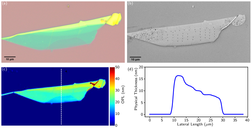
An hBN flake is mechanically exfoliated from a bulk crystal using scotch tape onto a PDMS (polydimethylsiloxane) stamp. Thin flakes (typically in the range of 5 nm to 20 nm) are selected based on the optical contrast in a bright field microscope and transferred to a grid-patterned Si/SiO2 substrate (see Supplementary Section S1). Figures 1(a) and (b) show an optical and SEM image, respectively, of a typical exfoliated hBN flake. The precise flake thickness is measured using a phase-shift interferometer (PSI), which measures the optical path length (OPL) through the flake and converts this using RCWA (rigorous coupled-wave analysis) simulations to the physical thickness. This technique was found to be highly accurate for 2D materials, yet is much faster than the commonly used AFMs [21, 9]. An OPL map is shown in Figure 1(c), with the physical thickness along the dashed line shown in Figure 1(d).
The quantum emitters are created by irradiating the hBN flake with an electron beam using a scanning electron microscope without any pre-treatment. The high lateral resolution of the SEM allows us to restrict the interaction of the electrons with the hBN to small volumes, thereby localizing the emitter formation at any arbitrarily chosen spots with sub-micron precision. The number of emitters created depends on the fabrication parameters. For all experiments, we used an acceleration voltage of 3 kV and an electron current of 25 pA in the field-free operation mode of the SEM. The theoretical resolution limit of our SEM is 2.8 nm, however, with the used beam alignment we estimate the beam diameter to be around 300 nm. Since this is already the diffraction limit for the subsequent optical characterization, we did not optimize this any further. The analysis of the irradiated spot size is summarized in the Supplementary Section S2. The dose is controlled by the irradiation time and we found an optimal dwell times of 10 s, which results in a particle fluence of cm-2. Pointing the electron beam to a single point produces single spots as is evident from the SEM image (see Figure 1(b)), however, higher doses allow us to directly write emitter ensembles and larger patterns (see Supplementary Section S1). We note that the fluence values used to record the SEM images ( cm-2) are low compared to the conditions for emitter writing to avoid accidental fabrication of emitters.
It is known from the literature that many fabrication techniques require post-processing, in particular thermal annealing which either activates the emitter or at least enhances the intensity [35, 31, 47]. To investigate the impact of annealing on the emission properties (which are studied in detail in the next section), a flake is prepared with an emitter array of irradiated spots. Our photoluminescence (PL) map reveal that the emitter array that is present initially disappears after treatment with typical annealing conditions in a furnace at 850 ∘C under an inert argon atmosphere (600 mbar pressure) for 30 min (see Supplementary Section S3). We found that this annealing can activate other (uncorrelated) contaminants, but also heals ours through the SEM activated or created emitters. This suggests a high mobility and subsequent instability of the involved defects at such high temperatures. As a consequence, we conclude there is no post-processing necessary after the SEM treatment, which simplifies the fabrication. Other experiments on electron-irradiated hBN emitters have confirmed this [33, 30]. We note that Gale et al. reported that pre-annealing can enhance cathodoluminescence at 305 nm, which reveals the presence of the CC dimer that can be correlated to the blue emitter [31].
The emitter fabrication with an electron beam is influenced by the electron beam diameter and electron scattering in the hBN lattice. To further study this interaction, an electron dose-dependent irradiation is performed by varying the electron irradiation time. An array of emitters is fabricated where each spot is irradiated for a different irradiation time. The photon count rate at the irradiated spot presents the saturation behaviour as a function of irradiation time. This indicates the creation/activation of the emitter is bounded to the maximum emitter density [48]. The optical characterization (for the details see the following section) and analysis are summarized in Supplementary Section S4. However, the emission from individual emitters in an ensemble is uncorrelated and therefore, these sites are not emitting single photons anymore. The probability of forming a single isolated emitter decreases with increasing the electron fluence, while at the same time, the probability of multiple emitters increases. This suggests that the emitter’s formation could be governed by Poisson statistics. Thus producing single emitters with a high yield requires a careful calibration of electron fluence.
III Results
III.1 Optical characterization
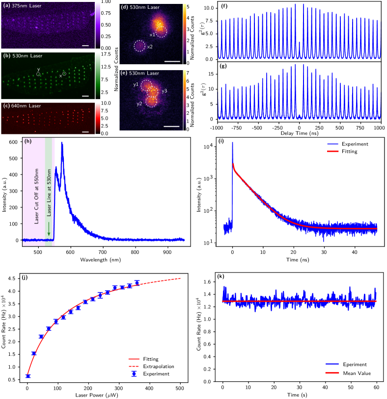
To identify if the fabrication parameters are feasible, we have optically characterized the created emitters with a commercial fluorescence lifetime imaging microscope (see Supplementary Section S5). All measurements have been performed at room temperature and with an excitation laser pulse with repetition rate of 20 MHz. Our setup allows us to use different laser heads with fixed wavelengths of 375 nm, 530 nm, and 640 nm and pulse lengths in the range below 40 ps to 90 ps. The PL images for the different excitation energies are shown in Figures 2(a-c). As the crystal is always excited below the bandgap, there is bright emission at electron-irradiated spots only. The brightness, however, strongly depends on the excitation energy. Note that the color scale for each PL map has been normalized such that the brightest emitter in Figure 2(a) under excitation with 375 nm laser light has a PL intensity of 1 a.u. As can be seen, the excitation is very inefficient in the UV, in particular, the blue emitters at 435 nm were not present. This suggests that our sample does not contain the CC dimer that can be correlated to the blue emitter [31]. In contrast to the UV excitation, the emitters are the brightest under the illumination of 530 nm excitation laser. We would like to mention that we have dynamically adapted the spacing between the irradiation spots so that our array does not have periodic spacing. This was due to the fact that the mechanically exfoliated flakes typically have random shapes and we did not want to fabricate emitters close to the crystal edges. The mean distance between irradiation spots is roughly 3 m. In the overlayed SEM and PL image (see Supplementary Section S6), it becomes clear that all irradiated spots have a corresponding bright spot in the PL image. The number of emitters per irradiated spot varies: while most of the time there is exactly one emitter present, sometimes there is a second emitter nearby (see Figure 2(d)) or emitter ensembles are created in the same spot (see Figure 2(e) and Supplementary Section S7). This is due to the Poisson statistics of the irradiation process. It is also worth mentioning that the bright emission from the irradiated spot is independent of the flake thickness, as shown in the overlayed OPL and PL maps (see Supplementary section S8). This could be due to the fact that the localized electron irradiation depositing carbon atoms which are responsible for the defect formation in the top layer of the hBN.
The second-order correlation function of these emitters reveals the presence of single photon emitters with the zero-delay peak under pulsed excitation dropping to 0.36 and 0.22 (without any background correction) in Figure 2(f) and (g), respectively. A value below 0.5 proves a non-zero overlap with the single photon Fock state [49] and is therefore a commonly-used criterion for single photon emission. We note that only proves rigorously single photon emission, which can be reached when the experimental imperfections are considered [50]. The details about our calculations can be found in Supplementary Section S9. The spectrally-resolved measurement of the emission reveals a peak at 575 nm when the emitter is excited with a 530 nm laser (see Figure 2(h)).
It is worth noting that our long-pass filter has a cut-off wavelength of 550 nm to suppress the excitation laser at 530 nm which partially suppresses the detection of the emission. We therefore do not have access to the full spectral information about the emitter under 530 nm excitation laser. However, to investigate the possibility of any strong peak emission in the spectrally blocked region below 550 nm, we also used a 470 nm excitation laser to excite the emitters. A long pass filter with a cut-off wavelength at 500 nm is used to collect the spectrum. We do not observe any strong emission when exciting with 470 nm laser, which excludes the possibility of any other emission peak in the blocked spectral region. Moreover, with this excitation laser we also do not observe the 575 nm peak as observed with the 530 nm excitation laser. This could be due to the fact that the 470 nm excitation laser has negligible overlap with the emitter phonon side bands (absorption) of the emitters. This can be estimated by mirroring the spectra around the peak at 575 nm (see Supplementary Section S10). The PL of the emitters under 375 nm excitation was too weak to record a spectrum above the noise floor (confirming inefficient excitation), and under 640 nm excitation, the emitters showed a rather broadband spectrum (probably dominated by phonon coupling).
In addition, the peak at 575 nm is near the Raman peak of hBN (the Raman shift of hBN [19] at 1360 cm-1 results in a peak at 571 nm). To determine if the 575 nm peak is the Raman peak we have also measured the temporally-resolved PL as shown in Figure 2(i). A fit (taking into account the instrument response function) reveals an excited state lifetime of 3.83(1) ns, consistent with other reports of hBN quantum emitters [8, 21, 51]. The spectrally-resolved measurement of the lifetime and function have shown to be independent of the wavelength. We estimated that the 575 nm peak contributes too much to the spectrum to originate from Raman scattering (because this would change the photon statistics and emitter lifetime).
The single photon intensity as a function of the laser excitation power reveals the typical saturation curve of a two-level system (see Figure 2(j)) and a fit with
| (1) |
allows us to extract a saturation power of W and a maximum photon count rate of kHz. The dark count rate has a negligible effect on the fit due to the low dark count rate of our single photon detectors. The detected maximum photon count rate, however, is not the actual maximum emission rate because it is limited by the collection, transmission, and detection efficiencies. The former can be addressed by coupling the emitter with resonant cavities [51] that shape the emission to be more directional. Interestingly, we have not observed any blinking or bleaching of any of the emitters as shown by our time trace of an emitter in Figure 2(k). While this problem is known for many hBN emitters [52, 53], our electron irradiation seems to produce emitters that are not affected by this.
We have also investigated the defects for addressable spin states through optically detected magnetic resonance [44, 45, 46]. Our preliminary measurements show no signature of ODMR in the typical bandwidth ranging from 3 GHz to 4 GHz as presented in Supplementary Section S11. However, our present measurements do not exclude the possibility of ODMR signature beyond the mentioned bandwidth, as recent work show the OMDR at 0.7 GHz reported by Stern et al. [45] and at 2.5 GHz reported by Mu et al. [54]. Our measurements are carried out on an ensemble of hBN emitters at room temperature. A control measurement with NV centers in diamond, however, demonstrated a significant ODMR contrast of that spin system and thereby, verifying the general functionality of our ODMR setup.
III.2 Statistical analysis
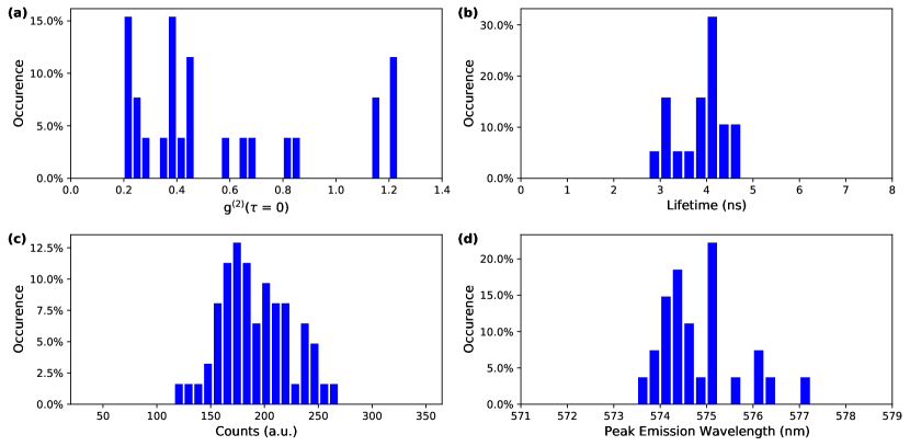
To understand if our process also produces high-quality emitters in general, we have analyzed the statistics over a larger data set containing 63 emitters fabricated on the same flake. We have decided to only include emitters hosted on the same flake in this analysis to remove the influence of the host crystal (e.g. through local strain) on the emitter properties. Figure 3(a) shows the distribution of the values, which reveals that most of the emitters can be classified as singles, while a few have and are likely ensembles. The PL maps of a subset of these emitters are presented in Supplementary Section S7.
The histogram of the lifetimes (see Figure 3(b)) reveals a mean lifetime of 3.8(5) ns (only counting emitters with ). The consistency of the lifetime provides further evidence that the emitters produced are always the same without any additional decay channels for the excited state. We note that we extracted the lifetime for the histogram from the pulsed measurement of the second-order correlation function (see Supplementary Section S12). In the limit of zero excitation power, this method would yield the correct lifetime. In our case we used this method to reduce the measurement time, as we can measure lifetime and second-order correlation time simultaneously.
The statistical distribution of the emitter brightness is presented in Figure 3(c), extracted from the PL map. For all 63 emitters presented in Figure 2(a), we wrote an automated algorithm that detects the emitter position and integrates over a diffraction-limited spot around its center (marked by the red boxes in Supplementary Section S13).
We also measure the spectrum from various other emitters exhibiting a dip in the second-order correlation measurements. We performed Gaussian fitting to extract the peak emission wavelength, which is bunching around 574.8 nm as shown in the Figure. 3(d). The mean FWHM of the peak emission wavelength is around 19.56 nm with the standard deviation of 4.44 nm (See Supplementary Section S14). This also confirms the spectral re-producibility of our fabrication method.
Emitter modeling with density functional theory
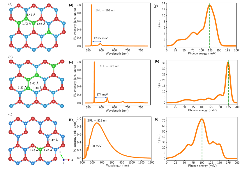
To trace back possible defect candidates that could be responsible for the yellow emission, we carried out theoretical studies using density functional theory with the HSE06 functional implemented in Vienna Ab initio Simulation Package (VASP) [55, 56] (see details in Supplementary Section S15). It is known that carbon contaminants are bonded to the surface during SEM imaging, which causes the typical dark frames. This suggests that carbon might be involved in the defect, as other calculations and experiments have demonstrated already [43, 42, 39, 38, 57, 58]. Since the experimental spectrum as shown in Figure 2(h) is a characteristic signature of all defects, we calculated the PL lineshape by employing the SCF method to determine the spectra of neutral and singly charged carbon complexes listed in Supplementary Section S15.
Our simulations identify the CCCC and CV complexes with the structural configurations depicted in Figure 4(a-c) as potential candidates for carbon-related emitters with a transition energy (i.e. ZPL) in the yellow region. In addition to the ZPL, we also calculated the phonon sideband (PSB) to obtain the complete PL spectrum (see Figure 4(d-f)). The peaks can be identified by considering the spectral function of the electron-phonon coupling or Huang-Rhys (HR) factor as shown in Figure 4(g-i). The PSB peaks in the range of 100 meV to 175 meV, which is the typical range for hBN quantum emitters. Notably, the PL spectra of the CV defect exhibits a broad peak at 380 meV from the ZPL in the calculated PL spectrum. This phenomenon can be justified by the fact that these modes have a higher energy ( meV) than the zone-center longitudinal optical phonon mode (LO()) [59]. As coupling to electrons scales with the inverse of the phonon wave vector from the Fröhlich interaction, the electron-phonon matrix element will subsequently diverge due to the singularity at this point and lead to broad PL. Based on the HR factor, the assignment of the ZPL becomes evident. To identify the contributions to the ZPL, the HR factor yielded small values of 1.033, 1.372 and 4.795, corresponding to the configuration coordinates between ground and excited states shifted by 0.456 amu1/2Å, 0.435 amu1/2Å, and 0.994 amu1/2Å, respectively, for the defect complexes shown in Figure 4(a-c). This reveals that the defects inherently emit at their assigned ZPL with only a weak contribution from phonon coupling in case of the CCCC configurations and with strong phonon coupling for the CV defect. This DFT calculation consequently proposes that CCCC is one of the potential candidates responsible for this range of emission, whereas CV is unlikely due to the mismatch of the PSB with the experiment.
Moreover, when comparing among singlet, doublet, and triplet spin configurations of CCCC, it favors the singlet configuration, implying the absence of a meta-stable triplet state. CCCC is therefore unlikely to exhibit any ODMR signature, consistent with the experimental result. Our DFT calculations achieved to narrow down the possible defect candidates with ZPL relevant to the yellow region, however, we note that the broad emission observed in the experiment still requires further analysis, which is beyond the scope of this work.
We finally answer the question of the formation mechanism. Electrons with an energy of 3 keV do not have enough momentum for knock-on damage and to displace atoms. It is likely that the electrons can bond carbon to the hBN (which causes the black spots in the SEM image) and then break these bonds and re-organize them to form the carbon complexes. Another possibility is the change of the charge state of already present defects or the enabling of a single photon emission mechanism based on donor-acceptor pairs [60].
IV Conclusions
We have demonstrated the localized fabrication of SPEs in exfoliated multilayers of hBN using focused electron beam irradiation with a well-defined set of emission properties and a high yield. Our process does not require any pre- or post-processing (e.g. thermal annealing) of the hBN crystals. All fabricated color centers emit consistently at 575 nm (2.16 eV). This has not been observed in previous work fabricating emitters with reproducible blue emission using similar electron irradiation [33, 30]. We believe that this could be due to our sample not containing the carbon dimer CC that was linked to this emission [31]. We speculate that the origin of our emitter is due to the deposition of carbon by the electron beam irradiation, the breaking and re-organization of chemical bonds, the change of the charge state of existing defects (i.e., activating them optically), or the enabling of single photon emission based on donor-acceptor pairs.[60]. This does not, however, provide an explanation why previous other works have not observed our yellow emitters. For a better overview of this work, we also provide a table comparing the recent development of 2D materials based single photon emitters in Supplementary Section S16.
Our ODMR measurements have not revealed any addressable spin states. The theoretical analysis using DFT calculations allows us to propose possible atomic structures, namely of the carbon complex CCCC. The process is reproducible and repeatable and thus allows us to fabricate identical SPEs on demand and with deep sub-micron placement accuracy. Furthermore, our study also opens up a new way to understand the nature and photophysical properties of the defect-based emitters in hBN. As the method is scalable and compatible with coupling to nanophotonics, we expect use in near-future quantum technology applications. It was recently pointed out that hBN emitters have naturally spectral overlap with many important wavelengths for quantum technologies [38]. When enhanced with resonators that reduce the linewidth [51], the yellow emitters presented here could be used to couple to other solid-state quantum systems in quantum networks such as to the PbV- color center in diamond with its ZPL at 552 nm or to the sodium D transitions at 589 nm in alkali vapor-based quantum memories [38]. Such usage, however, is only possible if the quantum emitters can be fabricated in a here demonstrated reproducible fashion.
Supplementary Material
Supplementary Material is available for this manuscript.
Conflict of Interest
The authors have no conflicts to disclose.
Author contributions
A.K. and M.M. prepared the samples. A.K. performed the irradiation. A.K. and T.M. carried out the optical characterization. C.C. and S.S. performed the DFT calculations. A.Z. carried out the ODMR experiments. A.K. and C.C. analyzed the data. F.E., S.S., and T.V. supervised the work. T.V. conceived the project.
Acknowledgements.
This work was funded by the Deutsche Forschungsgemeinschaft (DFG, German Research Foundation) - Projektnummer 445275953. The authors acknowledge support by the German Space Agency DLR with funds provided by the Federal Ministry for Economic Affairs and and Climate Action BMWK under grant number 50WM2165 (QUICK3). T.V. and F.E. are funded by the Federal Ministry of Education and Research (BMBF) under grant number 13N16292 and 13XP5053A, respectively. The major instrumentation used in this work was funded by the Free State of Thuringia via the projects 2015 FOR 0005 (ACP-FIB) and 2017 IZN 0012 (InQuoSens). C.C. acknowledges a Development and Promotion of Science and Technology Talents Project (DPST) scholarship by the Royal Thai Government. S.S. acknowledges financial support from the NSRF via the Program Management Unit for Human Resources & Institutional Development, Research and Innovation (grant number B05F650024). The computational experiments were supported by resources of the Friedrich Schiller University Jena supported in part by DFG grants INST 275/334-1 FUGG and INST 275/363-1 FUGG. We thank Jeetendra Gour for the fabrication of the cross grid patterned substrate and acknowledge fruitful discussions with Igor Aharonovich on the potential assignment of the Raman peak.Data sharing policy
The data that support the findings of this study are available from the corresponding author upon reasonable request.
References
- O’Brien, Furusawa, and Vučković [2009] J. L. O’Brien, A. Furusawa, and J. Vučković, “Photonic quantum technologies,” Nat. Photon. 3, 687–695 (2009).
- Mukai and Hatano [2020] K. Mukai and N. Hatano, “Discrete-time quantum walk on complex networks for community detection,” Phys. Rev. Res. 2, 023378 (2020).
- Aspuru-Guzik and Walther [2012] A. Aspuru-Guzik and P. Walther, “Photonic quantum simulators,” Nat. Phys. 8, 285–291 (2012).
- Cai et al. [2013] J. Cai, A. Retzker, F. Jelezko, and M. B. Plenio, “A large-scale quantum simulator on a diamond surface at room temperature,” Nat. Phys. 9, 168–173 (2013).
- Lvovsky, Sanders, and Tittel [2009] A. I. Lvovsky, B. C. Sanders, and W. Tittel, “Optical quantum memory,” Nat. Photon. 3, 706–714 (2009).
- Lo, Curty, and Tamaki [2014] H.-K. Lo, M. Curty, and K. Tamaki, “Secure quantum key distribution,” Nat. Photon. 8, 595–604 (2014).
- Senellart, Solomon, and White [2017] P. Senellart, G. Solomon, and A. White, “High-performance semiconductor quantum-dot single-photon sources,” Nat. Nanotechnol. 12, 1026–1039 (2017).
- Aharonovich, Englund, and Toth [2016] I. Aharonovich, D. Englund, and M. Toth, “Solid-state single-photon emitters,” Nat. Photon. 10, 631–641 (2016).
- Vogl et al. [2019a] T. Vogl, M. W. Doherty, B. C. Buchler, Y. Lu, and P. K. Lam, “Atomic localization of quantum emitters in multilayer hexagonal boron nitride,” Nanoscale 11, 14362–14371 (2019a).
- Hoese et al. [2020] M. Hoese, P. Reddy, A. Dietrich, M. K. Koch, K. G. Fehler, M. W. Doherty, and A. Kubanek, “Mechanical decoupling of quantum emitters in hexagonal boron nitride from low-energy phonon modes,” Sci. Adv. 6, eaba6038 (2020).
- Hoese et al. [2022] M. Hoese, M. K. Koch, F. Breuning, N. Lettner, K. G. Fehler, and A. Kubanek, “Single photon randomness originating from the symmetric dipole emission pattern of quantum emitters,” Appl. Phys. Lett. 120, 044001 (2022).
- Klein et al. [2019] J. Klein, M. Lorke, M. Florian, F. Sigger, L. Sigl, S. Rey, J. Wierzbowski, J. Cerne, K. Müller, E. Mitterreiter, and et al., “Site-selectively generated photon emitters in monolayer MoS2 via local helium ion irradiation,” Nat. Commun. 10, 2755 (2019).
- Klein et al. [2021] J. Klein, L. Sigl, S. Gyger, K. Barthelmi, M. Florian, S. Rey, T. Taniguchi, K. Watanabe, F. Jahnke, C. Kastl, and et al., “Engineering the luminescence and generation of individual defect emitters in atomically thin mos2,” ACS Photonics 8, 669–677 (2021).
- Srivastava et al. [2015] A. Srivastava, M. Sidler, A. V. Allain, D. S. Lembke, A. Kis, and A. Imamoğlu, “Optically active quantum dots in monolayer wse2,” Nat. Nanotechnol. 10, 491–496 (2015).
- He et al. [2015] Y.-M. He, G. Clark, J. R. Schaibley, Y. He, M.-C. Chen, Y.-J. Wei, X. Ding, Q. Zhang, W. Yao, X. Xu, and et al., “Single quantum emitters in monolayer semiconductors,” Nat. Nanotechnol. 10, 497–502 (2015).
- Tonndorf et al. [2015] P. Tonndorf, R. Schmidt, R. Schneider, J. Kern, M. Buscema, G. A. Steele, A. Castellanos-Gomez, H. S. J. van der Zant, S. M. de Vasconcellos, and R. Bratschitsch, “Single-photon emission from localized excitons in an atomically thin semiconductor,” Optica 2, 347–352 (2015).
- Palacios-Berraquero et al. [2017] C. Palacios-Berraquero, D. M. Kara, A. R.-P. Montblanch, M. Barbone, P. Latawiec, D. Yoon, A. K. Ott, M. Loncar, A. C. Ferrari, and M. Atatüre, “Large-scale quantum-emitter arrays in atomically thin semiconductors,” Nature Communications 8, 15093 (2017).
- Branny et al. [2017] A. Branny, S. Kumar, R. Proux, and B. D. Gerardot, “Deterministic strain-induced arrays of quantum emitters in a two-dimensional semiconductor,” Nature Communications 8, 15053 (2017).
- Tran et al. [2016a] T. T. Tran, K. Bray, M. J. Ford, M. Toth, and I. Aharonovich, “Quantum emission from hexagonal boron nitride monolayers,” Nat. Nanotechnol. 11, 37–41 (2016a).
- Nikolay et al. [2019] N. Nikolay, N. Mendelson, E. Özelci, B. Sontheimer, F. Böhm, G. Kewes, M. Toth, I. Aharonovich, and O. Benson, “Direct measurement of quantum efficiency of single-photon emitters in hexagonal boron nitride,” Optica 6, 1084–1088 (2019).
- Vogl et al. [2018] T. Vogl, G. Campbell, B. C. Buchler, Y. Lu, and P. K. Lam, “Fabrication and deterministic transfer of high-quality quantum emitters in hexagonal boron nitride,” ACS Photonics 5, 2305–2312 (2018).
- Kubanek [2022] A. Kubanek, “Coherent quantum emitters in hexagonal boron nitride,” Adv. Quantum Technol. , 2200009 (2022).
- Chejanovsky et al. [2016] N. Chejanovsky, M. Rezai, F. Paolucci, Y. Kim, T. Rendler, W. Rouabeh, F. Fávaro de Oliveira, P. Herlinger, A. Denisenko, S. Yang, I. Gerhardt, A. Finkler, J. H. Smet, and J. Wrachtrup, “Structural attributes and photodynamics of visible spectrum quantum emitters in hexagonal boron nitride,” Nano Lett. 16, 7037–7045 (2016).
- Xu et al. [2021] X. Xu, Z. O. Martin, D. Sychev, A. S. Lagutchev, Y. P. Chen, T. Taniguchi, K. Watanabe, V. M. Shalaev, and A. Boltasseva, “Creating quantum emitters in hexagonal boron nitride deterministically on chip-compatible substrates,” Nano Lett. 21, 8182–8189 (2021).
- Proscia et al. [2018] N. V. Proscia, Z. Shotan, H. Jayakumar, P. Reddy, C. Cohen, M. Dollar, A. Alkauskas, M. Doherty, C. A. Meriles, and V. M. Menon, “Near-deterministic activation of room-temperature quantum emitters in hexagonal boron nitride,” Optica 5, 1128–1134 (2018).
- Li et al. [2021] C. Li, N. Mendelson, R. Ritika, Y. Chen, Z.-Q. Xu, M. Toth, and I. Aharonovich, “Scalable and deterministic fabrication of quantum emitter arrays from hexagonal boron nitride,” Nano Lett. 21, 3626–3632 (2021), pMID: 33870699.
- Hou et al. [2017] S. Hou, M. D. Birowosuto, S. Umar, M. A. Anicet, R. Y. Tay, P. Coquet, B. K. Tay, H. Wang, and E. H. T. Teo, “Localized emission from laser-irradiated defects in 2d hexagonal boron nitride,” 2D Mater. 5, 015010 (2017).
- Vogl et al. [2019b] T. Vogl, K. Sripathy, A. Sharma, P. Reddy, J. Sullivan, J. R. Machacek, L. Zhang, F. Karouta, B. C. Buchler, M. W. Doherty, and et al., “Radiation tolerance of two-dimensional material-based devices for space applications,” Nat. Commun. 10, 1202 (2019b).
- Choi et al. [2016] S. Choi, T. T. Tran, C. Elbadawi, C. Lobo, X. Wang, S. Juodkazis, G. Seniutinas, M. Toth, and I. Aharonovich, “Engineering and localization of quantum emitters in large hexagonal boron nitride layers,” ACS Appl. Mater. Interfaces 8, 29642–29648 (2016).
- Fournier et al. [2021] C. Fournier, A. Plaud, S. Roux, A. Pierret, M. Rosticher, K. Watanabe, T. Taniguchi, S. Buil, X. Quélin, J. Barjon, and et al., “Position-controlled quantum emitters with reproducible emission wavelength in hexagonal boron nitride,” Nat. Commun. 12, 3779 (2021).
- Gale et al. [2022] A. Gale, C. Li, Y. Chen, K. Watanabe, T. Taniguchi, I. Aharonovich, and M. Toth, “Site-specific fabrication of blue quantum emitters in hexagonal boron nitride,” ACS Photonics 9, 2170–2177 (2022).
- Shevitski et al. [2019] B. Shevitski, S. M. Gilbert, C. T. Chen, C. Kastl, E. S. Barnard, E. Wong, D. F. Ogletree, K. Watanabe, T. Taniguchi, A. Zettl, and S. Aloni, “Blue-light-emitting color centers in high-quality hexagonal boron nitride,” Phys. Rev. B 100, 155419 (2019).
- Ngoc My Duong et al. [2018] H. Ngoc My Duong, M. A. P. Nguyen, M. Kianinia, T. Ohshima, H. Abe, K. Watanabe, T. Taniguchi, J. H. Edgar, I. Aharonovich, M. Toth, and et al., “Effects of high-energy electron irradiation on quantum emitters in hexagonal boron nitride,” ACS Appl. Mater. Interfaces 10, 24886–24891 (2018).
- Bourrellier et al. [2016] R. Bourrellier, S. Meuret, A. Tararan, O. Stéphan, M. Kociak, L. H. G. Tizei, and A. Zobelli, “Bright uv single photon emission at point defects in h-BN,” Nano Lett. 16, 4317–4321 (2016).
- Tran et al. [2016b] T. T. Tran, C. Elbadawi, D. Totonjian, C. J. Lobo, G. Grosso, H. Moon, D. R. Englund, M. J. Ford, I. Aharonovich, M. Toth, and et al., “Robust multicolor single photon emission from point defects in hexagonal boron nitride,” ACS Nano 10, 7331–7338 (2016b).
- Camphausen et al. [2020] R. Camphausen, L. Marini, S. A. Tawfik, T. T. Tran, M. J. Ford, and S. Palomba, “Observation of near-infrared sub-poissonian photon emission in hexagonal boron nitride at room temperature,” APL Photonics 5, 076103 (2020).
- Shaik and Palla [2022] A. B. D.-a. Shaik and P. Palla, “Strain tunable quantum emission from atomic defects in hexagonal boron nitride for telecom-bands,” Sci. Rep. 12, 21673 (2022).
- Cholsuk, Suwanna, and Vogl [2022] C. Cholsuk, S. Suwanna, and T. Vogl, “Tailoring the emission wavelength of color centers in hexagonal boron nitride for quantum applications,” Nanomaterials 12, 2427 (2022).
- Mendelson et al. [2021] N. Mendelson, D. Chugh, J. R. Reimers, T. S. Cheng, A. Gottscholl, H. Long, C. J. Mellor, A. Zettl, V. Dyakonov, P. H. Beton, S. V. Novikov, C. Jagadish, H. H. Tan, M. J. Ford, M. Toth, C. Bradac, and I. Aharonovich, “Identifying carbon as the source of visible single-photon emission from hexagonal boron nitride,” Nat. Mater. 20, 321–328 (2021).
- Fischer et al. [2021] M. Fischer, J. M. Caridad, A. Sajid, S. Ghaderzadeh, M. Ghorbani-Asl, L. Gammelgaard, P. Bøggild, K. S. Thygesen, A. V. Krasheninnikov, S. Xiao, M. Wubs, and N. Stenger, “Controlled generation of luminescent centers in hexagonal boron nitride by irradiation engineering,” Sci. Adv. 7, eabe7138 (2021).
- Ivády et al. [2020] V. Ivády, G. Barcza, G. Thiering, S. Li, H. Hamdi, J.-P. Chou, Ö. Legeza, and A. Gali, “Ab initio theory of the negatively charged boron vacancy qubit in hexagonal boron nitride,” NPJ Comput. Mater. 6, 41 (2020).
- Auburger and Gali [2021] P. Auburger and A. Gali, “Towards ab initio identification of paramagnetic substitutional carbon defects in hexagonal boron nitride acting as quantum bits,” Phys. Rev. B 104, 075410 (2021).
- Mackoit-Sinkevičienė et al. [2019] M. Mackoit-Sinkevičienė, M. Maciaszek, C. G. V. de Walle, and A. Alkauskas, “Carbon dimer defect as a source of the 4.1 ev luminescence in hexagonal boron nitride,” Appl. Phys. Lett. 115, 212101 (2019).
- Gottscholl et al. [2021] A. Gottscholl, M. Diez, V. Soltamov, C. Kasper, D. Krauße, A. Sperlich, M. Kianinia, C. Bradac, I. Aharonovich, V. Dyakonov, and et al., “Spin defects in hBN as promising temperature, pressure and magnetic field quantum sensors,” Nat. Commun. 12, 4480 (2021).
- Stern et al. [2022] H. L. Stern, Q. Gu, J. Jarman, S. Eizagirre Barker, N. Mendelson, D. Chugh, S. Schott, H. H. Tan, H. Sirringhaus, I. Aharonovich, and et al., “Room-temperature optically detected magnetic resonance of single defects in hexagonal boron nitride,” Nat. Commun. 13, 618 (2022).
- Liu et al. [2019] G.-Q. Liu, X. Feng, N. Wang, Q. Li, and R.-B. Liu, “Coherent quantum control of nitrogen-vacancy center spins near 1000 Kelvin,” Nat. Commun. 10, 1344 (2019).
- Li et al. [2019] C. Li, Z.-Q. Xu, N. Mendelson, M. Kianinia, M. Toth, and I. Aharonovich, “Purification of single-photon emission from hbn using post-processing treatments,” Nanophotonics 8, 2049–2055 (2019).
- Roux et al. [2022] S. Roux, C. Fournier, K. Watanabe, T. Taniguchi, J.-P. Hermier, J. Barjon, and A. Delteil, “Cathodoluminescence monitoring of quantum emitter activation in hexagonal boron nitride,” Appl. Phys. Lett. 121, 184002 (2022).
- Grünwald [2019] P. Grünwald, “Effective second-order correlation function and single-photon detection,” New J. Phys. 21, 093003 (2019).
- Fishman et al. [2023] R. E. Fishman, R. N. Patel, D. A. Hopper, T.-Y. Huang, and L. C. Bassett, “Photon-emission-correlation spectroscopy as an analytical tool for solid-state quantum defects,” PRX Quantum 4, 010202 (2023).
- Vogl et al. [2019c] T. Vogl, R. Lecamwasam, B. C. Buchler, Y. Lu, and P. K. Lam, “Compact cavity-enhanced single-photon generation with hexagonal boron nitride,” ACS Photonics 6, 1955–1962 (2019c).
- Boll et al. [2020] M. K. Boll, I. P. Radko, A. Huck, and U. L. Andersen, “Photophysics of quantum emitters in hexagonal boron-nitride nano-flakes,” Opt. Express 28, 7475–7487 (2020).
- Stern et al. [2019] H. L. Stern, R. Wang, Y. Fan, R. Mizuta, J. C. Stewart, L.-M. Needham, T. D. Roberts, R. Wai, N. S. Ginsberg, D. Klenerman, S. Hofmann, and S. F. Lee, “Spectrally resolved photodynamics of individual emitters in large-area monolayers of hexagonal boron nitride,” ACS Nano 13, 4538–4547 (2019).
- Mu et al. [2022] Z. Mu, H. Cai, D. Chen, J. Kenny, Z. Jiang, S. Ru, X. Lyu, T. S. Koh, X. Liu, I. Aharonovich, and W. Gao, “Excited-state optically detected magnetic resonance of spin defects in hexagonal boron nitride,” Phys. Rev. Lett. 128, 216402 (2022).
- Kresse and Furthmüller [1996] G. Kresse and J. Furthmüller, “Efficiency of ab-initio total energy calculations for metals and semiconductors using a plane-wave basis set,” Comput. Mater. Sci. 6, 15 – 50 (1996).
- Kresse and Furthmüller [1996] G. Kresse and J. Furthmüller, “Efficient iterative schemes for ab initio total-energy calculations using a plane-wave basis set,” Phys. Rev. B 54, 11169–11186 (1996).
- Jara et al. [2020] C. Jara, T. Rauch, S. Botti, M. A. Marques, A. Norambuena, R. Coto, J. R. Maze, and F. Munoz, “First-principles identification of single-photon emitters based on carbon clusters in hexagonal boron nitride,” J. Phys. Chem. A (2020).
- Li, Smart, and Ping [2022] K. Li, T. J. Smart, and Y. Ping, “Carbon trimer as a 2 ev single-photon emitter candidate in hexagonal boron nitride: A first-principles study,” Phys. Rev. Mater. 6 (2022), 10.1103/PhysRevMaterials.6.L042201.
- Vuong et al. [2016] T. Q. P. Vuong, G. Cassabois, P. Valvin, A. Ouerghi, Y. Chassagneux, C. Voisin, and B. Gil, “Phonon-photon mapping in a color center in hexagonal boron nitride,” Phys. Rev. Lett. 117, 097402 (2016).
- Tan et al. [2022] Q. Tan, J.-M. Lai, X.-L. Liu, D. Guo, Y. Xue, X. Dou, B.-Q. Sun, H.-X. Deng, P.-H. Tan, I. Aharonovich, W. Gao, and J. Zhang, “Donor–acceptor pair quantum emitters in hexagonal boron nitride,” Nano Lett. 22, 1331–1337 (2022).