Hot Carrier Thermalization and Josephson Inductance Thermometry in a Graphene-based Microwave Circuit
Abstract
Due to its exceptional electronic and thermal properties, graphene is a key material for bolometry, calorimetry, and photon detection. However, despite graphene’s relatively simple electronic structure, the physical processes responsible for the transport of heat from the electrons to the lattice are experimentally still elusive. Here, we measure the thermal response of low-disorder graphene encapsulated in hexagonal boron nitride (hBN) by integrating it within a multi-terminal superconducting device coupled to a microwave resonator. This technique allows us to simultaneously apply Joule heat power to the graphene flake while performing calibrated readout of the electron temperature. We probe the thermalization rates of both electrons and holes with high precision and observe a thermalization scaling exponent consistent with cooling dominated by resonant electron-phonon coupling processes occurring at the interface between graphene and superconducting leads. The technique utilized here is applicable for wide range of semiconducting-superconducting interface heterostructures and provides new insights into the thermalization pathways essential for the next-generation thermal detectors.
Graphene provides a tantalizing opportunity for the design and development of bolometric detectors, due to its exceedingly small heat capacity [1, 2], much smaller compared to traditionally synthesized thin films. In addition, the thermal conductivity of graphene can be greatly changed by coupling it to superconducting or normal electrodes or placing it on different substrates. Moreover, when graphene is contacted using superconducting electrodes, the resulting Josephson coupling and the corresponding supercurrents are highly dependent on electron temperature [3]. Accordingly, graphene-based Josephson junctions (gJJs) are particularly promising for detecting ultra-small thermal responses at milli-Kelvin temperatures. In turn, gJJs can be tuned in many ways, as graphene couples well with a variety of superconductors to form highly transparent junctions, enabling supercurrents to persist over several microns [4, 5]. Using different superconductors, junction geometry, and operation at different carrier densities allows, in principle, for a range of specific optimizations needed for detecting small heat and optical signals. To achieve the highest sensitivity, for example, one can choose to operate at the lowest temperatures and employ superconductors with a small superconducting gap, similar to the approach that is taken in conventional superconducting nanowire-based detectors. If a large dynamic range is required, tuning the critical currents in graphene junctions by controlling carrier density can provide additional flexibility in design.
Despite the significant progress in integrating graphene with superconducting nanoelectronic devices, the present understanding of the thermalization of electrons and holes in these systems is still incomplete. In most transport measurements performed to date, thermalization in gJJs is thought to be primarily driven by the electron-phonon interaction in graphene bulk [7], as the diffusion of unpaired electrons into the metallic leads is suppressed due to the superconducting gap. However, in the case where graphene is encapsulated within boron nitride (hBN), deduced values of electron-phonon coupling from the experimental thermalization rates [8] are typically orders-of-magnitude larger than theoretical predictions. Such a discrepancy is not expected for materials with a simple band structure such as graphene, where both the electronic and phonon spectrum can be readily calculated. Further, recent scanning SQUID experiments, which provide spatially resolved thermal imaging of graphene [9] have revealed that, when electronic transport in graphene is ballistic, signatures of electron thermalization are present only near physical edges, local defects, and close to metallic contacts. However, such signatures of such boundary-mediated thermalization have not so far been evident in transport measurements. Here we present thermal measurements of a device architecture in which graphene temperature is measured via changes in Josephson inductance [10] caused by heating. In contrast to typical critical current measurements that involve switching between superconducting and resistive states, this approach allows to continuously monitor thermal response with high precision that, in principle, depends only on the measurement integration time. Surprisingly, for both electron and hole doping, we observe temperature dependence of the thermal conductance consistent with a resonant electronic scattering mechanism [11, 12] that occurs at the interface between graphene and superconducting leads.
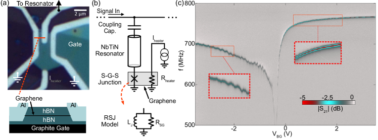
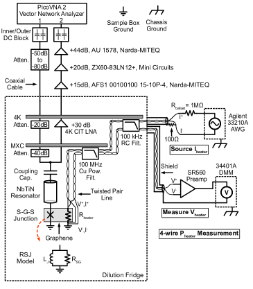
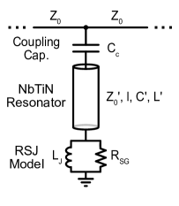
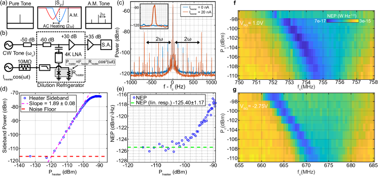
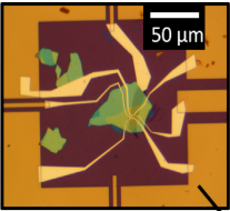
Figure 1 shows a schematic of the device architecture and basic characterization measurements. A gJJ is integrated into a graphene flake of approximate area (Fig. 1(a)). The gJJ consists of a central superconducting contact separated from two symmetrically placed superconducting contacts shorted to the ground plane. Connection is made at the other end of the flake to a heater port used for thermal characterization (see Appendix A and B for details of device fabrication and the measurement architecture). Superconducting aluminum is used for all contacts as it has a small gap relative to other elemental superconductors; we expect this will maximize temperature sensitivity in the sub-Kelvin temperature range of our measurements. To probe the response of the gJJ supercurrent to changes in electron density and temperature, we couple it to an on-chip resonator [6, 13] (Fig. 1(b)). Since the gJJ acts as an additional inductive element, it modifies the resonant frequency, which we monitor through microwave reflectometery. The parameters characterizing the gJJ, the Josephson inductance and subgap resistance , depend strongly on electron density (see also Appendix E). Accordingly, the resonant frequency and spectral width are both highly dependent on the back gate voltage [6] (Fig. 1(c)). Note that we can resolve the resonance over a large range of gate voltages; this allows us to study phenomena arising from electron and hole doping as well as near charge neutrality (). For hole doping (), Fabry-Perot-type oscillations indicate that carrier transport is ballistic in our high-quality graphene sample.
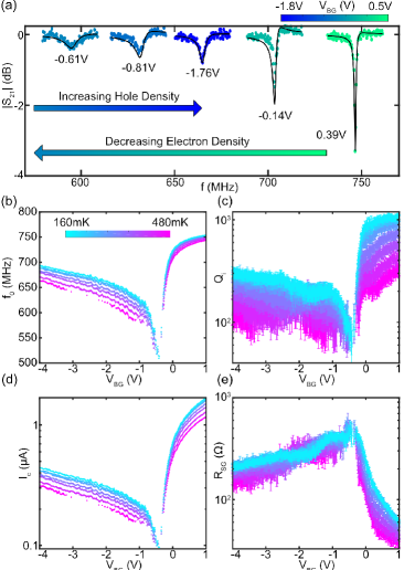
In addition to the electrostatic doping, the circuit resonance is also strongly dependent upon temperature (Fig. 2). When the device temperature increases, the resonance dip shifts to lower frequencies and broadens, reflecting increased losses occurring within the junction. Importantly, the observed shape of the resonance can be fitted using a standard four-parameter Lorentzian fit function at all accessible carrier densities () and temperatures () (see also Appendix C). The high level of agreement between data and the fit (Fig. 2(a)) allows us to relate the deduced resonance parameters to the physical properties of the junction. In particular, shifts of resonant frequency and the overall resonance shape, which is set by internal quality factor , can be related to parameters of the resistively-shunted junction (RSJ) junction model [14], the gJJ critical current and sub-gap resistance [6] (see Fig. 1(b) and Appendix E). These quantities determine the small-signal electrical response of the junction at any temperature and doping level. We note that an estimate of microwave losses in the junction is not accessible from the switching current measurements that have typically been employed in gJJ threshold detection schemes. Fitting the temperature dependence of allows estimation of an induced superconducting gap (see Appendix F). Finally, since we expect the resonator ringdown time to be the limiting time constant in our device, we estimate from the fitted resonance parameters that for all backgate voltages (see Fig. 7).
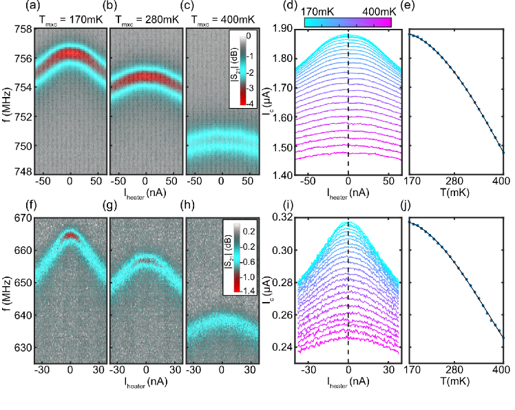
To characterize the thermal properties of the gJJ device, we employ a measurement configuration in which the gJJ is heated internally by applying a DC current to the heater port (Fig. 3). The port electrode is placed sufficiently far from the ground electrodes to preclude supercurrent flow. This configuration allows us to accurately monitor the input power delivered to the graphene flake while simultaneously monitoring the resonance frequency. For different device temperatures and doping, representative changes in the resonance dip are shown in Fig. 3(a-c) and Fig. 3(f-h). By increasing the stage temperature from to , we observe a decrease in the resonant frequency of for holes, compared to for electrons. This is consistent with greater inductive loading (lower ) in the hole regime (see Appendix E). By applying a heater current , the internal flake temperature is increased above , decreasing the resonant frequency. Combined with the measurements taken at different temperatures for calibration (Fig. 3(e,j)) the power vs. temperature characterization and, consequently, the thermal conductivity of the graphene flake can be determined. We use this approach to investigate thermal properties for both electron and hole doping regimes.
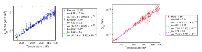
The data we have acquired is consistent with a power law , with electron temperature , stage temperature , scaling exponent and the electron-phonon coupling prefactor (see also Appendix G). We plot (Fig. 4(c)) which shows that the scaling exponents for hole and electron doping are consistent with . We note that our fitting procedures produce only comparably small errors for each of the individual data points and, accordingly, the uncertainty of the extracted scaling exponent is much less than . This enables us to clearly distinguish that the exponent obtained here is not consistent with the or scaling predicted for bulk electron-phonon coupling in reduced dimensions [15, 16]. While an scaling exponent is expected for the electron-phonon coupling of a 3D electron gas [17], these considerations do not apply for our graphene device in which the electron and phonon density-of-states are 2D. Also, we note that the mechanism where hot electrons (or holes) diffuse into the superconducting aluminum leads before thermalization, while in principle possible, is not consistent with our observations (see Appendix H for more detailed discussion).
Measurements of hBN-encapsulated graphene performed previously [5, 8] reveal that (scaled by the area) is about three orders-of-magnitude larger than predictions by simple bulk electron-phonon coupling theory. The magnitude of in our measurements is consistent with these observations. Due to enhanced mobility, hBN-encapsulated graphene is typically in the ballistic scattering limit, in which the carrier mean free path is limited by the device dimension ( in our sample). This observation has led to the hypothesis that the enhanced may arise from “resonant supercollisions” [11, 12] a scenario consistent with the spatially resolved measurements [18, 9]. In this scenario, defects located at edge of the graphene flake locally enhance electron-phonon interactions and open a thermalization pathway that dominates over electron-phonon coupling in the bulk. Spatially-resolved scanning SQUID measurements show an enhancement of surface phonon temperature at graphene edges and close to metal contacts. Theory formulated to explain these results [12] suggests that an scaling exponent should hold down to milli-Kelvin temperatures () in the limit of strong scattering (). In this context, our high precision measurements provide the first clear evidence that an scaling exponent signaling that resonance supercollisions indeed dominate the thermalization in graphene at sub-Kelvin temperatures. We note that further exploration of the device parameter space (e.g. sample size, aspect ratio, disorder) maybe needed to disentangle relations between different microscopic thermalization mechanisms in general.
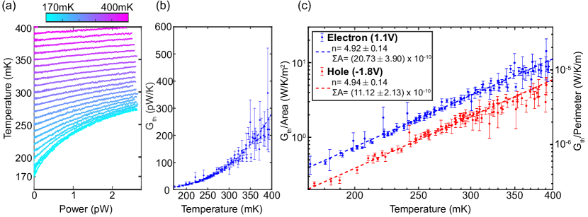
We note that exhibits a power law consistent with for both electron and hole doping, indicating that this mechanism remains dominant in both regimes. Interestingly, the electron- and hole-side prefactors differ by a factor of approximately two (see Fig. 4(c)). A possible explanation for this difference arises from the energy distribution of resonant scattering centers [9]. In this scenario, different scattering centers are activated when the chemical potential of the flake is shifted by the back-gate. Therefore, it is possible that the difference in the prefactors can be attributed to different populations of activated scatterers. Additionally, we note that, in the case of hole doping, the intrinsic p-n junction formed between the graphene region close to the Al contacts (which is always intrinsically n-doped) and the p-doped bulk may also play a role. In this regime, holes from the bulk must pass across the p-n junction in order to efficiently thermalize via resonant scattering centers. Since the p-n junction has a finite transmission probability, it may therefore reduce the overall thermalization rate. We note that attaining an accurate calculation of the thermalization prefactor from first principles is difficult due to effects outlined above and further theoretical work is needed for quantitive comparisons.
In the context of detector technologies, graphene is argued to be a promising platform for future scalable far-infrared or microwave detector-arrays [8, 19]. Its utility for this purpose is typically evaluated on the basis of optimization of several key attributes including response time, responsivity, thermal insulation and multiplexing that, in turn, require simultaneous optimization of multiple device parameters. The hBN-encapsulated graphene devices studied here provide large supercurrents and sub-microsecond response times that allow for continuous monitoring of thermal response, and integration of the resonator readout that permits straightforward frequency-division multiplexing of many devices on a single feedline [20, 21]. Moreover, in our scheme the presence of a separate heater port can be employed for broad-spectrum energy detection. We note that a thermal insulation of the architecture employed here can be achieved at the expense of lowering the mobility in graphene by, for example, placing it directly on the oxide substrate [19] instead of hBN.
Finally, we briefly compare the inductance readout scheme employed here with graphene detectors based on junction switching [8, 22] (between the zero and finite voltage state) as their potential applications may significantly differ. The latter type of detectors register a “count” when the incident photon energy is above a given threshold, and therefore forfeit the possibility of energy spectroscopy provided by the linear, resonantly-coupled graphene detector architecture pursued in this work. Further, threshold detectors intrinsically provide slower response, which is limited by the cooling and resetting of the junction after a photon absorption event. While this type of detector may be a desirable option in the experiments where photon energy and arriving time is known or controlled, the inductance readout detection scheme is more suitable for novel spectroscopy applications of unknown sources [23], including dark matter detection [24, 25, 26, 27] and photon and phonon counting [28] where linear response and ability to fully evaluate detection performance is important (see Appendix I for noise equivalent power characterization).
Acknowledgments: We acknowledge useful discussions with Sophie Li, Matt Matheney, Ewa Rej, and Jonas Zmuidzinas. Funding: This work was supported by NSF through program CAREER DMR-1753306 and Gist-Caltech memorandum of understanding. S.N.-P. also acknowledges the support of DOE-QIS program (DE-SC0019166), IQIM (NSF funded physics frontiers center) and the Sloan foundation. M.L.R acknowledges support from NSF grant NSF-DMR-1806473.
APPENDIX A Fabrication
Fabrication of the superconducting resonator and coupling capacitor proceeds by sputtering a few hundred nanometers of Niobium Titanitum Nitride (NbTiN) on an undoped silicon wafer with 300 nanometers of thermal oxide. Typical superconducting transition temperatures are 14 K. Subsequently, the resonator and coupling capacitor are patterned by electron beam lithography followed by an wet etch and Ar reactive ion etch. The graphene heterostructure is assembled using standard exfoliation and stamping methods and dropped on the resonator chip. 1-D edge contacts between the superconducting metal and graphene heterostructure are patterned by electron beam lithography followed by an Ar reactive ion etch and an electron beam evaporation of the titanium adhesion layer and aluminum contacts.
APPENDIX B Measurement Circuit
A standard transmission measurement is performed in which a swept microwave tone is sent out of Port 1 of a PicoVNA 2 vector network analyzer (VNA) and down through attenuators and stages of the dilution refrigerator. The impedance of the resonator/gJJ device loads the line and scatters the incoming microwave tone. The transmitted portion of the microwave signal is amplified by a first-stage CIT low noise amplifier, and then by three room temperature amplifiers, where it is detected by Port 2 of the VNA.
To improve DC isolation between the device and the VNA, we include inner/outer DC blocks on the ports of the VNA. To vary readout power incident upon to the device, we vary the room temperature attenuation between and . The attenuation at the fridge stages ensures the noise at room temperature is attenuated below the noise floor of the mixing chamber. In the diagram, the attenuators and amplifiers are positioned immediately under the fridge stage to which they are thermally anchored.
The heater measurements in Fig. 3 and Fig. 4 of the main text are performed by applying a DC heater current to the heater port of the graphene flake and reading out the corresponding voltage drop in a 4-wire measurement. To source , an Agilent 33210A AWG outputs a DC voltage for the DC heating measurements of the main text and an AC voltage for the noise equivalent power [29] measurements of section I. Since the ballast resistor is 3 orders-of-magnitude larger than the heater port resistance , the series combination of the AWG and can be well-approximated as a current source . The current travels down PhBr twisted-pair lines to the heater port where it Joule heats the graphene flake. Outside of the fridge, the shield on the twisted pair lines is held at fridge ground. The return line of the twisted pair is grounded through a resistor to a breakout box (not shown) which is also held at fridge ground. The return line terminates at the negative terminal of the AWG. We note that the possible ground loop introduced by the grounding of the twisted pair return line through the resistor does not have an appreciable effect on the measurement.
APPENDIX C Fitting Procedure
Fitting of the resonance feature follows the procedure in Ref. 30. Background-subtracted transmission data is fit to a four-parameter fitting function
Extracted fit parameters include resonant frequency , internal quality factor , coupling quality factor , and asymmetry parameter . Total quality factor is defined as the parallel sum of the dissipation channels . Error bars in Fig. 2b-d correspond to the 95% (2) confidence level calculated from the covariance matrix of the fits. An asymmetry in the resonance circle can cause the diameter of the resonance circle to occur off of the real axis. Such an asymmetry may arise from a non-negligible line inductance or mismatched input/output impedance.
1 Resonance Dependence on
Figure 1(c) shows how the resonance changes as a function of . The maximal tuning of resonance frequency with occurs in the range , , where the . Assuming a parallel-plate capacitance of hBN () and a separation between the graphene flake and backgate, . Since we estimate the area of our graphene flake to be , the maximum sensitivity of our device used as an electrometer is .
APPENDIX D Fitting Procedure for Extraction of RSJ Parameters
To deduce the physical parameters of the gJJ from the fit parameters of the resonance feature, we employ an electrical impedance model of our device which takes the inputs (, ) and numerically solves for junction parameters (, ). is used to estimate the physical parameters of the NbTiN transmission line resonator [31] (See Table 1). The coupling capacitance is estimated by fitting a set of resonances at , numerically solving for , and creating a histogram of extracted values with mode and standard deviation of approximately .
| Coupling capacitor | ||
|---|---|---|
| TLR length | ||
| TLR capacitance per length | ||
| TLR inductance per length | ||
| TLR characteristic impedance | ||
| TLR phase velocity | ||
| Reference characteristic impedance | ||
| Parallel two-port impedance |
APPENDIX E Discussion of Extracted Parameters from Resonance Fits and RSJ Model
As shown in Fig. 7, our fitting and modeling procedure allows several fit and junction parameters to be plotted as a function of backgate voltage and flake temperature .
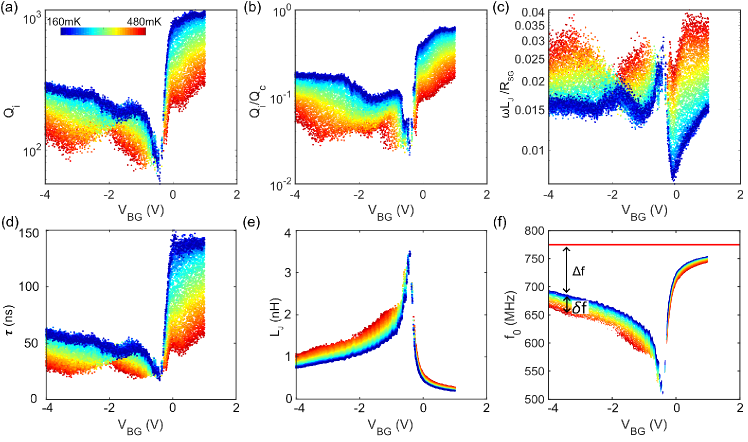
Figure 7(a) shows a dip in at , which is propagated to the other plots Fig. 7(b-d). This dip arises from an asymmetry in the parameter which rotates the resonance circle off the real axis. Such rotations can arise from line impedance mismatches and parasitic couplings [30]. Since is determined primarily by , is sensitive to dissipation in the graphene flake as well as the electromagnetic environment of the flake/resonator assembly. By contrast, and are largely insensitive to these effects, so our thermometry based upon the dispersive shifts of the resonance is also largely insensitive to these effects.
Figure 7(b) shows that our device for all backgate voltages is in the undercoupled limit (), where dissipation occurs primarily within device instead of via the coupling to the microwave lines. The variation of the coupling quality factor is consistent with the circuit model and a constant coupling capacitor pF.
The dispersive shifts of the resonance can be understood from the impedance model shown in Fig. 6, which consists of a transmission line resonator terminated by the junction impedance. This model predicts an unloaded () resonant frequency of as indicated by the solid red line in Fig. 7(f). When a finite inductance loads the transmission line resonator, the resonant frequency decreases. This occurs because a change in the terminating impedance alters the boundary condition at the terminating end of the resonator. In the case of the unloaded resonator, i.e. a resonator, the termination is a short-to-ground, which fixes the boundary voltage at . This enforces the resonance condition that the length of the resonator equals one quarter of the resonant wavelength, i.e. . However, terminating the transmission line resonator in an inductance alters the boundary condition such that the boundary voltage amplitude is fixed at some . This has the effect of enforcing the resonance condition that a quarter-wavelength is larger than the resonator length, i.e. , or, analogously, that the resonant frequency is decreased relative to the unloaded case. The larger the terminating impedance, i.e. the larger , the lower the resonant frequency [6, 31].
Due to higher contact transparency, electron doping should exhibit a larger supercurrent than hole doping. It follows that the electron side should exhibit a smaller than the hole side, and, correspondingly, the electron side should exhibit a smaller decrease in resonant frequency relative to than the hole side. This is consistent with Fig. 7(f) for electron and hole doping, i.e. where is defined as the resonant frequency decrease at .
Increasing the flake temperature further increases and decreases the resonant frequency. A rough estimate of the further decrease of the resonant frequency due to increased temperature is as follows:
As discussed in the section F, typically decreases by 20-30% as the flake temperature is increased from to . From the main text Fig. 3,
Hole Side:
Electron Side:
The change in resonant frequency is therefore consistent with the typical change in . We conclude that the greater magnitude of frequency decrease on the hole side relative to the electron side follows as a straightforward result of the greater inductive loading of the transmission line resonator.
As shown in Fig. 7(c), is a common figure-of-merit for RF-driven Josephson junctions [32]. It compares the impedance of the dissipationless supercurrent branch to the dissipative resistive branch. A smaller value of denotes a less dissipative device. At , within a factor of 2. As the temperature rises to , increases to 3%. This is consistent with decreases in raising the impedance of the dissipationless branch and driving more current through the dissipative branch, as indicated by the degrading quality factor with increasing flake temperature (see Fig. 2(c)).
APPENDIX F vs. Fits and Extraction of Induced Superconducting Gap
Due to the measurement architecture employed here, we cannot perform 4-wire measurements directly on the gJJ to estimate the induced superconducting gap . Instead, we perform a fitting procedure based upon the temperature dependence of the critical current .
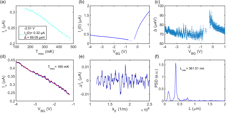
The vs. data in Fig. 2(d) is fit to extract physical parameters. The fit function we employ describes the supercurrent that arises from thermally populating the Andreev bound states (ABS) in a ballistic junction [33].
The two fit parameters correspond to the physical parameters , the zero-temperature critical current, and , the induced superconducting gap. An example fit is shown in Fig. 8(a).
In Fig. 8(b), modulation of the fit parameter with on the hole side is consistent with -type Fabry-Perot interference as discussed in the main text and Fig. 1(c). Following the standard method for determining Fabry-Perot cavity length in ballistic graphene, we subtract the slowly varying background with a fit to a -order polynomial (see Fig. 8(d-e)) and take the power spectral density (see Fig. 8(f)). The large peak in the power spectral density is consistent with a Fabry-Perot cavity length of . Structure on the electron side could be caused by an -type Fabry-Perot cavity [34].
From Fig. 8(c), we can make a coarse estimate of the induced superconducting gap . However, further measurements are needed to determine whether the finer structure of Fig. 8(c) is due to the physics of the S-G-S junction or an artifact of the fitting procedure. Toward this end, it would be useful to perform simultaneous RF characterization and DC multiple-Andreev reflection measurements on a gJJ sample [6].
APPENDIX G Power vs. Temperature Fitting Procedure
To obtain the vs. in Fig. 4(c), we first perform piece-wise linear fits of the curves of Fig. 4(a). Subsequently, we perform a nonlinear least squares fit of the vs. to the fitting function
| (1) |
with free fit parameters the scaling exponent and the electron-phonon coupling. The errors in the free fit parameters correspond to the (95%) errors obtained from the nonlinear least squares fit. On the electron side, we include an exclusion criteria at the limit of the temperature resolution of our device. This criteria does not appreciably change the extracted or . Without the exclusion criteria the extracted fit parameters are and . With the exclusion criteria, the extracted fit parameters are and .
APPENDIX H Other thermalization pathways
In this section, we briefly discuss alternative thermalization pathways that can occur in our experimental geometry. While they indeed occur, we note that the thermal conductance corresponding to these alternative pathways are all too small to explain our measurements.
Thermalization via bulk phonons
The bulk phonons are often invoked as the main source of electron thermalization in graphene. However, besides having a different exponent ( or not agreeing with our data, see Fig. 10), the cooling rate via bulk graphene phonons is too small to explain experimental findings. As discussed in previous literature, the typical thermal conductance expected from bulk phonons is two orders of magnitude smaller than the measured data. We note that, in this context of the overall cooling rate, our measurements are roughly in line with previous graphene-hBN experiments.
Thermalization in Aluminum leads: Another possibility is that the hot electrons enter Al leads. While the tunneling of electrons (or holes) in a superconductor is expected to be suppressed due to the existence of a finite single-particle gap, previous work found that this process can still be sizable when using Aluminum electrodes. The critical distinction between our study and previous work using Aluminum contacts (see, for example, Ref. [35]), is that we used Al only as immediate contact to graphene (Fig. 11), and beyond that, the electrodes used in our experiment are made from Niobium Titanium Nitride (NbTiN) which has a much larger superconducting gap ( meV). In this context, the amount of heat that could “leak” into Aluminum contacts is much lower compared to measured values of thermal conductance. A total volume of Aluminum in our device is only approximately m3. By considering the established value for electron-phonon coupling in Aluminum ( W/K5m3, see Ref. [36]) the corresponding P. vs T dependence is expected to follow . Here eV is Aluminum superconducting gap measured in our experiments and a numerical pre-factor of 0.98 is estimated in Ref. [37]. At mK this rate corresponds to W, approximately two orders of magnitude smaller than the observed thermalization rates at our lowest temperatures.
APPENDIX I Noise Equivalent Power
1 Theory
A key figure-of-merit for linear power detectors is noise-equivalent power (). A power-to-voltage detector has a responsivity , such that
In the linear-response regime, i.e. for small applied power, this expression simplifies to
In this regime, the of a power-to-voltage detector (in units of ) can be defined as that power spectral density at the device input which produces the measured voltage spectral density at the output:
The above expression suggests two immediate ways to measure the . One is to measure the voltage spectral density at the output and the device responsivity . Another is to measure the applied power at the input , and the at the output as suggested by rearranging the above expression
In the above equation, the is in units of and . The latter expression is true since we have implicitly assumed is that input power that produces the measurable signal. In our case, only one quarter of the heat power injected at the heater port produces the measured sideband signal.
2 Experimental Design
To measure the , we use the measurement setup in Fig. 9(a,b) and perform the following procedure:
-
•
We apply a carrier tone on the microwave line (Fig. 9(a), first panel). The parameter is the transfer function which determines the magnitude and phase of the signal at the output. Thus, a carrier tone at the resonant frequency, i.e., at the maximal dip of the parameter will have a smaller transmitted magnitude than a carrier tone placed off-resonance.
-
•
Measurement of is achieved by sourcing a current to the heater port and measuring the voltage drop over the heater port in a 4-wire lock-in measurement. Since we apply an AC heater current , it follows that . Only the term in the final expression contributes to the sideband signal.
-
•
Applying an AC heat power to the heater port modulates the parameter between unheated and heated states (Fig. 9(a), second panel). Consistent with the heating measurements performed in the main text, the heated state has a lower resonant frequency and lower quality factor than the unheated state. The component of the input power modulates the flake temperature at . Thus, modulation of the resonance feature will occur at .
-
•
Placing the frequency of the carrier tone within the bandwidth of the modulated resonance feature will amplitude modulate the carrier, producing sidebands spaced at from the carrier (Fig. 9(a), second and third panel). Provided that the device is in the linear-response regime, the voltage of the sidebands will increase in proportion to applied heat power, i.e. . It follows that the power of the sidebands will increase as .
-
•
The amplitude-modulated carrier is read out by a spectrum analyzer (Fig. 9(a), third panel). The signal-to-noise ratio of the sideband is used to calculate the . We note that only one sideband is used in the measurement.
3 Sideband Spectrum
In Fig. 9(c), we see that application of an AC heater current of magnitude nA results in sidebands at 2 offset from the carrier, where . In addition to the 2 sidebands, sidebands at multiples of the line frequency frequency are present. Additionally, there are sidebands at approximately down from the 2 sidebands. This can be explained by a small DC offset in the heater current.
With increasing heater power, the magnitude of the sidebands saturates at a value consistent with expectations. It is straightforward to show that a resonance dip of generates a maximum amplitude modulation index , which should produce sidebands lower than the carrier. This is in agreement with the measured sideband magnitude that is lower than the carrier.
4 Sideband Scaling
In the linear response regime, . Therefore, the sideband signal as measured on the spectrum analyzer (in power units) should scale as , or by . This is seen in Fig. 9(d) for applied heat in the range to , where the slope of fit at low- is consistent with a scaling exponent . This confirms that our measurement is in linear-response regime at low . For greater applied , the sideband power saturates as the amplitude modulation reaches the full maximum of the resonance dip.
5 vs.
In the linear response regime, the is constant with respect to since . This is shown Fig. 9e for . As stated above, the rises for as the saturates while continues to increase.
6 vs. Carrier Frequency and Carrier Power
To explore the as a function of the carrier tone, we generate a heat map with swept carrier frequency and carrier power (Fig. 9(f,g)). For the lowest carrier powers, the is minimized for carrier frequencies close to the resonance minimum, where the responsivity of the resonance to applied heater power is greatest and therefore the amplitude modulation of the carrier is greatest. As the carrier power is increased, the junction is driven to nonlinearity, resulting in a resonance dip with a steep falling edge and a shallow rising edge. This has the effect of enhancing the on the falling edge and reducing it on the rising edge. For carrier powers , the quality factor of the resonance feature is degraded to such an extent that the amplitude modulation of sideband is reduced and the increases. The reaches a minimum value of for a carrier power dBm and carrier frequency MHz.
7 Detection Limits
The measured minimum noise-equivalent power . It is limited by the noise of the 4K cryoamp and is larger than the thermal fluctuation-limited at . At , the projected thermal fluctuation-limited , assuming that the dependence of holds down to these temperatures [29, 38]. The corresponding thermal fluctuation-limited energy resolution , assuming the projected thermal time constant , , .
References
- [1] Fong, K. C. & Schwab, K. C. Ultrasensitive and Wide-Bandwidth Thermal Measurements of Graphene at Low Temperatures. Physical Review X 2, 031006 (2012).
- [2] Fong, K. C. et al. Measurement of the Electronic Thermal Conductance Channels and Heat Capacity of Graphene at Low Temperature. Physical Review X 3, 041008 (2013).
- [3] Borzenets, I. V. et al. Ballistic Graphene Josephson Junctions from the Short to the Long Junction Regimes. Physical Review Letters 117, 237002 (2016).
- [4] Calado, V. E. et al. Ballistic Josephson junctions in edge-contacted graphene. Nature Nanotechnology 10, 761–764 (2015).
- [5] Draelos, A. W. et al. Supercurrent Flow in Multiterminal Graphene Josephson Junctions. Nano Letters 19, 1039–1043 (2019).
- [6] Schmidt, F. E., Jenkins, M. D., Watanabe, K., Taniguchi, T. & Steele, G. A. A ballistic graphene superconducting microwave circuit. Nature Communications 9, 4069 (2018).
- [7] Borzenets, I. V. et al. Phonon Bottleneck in Graphene-Based Josephson Junctions at Millikelvin Temperatures. Physical Review Letters 111, 027001 (2013).
- [8] Lee, G.-H. et al. Graphene-based Josephson junction microwave bolometer. Nature 586, 42–46 (2020).
- [9] Halbertal, D. et al. Imaging resonant dissipation from individual atomic defects in graphene. Science 358, 1303–1306 (2017).
- [10] Saira, O.-P., Zgirski, M., Viisanen, K. L., Golubev, D. S. & Pekola, J. P. Dispersive Thermometry with a Josephson Junction Coupled to a Resonator. Physical Review Applied 6, 024005 (2016).
- [11] Kong, J. F., Levitov, L., Halbertal, D. & Zeldov, E. Resonant electron-lattice cooling in graphene. Physical Review B 97, 245416 (2018).
- [12] Tikhonov, K. S., Gornyi, I. V., Kachorovskii, V. Y. & Mirlin, A. D. Resonant supercollisions and electron-phonon heat transfer in graphene. Physical Review B 97, 085415 (2018).
- [13] Wang, J. I.-J. et al. Coherent control of a hybrid superconducting circuit made with graphene-based van der Waals heterostructures. Nature Nanotechnology 14, 120–125 (2019).
- [14] Tinkham, M. Introduction to Superconductivity (Publisher: Dover Publications, 2004).
- [15] Viljas, J. K. & Heikkilä, T. T. Electron-phonon heat transfer in monolayer and bilayer graphene. Physical Review B 81, 245404 (2010).
- [16] Chen, W. & Clerk, A. A. Electron-phonon mediated heat flow in disordered graphene. Physical Review B 86, 125443 (2012).
- [17] Roukes, M. L., Freeman, M. R., Germain, R. S., Richardson, R. C. & Ketchen, M. B. Hot electrons and energy transport in metals at millikelvin temperatures. Physical Review Letters 55, 422–425 (1985).
- [18] Halbertal, D. et al. Nanoscale thermal imaging of dissipation in quantum systems. Nature 539, 407–410 (2016).
- [19] Kokkoniemi, R. et al. Bolometer operating at the threshold for circuit quantum electrodynamics. Nature 586, 47–51 (2020).
- [20] Day, P. K., LeDuc, H. G., Mazin, B. A., Vayonakis, A. & Zmuidzinas, J. A broadband superconducting detector suitable for use in large arrays. Nature 425, 817–821 (2003).
- [21] Wandui, A. et al. Thermal kinetic inductance detectors for millimeter-wave detection. Journal of Applied Physics 128, 044508 (2020).
- [22] Walsh, E. D. et al. Graphene-Based Josephson-Junction Single-Photon Detector. Physical Review Applied 8, 024022 (2017).
- [23] Lara-Avila, S. et al. Towards quantum-limited coherent detection of terahertz waves in charge-neutral graphene. Nature Astronomy 3, 983–988 (2019).
- [24] Hochberg, Y., Kahn, Y., Lisanti, M., Tully, C. G. & Zurek, K. M. Directional detection of dark matter with two-dimensional targets. Physics Letters B 772, 239–246 (2017).
- [25] Kim, D., Park, J.-C., Fong, K. C. & Lee, G.-H. Detecting keV-Range Super-Light Dark Matter Using Graphene Josephson Junction. arXiv:2002.07821 [cond-mat, physics:hep-ex, physics:hep-ph] (2020). eprint 2002.07821.
- [26] McAllister, B. T. et al. The ORGAN experiment: An axion haloscope above 15 GHz. Physics of the Dark Universe 18, 67–72 (2017).
- [27] Baracchini, E. et al. PTOLEMY: A Proposal for Thermal Relic Detection of Massive Neutrinos and Directional Detection of MeV Dark Matter. arXiv:1808.01892 [astro-ph, physics:hep-ex, physics:physics] (2018). eprint 1808.01892.
- [28] Roukes, M. L. Yoctocalorimetry: Phonon counting in nanostructures. Physica B: Condensed Matter 263–264, 1–15 (1999).
- [29] Mather, J. C. Bolometer noise: Nonequilibrium theory. Applied Optics 21, 1125–1129 (1982).
- [30] Geerlings, K. et al. Improving the quality factor of microwave compact resonators by optimizing their geometrical parameters. Applied Physics Letters 100, 192601 (2012).
- [31] M. Pozar, D. Microwave Engineering, 4th Edition (Wiley, 2011).
- [32] Van Duzer, T. & W Turner, C. Principles of Superconductive Devices and Circuits (Pearson, 1998).
- [33] Lee, G.-H., Kim, S., Jhi, S.-H. & Lee, H.-J. Ultimately short ballistic vertical graphene Josephson junctions. Nature Communications 6, 6181 (2015).
- [34] Nanda, G. et al. Current-Phase Relation of Ballistic Graphene Josephson Junctions. Nano Letters 17, 3396–3401 (2017).
- [35] Voutilainen, J. et al. Energy relaxation in graphene and its measurement with supercurrent. Physical Review B 84, 045419 (2011).
- [36] Giazotto, F., Heikkilä, T. T., Luukanen, A., Savin, A. M. & Pekola, J. P. Opportunities for mesoscopics in thermometry and refrigeration: Physics and applications. Reviews of Modern Physics 78, 217–274 (2006).
- [37] Timofeev, A. V. et al. Recombination-Limited Energy Relaxation in a Bardeen-Cooper-Schrieffer Superconductor. Physical Review Letters 102, 017003 (2009).
- [38] Moseley, S. H., Mather, J. C. & McCammon, D. Thermal detectors as x-ray spectrometers. Journal of Applied Physics 56, 1257–1262 (1984).