Non-local Andreev reflection through Andreev molecular states in graphene Josephson junctions
Abstract
We propose that a device composed of two vertically stacked monolayer graphene Josephson junctions can be used for Cooper pair splitting. The hybridization of the Andreev bound states of the two Josephson junction can facilitate non-local transport in this normal-superconductor hybrid structure, which we study by calculating the non-local differential conductance. Assuming that one of the graphene layers is electron and the other is hole doped, we find that the non-local Andreev reflection can dominate the differential conductance of the system. Our setup does not require the precise control of junction length, doping, or superconducting phase difference, which could be an important advantage for experimental realization.
Quantum entangled particles have numerous potential applications in fields such as quantum communications or quantum cryptography. Thus, practical schemes of producing entangled particles are of fundamental interest [1]. One of the most promising candidates for creating entangled electron states is based on spin singlet Cooper pairs. It was proposed that if the electrons of a Cooper pair can be extracted coherently and separated spatially, they can serve as a source of entangled electrons [2, 3]. This process is known as Cooper pair splitting (CPS). As discussed in, e.g., Refs. [4, 5], the key physical process to achieve CPS is the non-local or crossed Andreev reflection (CAR).
Although the first observations of Cooper pair splitting were made in metallic nanostructures [6, 7], devices that use two quantum dots (QDs) have garnered the most attention in this field. The charging energy on the QDs prohibits the double occupancy on each dot, leading to the suppression of electron cotunneling (EC). EC is a competing process with CAR and it should be suppressed in order to achieve CPS. Experimentally CPS has been achieved in QD devices realized in InAs and InSb nanowires [8, 9, 10, 11, 12, 13], carbon nanotubes [14, 15], graphene based QDs [16, 17, 18], and recently in 2DEGs [19]. Alongside the experimental effort, substantial theoretical work has also been devoted to the study of CPS in QD based devices [2, 20, 3, 21, 22].
A different approach to suppress EC with respect to CAR makes use of features in the density of states of semiconductors [23, 24]. Since this approach does not necessitate QDs, it should make the fabrication of CPS devices simpler. Regarding monolayer graphene, Ref. [23] predicted that pure CAR could be achieved in a -type graphenesuperconductor-type graphene junction, if the doping of the graphene is smaller than the superconductor pair potential . In this case, the vanishing density of state of graphene at the Dirac point allows the elimination of processes that suppress CAR. However, due to the charge fluctuations around the Dirac point, which are usually larger [25, 26] than the value of of most superconductors, such a low doping is difficult to achieve experimentally. The problem of charge fluctuations can be mitigated, to some extent, by using bilayer graphene [27], because the larger density of states allows a better control of residual doping levels [28, 27]. Recently, the signatures of CPS have also been observed in multi-terminal ballistic graphene-superconductor structures [29]. Another recent theoretical proposal [30, 31] suggested that the CAR probability can be enhanced in a device where the central region consists of two, coupled one-dimensional superconductors and two normal leads are attached on each side to one of the superconductors. The central region effectively constitutes a superconducting QD. The CAR can be resonantly enhanced by tuning the superconducting phase difference between the one-dimensional superconductors to and then adjusting the chemical potential of the superconductors.
In this work we propose that an approach based on Andreev molecular states [32, 33] can also help to achieve CAR dominated transport. It was suggested that Andreev bound states (ABSs) in closely spaced Josephson junctions can overlap and hybridize forming Andreev molecular states (AMSs). We study the possibility of CPS in a setup that harbors AMSs. The device consists of two graphene Josephson junctions displaced vertically with respect to each other, (see Fig. 1) such that the ABSs in the two junctions can hybridize. This type of graphene JJ has recently been studied experimentally in Ref. [34], focusing on superconducting interference device type operation and quantum Hall physics. We calculate the non-local, non-equilibrium differential conductance through the device, when two normal leads are weakly connected to the graphene layers, as shown in Fig. 1. Our most important finding is that CAR can be larger than EC even if the doping of the graphene layers is significantly larger than the value of . Therefore, the CAR should be less affected by charge puddles, which are present in graphene at low doping.
I The model
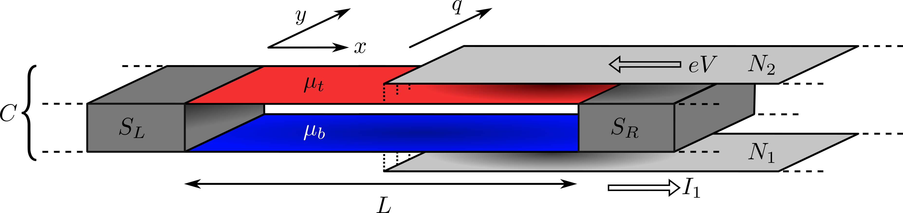
The schematics of the proposed four-terminal device is shown in Fig. 1. Two graphene monolayers (red and blue) of length are placed above each other. They are separated by an insulator such as hBN or vacuum in the center of the device, i.e., for , meaning that there is no direct electrical contact between these two layers vertically. Two superconducting leads, and (dark gray) are attached to the edges of the top and bottom graphene layers, at and . In addition, two normal leads (light gray) and are weakly coupled to the middle () of the top and the bottom graphene layer, respectively. We note that a similar layout for a single graphene JJ junction was used in Ref. [35] to determine the energy spectrum of ABSs.
In our calculations the description of both the normal and the superconducting regions is based on the nearest-neighbor tight-binding model of graphene with in-plane hopping amplitude . The top and bottom graphene layers and the superconducting leads constitute the central region of the device, described by the Hamiltonian
| (1) |
Here is the Hamiltonian of undoped monolayer graphene, is the Hamiltonian of the superconducting leads in the non-superconducting state. The leads and are modeled with Bernal stacked multilayer graphene, with out-of plane hopping amplitude . We assume that the top and bottom graphene layers are perfectly aligned and denote the doping by [] in the top [bottom] layer, while is the doping in and . describes the coupling between the graphene layers and the superconducting leads with hopping amplitude , corresponding to a perfectly transparent interface.
Before superconductivity is introduced, the total Hamiltonian of the system reads
| (2) |
where is the Hamiltonian of the normal leads , with . The leads are also modelled by monolayer graphene and their doping is kept fixed at eV. We checked that the results discussed below do not strongly depend on . describes the coupling between and the corresponding graphene layer (see Fig. 1).
To describe the transport properties of this system when the leads and are superconducting, we used the approach based on the Bogoliubov–de Gennes Hamiltonian. This can be compactly written as
| (3) |
where is the Fermi energy, is the excitation energy, and are electron and hole wave functions, respectively. is a matrix which only has non-zero elements between degrees of freedom that belong to either or . To describe superconductivity, an -wave pairing potential is used, which is nonzero only in the superconducting leads and changes in a step-function manner at the normal-superconducting interface: , where is the Heaviside function, and is the superconducting phase difference between and . The step-function change of the pair-potential at the boundary is valid if [36]. Here and are the Fermi wavelength in the superconducting leads and central graphene layers and is the (in-plane) ballistic superconducting coherence length, m/s being the Fermi velocity of monolayer graphene. We use highly doped superconducting leads with eV, therefore the above condition is satisfied in all our calculations. Since the in-plane and out-of plane hopping amplitudes in Bernal stacked multilayer graphene are different, it is intuitive to define an effective superconducting coherence length associated with the out-of-plane hopping in the superconducting leads. One can expect that interlayer Andreev reflection from the top to the bottom graphene layers is only significant if , where is the vertical distance between these layers. We explain how is estimated in Supplementary Information (SI), here we only mention than in all subsequent calculations .
In the transport calculations we assume that a voltage is applied (with respect to ) to the top normal lead and the current is measured in the bottom normal lead , as shown in Fig. 1. We calculate the non-local differential conductance which depends on CAR. We are primarily interested in the case of wide graphene layers, where exact termination of the edges does not matter because the transport properties are determined by bulk states. Using hard wall boundary conditions [37, 38], the transverse wavenumber parallel to the direction is a good quantum number, see the SI for further details. The numerical calculations discussed below were performed using the tight-binding framework implemented in the EQuUs [39] package.
II Andreev molecular states
The Andreev reflection of quasiparticles at the graphene-superconductor interfaces leads to the formation of correlated electron-hole states known as Andreev bound states, [36, 40, 41, 42, 35, 43] with energies . Their presence in the proximitized graphene layers means that an induced gap appears in the graphene layers, which is smaller than the pairing potential of the superconductors. If the superconducting phase difference is fixed, in ballistic systems the magnitude of is determined by the smaller of two energy scales, namely, the bulk gap and the Thouless energy .
For , when , i.e., in the short junction regime . In the opposite case , the dominant energy scale is ; this is the long junction regime where is considerably smaller than . Note that the ratio of and can also be expressed as , so that the short junction regime corresponds . In this work, we study devices with Thouless energy between and . Junctions with in this range correspond to the intermediate length regime, where analytic results valid in the short [36] or long [40] regime of a Josephson junction (JJ) consisting of a single graphene layer do not strictly apply. Taking meV, the aforementioned values correspond to between and nm.
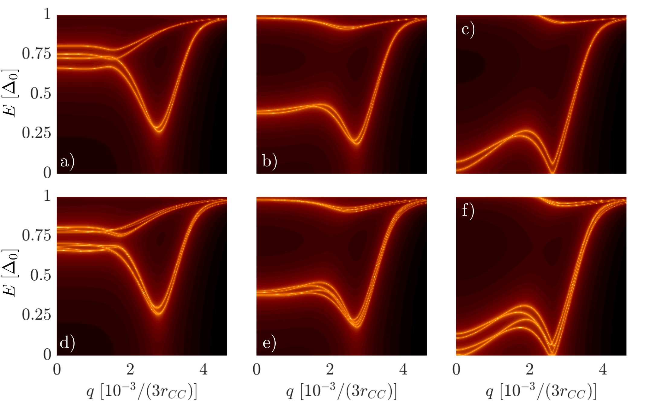
One can expect that in the setup shown in Fig. 1, the ABSs formed in the two graphene layers can hybridize, leading to the formation of Andreev molecular states (AMSs) [32, 33]. In order to see the effects of ABS hybridization, we start by considering the properties of ABSs formed in individual layers, i.e., when one of the graphene layers, e.g., the bottom one is disconnected from the superconductors and only the top one is connected. We also disconnect the lead and calculate the Green’s function of the resulting graphene JJ. The spectrum of the ABSs is determined performing local density of states (LDOS) calculations for energies . The LDOS is calculated as the sum of the LDOS of electron and hole type quasiparticles , where is the imaginary part of the retarded Green’s function. The LDOS is evaluated on unit cells of the top layer around . In Figs. 2(a)-(c) we show results for superconducting phase differences and , using meV and . One can clearly see the appearance of multiple ABSs. Above there is an energy range where no ABSs are present indicating the induced gap . One can observe that as increases from to , the induced gap decreases and at the induced gap is closed. This can be shown analytically in both the short [36] and long [40] junction regime and also agrees with the experimental results of Ref. [35].
Turning now to the bilayer setup of Fig. 1, the distance between the graphene layers is taken to be nm in our calculations, while we found that nm (see SI). Since , the coupling between the ABSs can lead to the formation of Andreev molecular states [32, 33]. This is shown in Figs. 2(d)-(f), where one can see the LDOS calculated in the top graphene layer. At this stage the normal leads and are not yet connected to the graphene layers. For AMSs with energies the relatively weak hybridization leads to only minor modifications of the LDOS, c.f. Figs. 2(a)-(c). However, for there are AMSs with energy which are more strongly modified by interlayer hybridization [Fig. 2(f)]. One can also see that, similarly to the case of ABSs [Figs. 2(a)-(c)], the magnitude of in the presence of AMSs can be tuned by changing [Figs 2(d)-(f)].
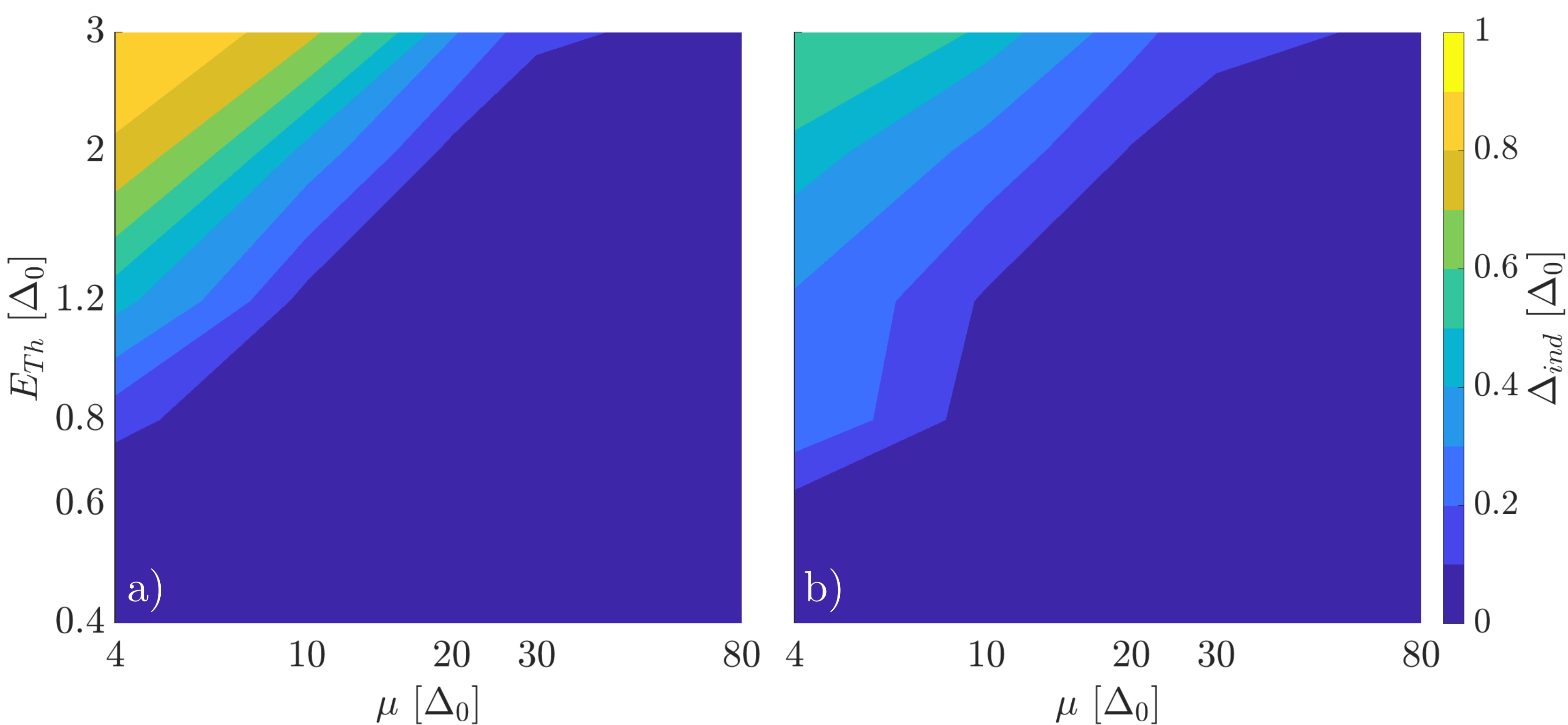
One can expect that in order to have a finite interlayer transmission of electrons from to in the bias window , has to be smaller than . Therefore, is an important parameter of the device. We calculated as a function of the doping and , where , see Fig. 3. The value of is extracted from LDOS calculations by determining the minimum of the AMS spectrum. We find that for and the induced gap is suppressed [Fig. 3(a)]. However, for larger values of a general observation is that is comparable to for low doping, but increasing leads to the reduction of . For large enough doping the induced gap can be suppressed regardless of the Thouless energy for the values we studied. In short, the condition is satisfied for a wide range of (, ) values. Note that tuning the doping changes not only , but also the number of the AMSs. Furthermore, as illustrated in Figs. 2(d)-(f), by increasing the AMSs are shifted deeper into superconducting gap and decreases [Fig. 3(b)]. We find that in these ballistic devices for the induced gap disappears regardless of the value of .
III Differential conductance
We now discuss the transport through the central region of the device when the normal leads and are attached, as shown in Fig. 1. We are interested in the dependence of in on the applied voltage to . We restrict our study to voltages , therefore one expects that the transport is mediated by the AMSs in the junction. We use the Keldysh non-equilibrium Green’s function technique [44, 45, 46, 47, 48] to calculate for a given and then sum the contributions of the different values, see the SI for more details. The differential conductance is given by
| (4) |
where is a Pauli matrix acting in the electron-hole space and is the bottom lead–central region lesser Green’s function. To lighten the notations, the dependence of is not written explicitly. The differential conductance can be evaluated as
| (5) |
where is the width of the junction in the direction. All calculations are performed at K temperature.
In order to obtain an insight into the transport properties of this setup, let us first consider a simple model: we assume that only a single AMS of energy is present, which extends over both graphene layers in the central region. We neglect the dependence of the AMS and assume that coupling between () and bottom (top) graphene layers is weak. According to the calculations detailed in the SI, the differential conductance can be approximated by
| (6) |
where are level broadenings [49] due to the coupling of the electron [hole] () part of the AMS to the states in at energy , and . Eq. (6) shows that the presence of an AMS results in a resonant peak of Lorentzian lineshape in the differential conductance, at . The signature of CAR dominated transport is , meaning that an injected electron in is transmitted as a hole into . The sign of is determined by the numerator in Eq. (6), which depends on the difference between the level broadening of electron- and hole-like degrees of freedom of the AMS.
In the tunneling limit depends on the product of the LDOS of the electron (hole) component of the AMS and of the attached leads . Since the leads are metalic, their LDOS is constant. Therefore depends mainly on the difference of the LDOS of the electron and hole type quasiparticles in the AMS. One can expect that this can be changed by two means: firstly, by tuning the doping of the two graphene layers. Secondly, since the AMS wave functions depend on the superconducting phase difference , the LDOS can also be changed by tuning . Thus, this simple model suggests that one has two experimental knobs to tune the interlayer transmission and try to achieve CAR dominated transport.
As it can be seen in Fig. 2, for finite doping of the graphene layers, multiple AMS are present in our setup. The result given in Eq. (6) can be easily generalized to this case (see the SI). One finds that defined in Eq. (4) reads
| (7) |
where the summation runs over the number of the AMSs, depends on the product of the wave functions of the th and th AMS and . The terms are Lorentzian resonances, this is the type of contribution we have already discussed when we derived Eq. (6). The terms correspond to a “cross-talk” between different AMSs and they are affected by interference effects between different AMSs. Therefore, in general, depends both on the LDOS and on the interference of the quasiparticle components of the AMSs.
Note, that in Refs. [23, 24] the enhancement of the probability of CAR is related to the DOS of the semiconducting leads, which are attached to a central superconducting strip, and their different doping. In our setup the leads are assumed to be metallic and their doping does not play an important role. Moreover, as we discussed above, in our case quasiparticle interference also affects , but as we will show in Sec. IV it does not lead to the type of resonant enhancement of CAR as in Refs. [30, 31]. These considerations clearly show the difference between our proposal and those of Refs. [23, 24, 30, 31].
IV Negative non-local Andreev reflection
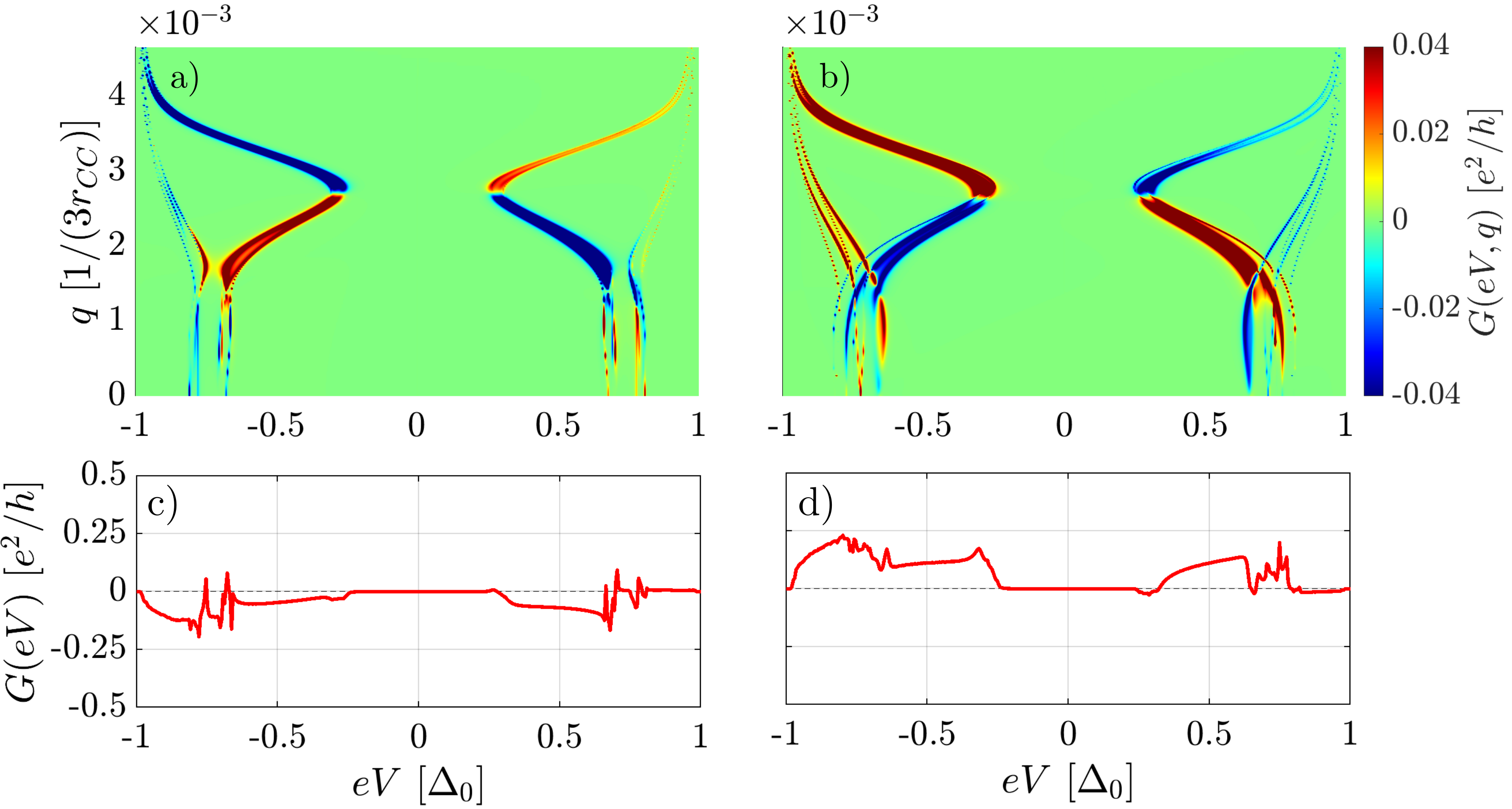
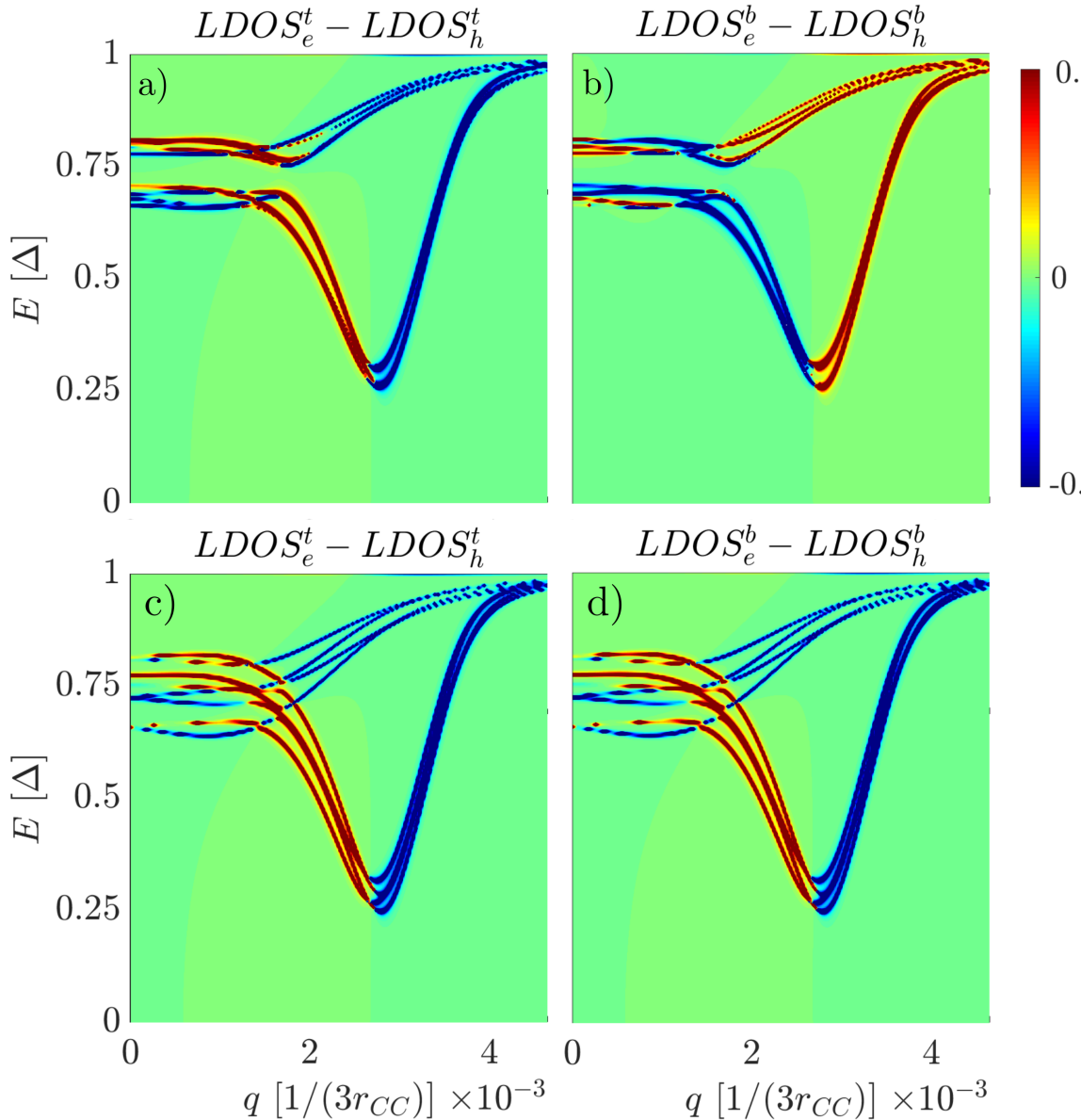
We start with calculations which illustrate the complex interplay of LDOS and interference related effects in the differential conductance. In Figs. 4 we show the LDOS difference of the electron and hole quasiparticles of AMSs () in the top (bottom) graphene layers. These results were obtained in the same way as the total LDOS in Fig. 2(d)-(f), i.e., evaluated on unit cells around . We consider two cases: (asymmetric doping) and (symmetric doping) and the parameters of the calculations correspond to the case shown in Fig. 2(d). In a given layer the sign of depends on both the energy and the wavenumber . However, one can clearly observe that for asymmetric doping has opposite sign to . On the other hand, for symmetric doping , which can be expected based on the inversion symmetry of the system. Since more than one AMSs gives contributions to , these results cannot be directly related to individual broadening differences , but they do illustrate the important effect of the doping of the two graphene layers. Furthermore, using the arguments put forward below Eq. (6), these results suggest that the sum of the terms in Eq. (7) gives a negative (positive) contribution to the differential conductance for asymmetric (symmetric) doping profile.
The contributions of the terms in Eq. (7) is more difficult to visualize, but our numerical calculations indicate that they give an equally important contribution to . To illustrate this point, in Figs. 5(a) and (b) we show the -resolved non-local differential conductance for asymmetric and symmetric doping, respectively, and weakly coupled normal leads and . We used the same parameters as for the calculations in Fig. 4. The non-zero matrix elements of and are on the order , where is the interlayer coupling in Bernal stacked graphene. The general features in closely resemble the LDOS in Fig. 4, showing the important role of the AMSs in the non-local conductance for this relatively weak coupling between , and the corresponding graphene layers. can be both positive and negative as a function of , which indicates that the LDOS difference of the electron and hole quasiparticles, shown in Fig. 4, is not the only factor affecting it. However, as one can see by comparing Figs. 5(c) and (d), we find that the total non-local differential conductance is mostly negative (positive) for asymmetric (symmetric) doping.
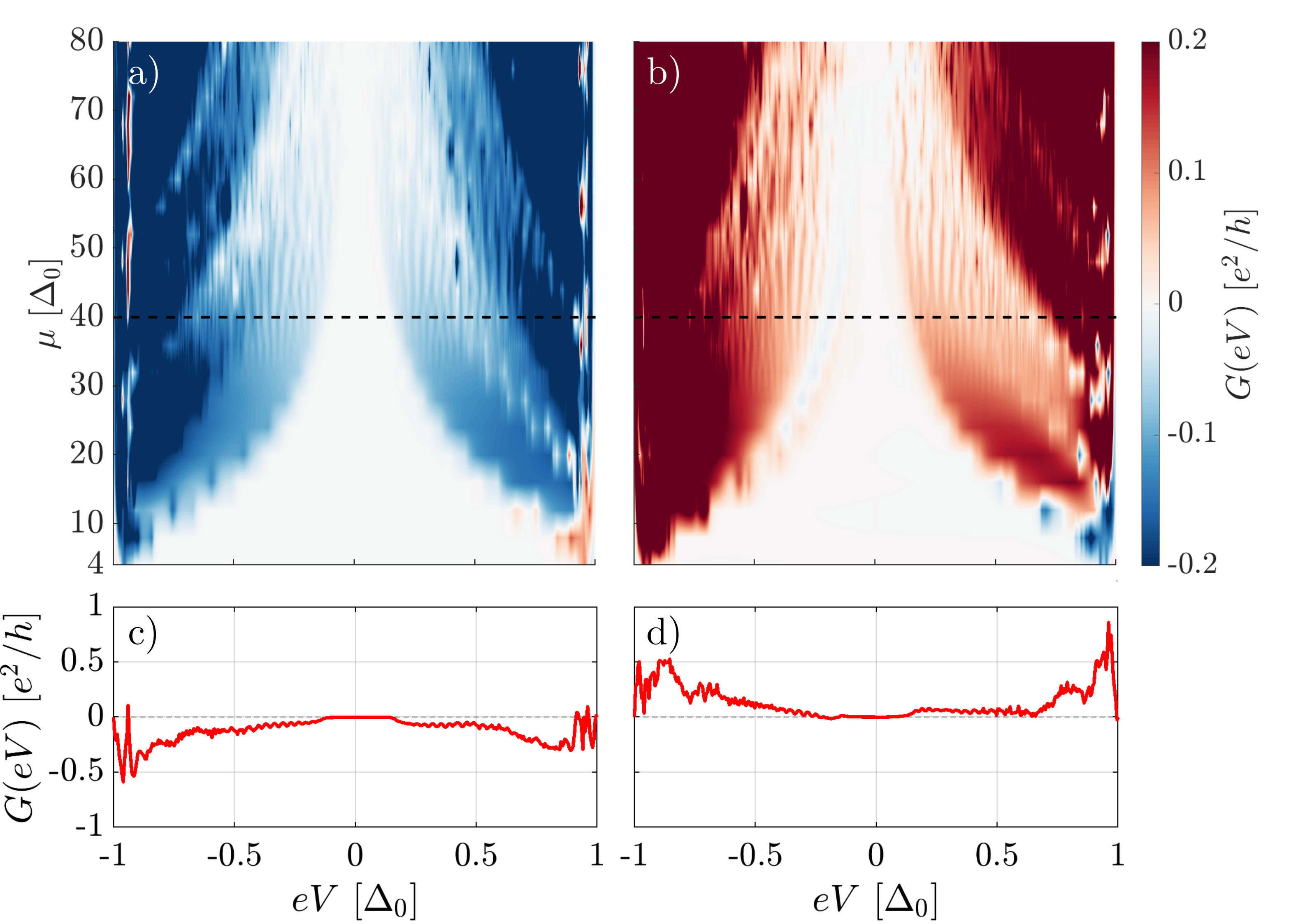
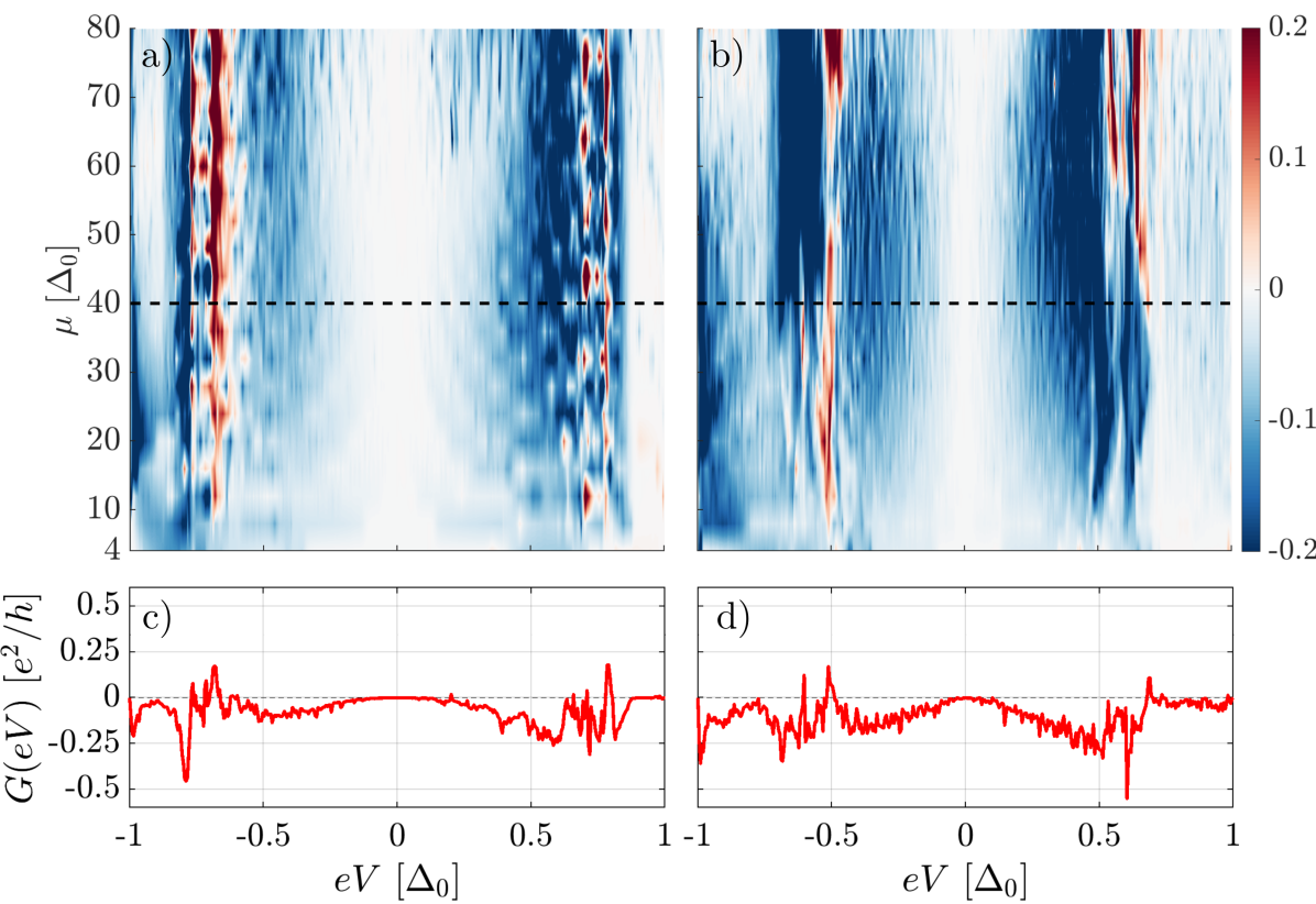
Next, we study the dependence of on the magnitude of the doping of the layers. In Fig. 6 we fixed the superconducting phase difference at and show the results for a setup with a large Thouless energy . The white region around , where vanishes, corresponds to . For low doping, when , the induced gap is almost the same as the bulk gap, i.e., and . decreases as the doping is increased, and for energies , CAR dominated differential conductance appears for the asymmetric doping case (Fig. 6(a)). In contrast, as shown in Fig. 6(b) for symmetric doping is usually positive, indicating EC dominated transport. We emphasize that contrary to the - junction setup suggested by Ref. [23], in our setup the doping of the graphene layers does not have to be smaller than , which is experimentally difficult to achieve. The CAR dominated transport appears for dopings , when . We performed similar calculations as in Fig. 6(a) for longer junctions as well, see Fig. 7(a) and 7(b). We find extended regions of CAR dominated transport when the layers are asymmetrically doped and is satisfied.
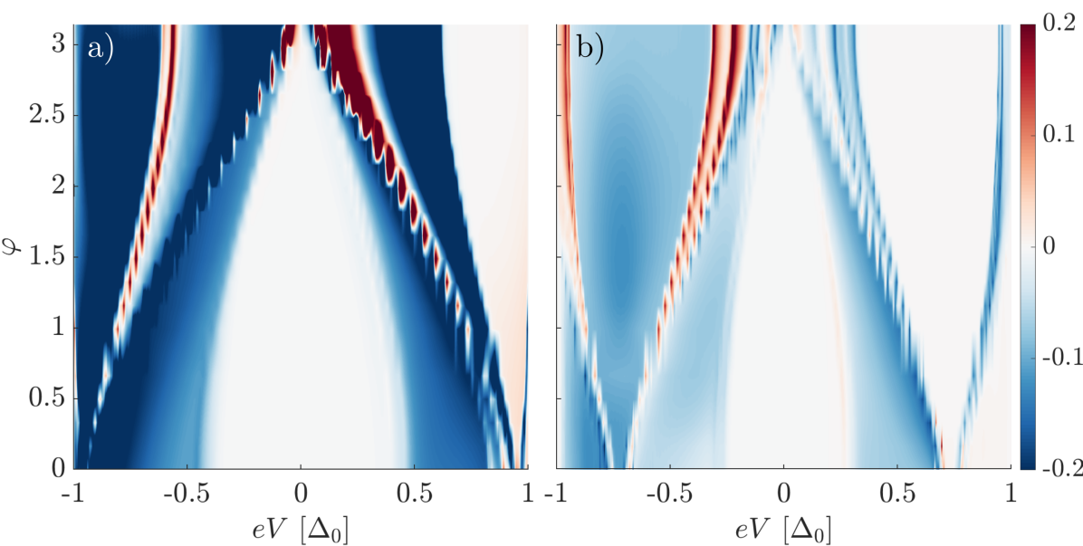
As mentioned previously, the superconducting phase difference can be another way to tune the non-local transport. Typically, the Josephson junction where should be tuned is part of a large SQUID loop [50, 51]. The magnetic field used in e.g., Ref. [50] to change was of the order of mT. Such low magnetic fields should have negligible orbital effects in the top and bottom graphene layers, therefore we do not include it explicitly, i.e., through a vector potential , in the following calculations. We assume that the only relevant effect of the magnetic field is to change in the Josephson junction.
We discuss the dependence of the differential conductance in the calculations shown in Fig. 8(a), where we used the same as in Fig. 6(a), whereas Fig. 8(b) corresponds to the case in Fig. 7(a). We remind that as increases from to , the induced gap in the graphene layers is gradually reduced and goes to zero for , see Figs. 2(d)-(f). This appears as a shrinking, low-conductance white region for in Fig. 8(a) and 8(b). However, is finite and negative in the range for most values of , suggesting that CAR is also robust to the change of . Similar behavior can be seen for both and . We have checked that for symmetric doping the differential conductance is mostly positive for all values of , i.e., the interlayer transport is dominated by EC.
V Conclusion
In conclusion, we have studied non-local Andreev reflection in a monolayer graphene based double JJ geometry. We have shown, that the ABSs appearing in the graphene layers hybridize and form AMSs. By studying the non-local differential conductance, we found that choosing an asymmetric doping profile in the graphene layers leads to CAR dominated transport mediated by the AMSs. Changing the doping profile to a symmetric one leads to the suppression of CAR. Importantly, the observed negative differential conductance does not require a very low doping of the graphene layers, which is difficult to achieve. We found that the negative non-local differential conduction is robust with respect to the junction length, changes in the doping of the graphene layers and the superconducting phase difference.
VI Acknowledgments
This work was supported by the ÚNKP-22-5 New National Excellence Program of the Ministry for Innovation and Technology from the source of the National Research, Development and Innovation Fund and by the Hungarian Scientific Research Fund (OTKA) Grant No. K134437. A.K. and P. R. acknowledge support from the Hungarian Academy of Sciences through the Bólyai János Stipendium (BO/00603/20/11 and BO/00571/22/11) as well. The research was supported by the Ministry of Innovation and Technology and the National Research, Development and Innovation Office within the Quantum Information National Laboratory of Hungary and we acknowledge the computational resources provided by the Wigner Scientific Computational Laboratory (WSCLAB).
References
- Vidal [2003] G. Vidal, Efficient classical simulation of slightly entangled quantum computations, Phys. Rev. Lett. 91, 147902 (2003).
- Recher et al. [2001] P. Recher, E. V. Sukhorukov, and D. Loss, Andreev tunneling, Coulomb blockade, and resonant transport of nonlocal spin-entangled electrons, Phys. Rev. B 63, 165314 (2001).
- Lesovik et al. [2001] G. Lesovik, T. Martin, and G. Blatter, Electronic entanglement in the vicinity of a superconductor, Eur. Phys. J. B 24, 287–290 (2001).
- Samuelsson et al. [2003] P. Samuelsson, E. V. Sukhorukov, and M. Büttiker, Orbital entanglement and violation of bell inequalities in mesoscopic conductors, Phys. Rev. Lett. 91, 157002 (2003).
- Prada and Sols [2004] E. Prada and F. Sols, Entangled electron current through finite size normal-superconductor tunneling structures, The European Physical Journal B - Condensed Matter and Complex Systems 40, 379 (2004).
- Beckmann et al. [2004] D. Beckmann, H. B. Weber, and H. v. Löhneysen, Evidence for crossed Andreev reflection in superconductor-ferromagnet hybrid structures, Phys. Rev. Lett. 93, 197003 (2004).
- Russo et al. [2005] S. Russo, M. Kroug, T. M. Klapwijk, and A. F. Morpurgo, Experimental observation of bias-dependent nonlocal Andreev reflection, Phys. Rev. Lett. 95, 027002 (2005).
- Hofstetter et al. [2009] L. Hofstetter, S. Csonka, J. Nygård, and C. Schönenberger, Cooper pair splitter realized in a two-quantum-dot Y-junction, Nature 461, 960 (2009).
- Hofstetter et al. [2011] L. Hofstetter, S. Csonka, A. Baumgartner, G. Fülöp, S. d’Hollosy, J. Nygård, and C. Schönenberger, Finite-bias Cooper pair splitting, Phys. Rev. Lett. 107, 136801 (2011).
- Das et al. [2012] A. Das, Y. Ronen, M. Heiblum, D. Mahalu, A. V. Kretinin, and H. Shtrikman, High-efficiency Cooper pair splitting demonstrated by two-particle conductance resonance and positive noise cross-correlation, Nat. Commun. 3, 1165 (2012).
- Ueda et al. [2019] K. Ueda, S. Matsuo, H. Kamata, S. Baba, Y. Sato, Y. Takeshige, K. Li, S. Jeppesen, L. Samuelson, H. Xu, and S. Tarucha, Dominant nonlocal superconducting proximity effect due to electron-electron interaction in a ballistic double nanowire, Science Advances 5, eaaw2194 (2019).
- Kürtössy et al. [2022] O. Kürtössy, Z. Scherübl, G. Fülöp, I. E. Lukács, T. Kanne, J. Nygård, P. Makk, and S. Csonka, Parallel inas nanowires for cooper pair splitters with coulomb repulsion 10.48550/arXiv.2203.14397 (2022).
- Wang et al. [2022] G. Wang, T. Dvir, G. P. Mazur, C.-X. Liu, N. van Loo, S. L. D. t. Haaf, A. Bordin, S. Gazibegovic, G. Badawy, E. P. A. M. Bakkers, M. Wimmer, and L. P. Kouwenhoven, Singlet and triplet Cooper pair splitting in superconducting-semiconducting hybrid nanowires (2022).
- Herrmann et al. [2010] L. G. Herrmann, F. Portier, P. Roche, A. L. Yeyati, T. Kontos, and C. Strunk, Carbon nanotubes as Cooper-pair beam splitters, Phys. Rev. Lett. 104, 026801 (2010).
- Schindele et al. [2012] J. Schindele, A. Baumgartner, and C. Schönenberger, Near-unity Cooper pair splitting efficiency, Phys. Rev. Lett. 109, 157002 (2012).
- Brange et al. [2021] F. Brange, K. Prech, and C. Flindt, Dynamic Cooper pair splitter, Phys. Rev. Lett. 127 (2021).
- Tan et al. [2015] Z. B. Tan, D. Cox, T. Nieminen, P. Lähteenmäki, D. Golubev, G. B. Lesovik, and P. J. Hakonen, Cooper pair splitting by means of graphene quantum dots, Phys. Rev. Lett. 114, 096602 (2015).
- Borzenets et al. [2015] I. Borzenets, Y. Shimazaki, G. Jones, M. Craciun, S. Russo, Y. Yamamoto, and S. Tarucha, High efficiency CVD graphene-lead (Pb) Cooper pair splitter, Scientific Rep. 6 (2015).
- Pöschl et al. [2022] A. Pöschl, A. Danilenko, D. Sabonis, K. Kristjuhan, T. Lindemann, C. Thomas, M. J. Manfra, and C. M. Marcus, Nonlocal conductance spectroscopy of Andreev bound states in gate-defined InAs/Al nanowires 10.48550/arXiv.2204.02430 (2022).
- Falci et al. [2001] G. Falci, D. Feinberg, and F. W. Hekking, Correlated tunneling into a superconductor in a multiprobe hybrid structure, Europhys. Lett. 54, 255 (2001).
- Walldorf et al. [2020] N. Walldorf, F. Brange, C. Padurariu, and C. Flindt, Noise and full counting statistics of a Cooper pair splitter, Phys. Rev. B 101, 205422 (2020).
- Liu et al. [2022] C.-X. Liu, G. Wang, T. Dvir, and M. Wimmer, Tunable superconducting coupling of quantum dots via Andreev bound states (2022).
- Cayssol [2008] J. Cayssol, Crossed Andreev reflection in a graphene bipolar transistor, Phys. Rev. Lett. 100, 147001 (2008).
- Veldhorst and Brinkman [2010] M. Veldhorst and A. Brinkman, Nonlocal cooper pair splitting in a junction, Phys. Rev. Lett. 105, 107002 (2010).
- Xue et al. [2011] J. Xue, J. Sanchez-Yamagishi, D. Bulmash, P. Jacquod, A. Deshpande, K. Watanabe, T. Taniguchi, P. Jarillo-Herrero, and B. J. LeRoy, Scanning tunnelling microscopy and spectroscopy of ultra-flat graphene on hexagonal boron nitride, Nat. Mat. 10, 282 (2011).
- Mayorov et al. [2012] A. S. Mayorov, D. C. Elias, I. S. Mukhin, S. V. Morozov, L. A. Ponomarenko, K. S. Novoselov, A. K. Geim, and R. V. Gorbachev, How close can one approach the Dirac point in graphene experimentally?, Nano Lett. 12, 4629 (2012).
- Park et al. [2019] G.-H. Park, K. Watanabe, T. Taniguchi, G.-H. Lee, and H.-J. Lee, Engineering crossed Andreev reflection in double-bilayer graphene, Nano Lett. 19, 9002 (2019).
- Efetov et al. [2016] D. K. Efetov, L. Wang, C. Handschin, K. B. Efetov, J. Shuang, R. Cava, T. Taniguchi, K. Watanabe, J. Hone, C. R. Dean, and P. Kim, Specular interband Andreev reflections at van der Waals interfaces between graphene and NbSe2, Nat. Phys. 12, 328 (2016).
- Pandey et al. [2021] P. Pandey, R. Danneau, and D. Beckmann, Ballistic graphene Cooper pair splitter, Phys. Rev. Lett. 126, 147701 (2021).
- Soori and Mukerjee [2017] A. Soori and S. Mukerjee, Enhancement of crossed andreev reflection in a superconducting ladder connected to normal metal leads, Phys. Rev. B 95, 104517 (2017).
- Nehra et al. [2019] R. Nehra, D. S. Bhakuni, A. Sharma, and A. Soori, Enhancement of crossed andreev reflection in a kitaev ladder connected to normal metal leads, Journal of Physics: Condensed Matter 31, 345304 (2019).
- Pillet et al. [2019] J.-D. Pillet, V. Benzoni, J. Griesmar, J.-L. Smirr, and . C. O. Girit, Nonlocal Josephson effect in Andreev molecules, Nano Letters 19, 7138 (2019).
- Kornich et al. [2019] V. Kornich, H. S. Barakov, and Y. V. Nazarov, Fine energy splitting of overlapping Andreev bound states in multiterminal superconducting nanostructures, Phys. Rev. Res. 1, 033004 (2019).
- Indolese et al. [2020] D. I. Indolese, P. Karnatak, A. Kononov, R. Delagrange, R. Haller, L. Wang, P. Makk, K. Watanabe, T. Taniguchi, and C. Schönenberger, Compact SQUID realized in a double-layer graphene heterostructure, Nano Letters 20, 7129 (2020).
- Bretheau et al. [2017] L. Bretheau, J. I.-J. Wang, R. Pisoni, K. Watanabe, T. Taniguchi, and P. Jarillo-Herrero, Tunnelling spectroscopy of Andreev states in graphene, Nature Physics 13, 756 (2017).
- Titov and Beenakker [2006a] M. Titov and C. W. Beenakker, Josephson effect in ballistic graphene, Phys. Rev. B 74, 041401(R) (2006a).
- Tworzydło et al. [2006] J. Tworzydło, B. Trauzettel, M. Titov, A. Rycerz, and C. W. J. Beenakker, Sub-poissonian shot noise in graphene, Phys. Rev. Lett. 96, 246802 (2006).
- Titov and Beenakker [2006b] M. Titov and C. W. J. Beenakker, Josephson effect in ballistic graphene, Phys. Rev. B 74, 041401 (2006b).
- [39] Eötvös quantum utilities, http://eqt.elte.hu/EQuUs/html/.
- Titov et al. [2007] M. Titov, A. Ossipov, and C. W. Beenakker, Excitation gap of a graphene channel with superconducting boundaries, Phys. Rev. B 75, 045417 (2007).
- Manjarrés et al. [2014] D. A. Manjarrés, S. Gomez P., and W. J. Herrera, Andreev levels in a Andreev superconductor graphene superconductor nanostructure, Physica B: Cond. Matt. 455, 26 (2014).
- Ben Shalom et al. [2016] M. Ben Shalom, M. J. Zhu, V. I. Fal’ko, A. Mishchenko, A. V. Kretinin, K. S. Novoselov, C. R. Woods, K. Watanabe, T. Taniguchi, A. K. Geim, and J. R. Prance, Quantum oscillations of the critical current and high-field superconducting proximity in ballistic graphene, Nat. Phys. 12, 318 (2016).
- Banszerus et al. [2020] L. Banszerus, F. Libisch, A. Ceruti, S. Blien, K. Watanabe, T. Taniguchi, A. K. Hüttel, B. Beschoten, F. Hassler, and C. Stampfer, Minigap and Andreev bound states in ballistic graphene arXiv:2011.11471 (2020).
- Cresti et al. [2003] A. Cresti, R. Farchioni, G. Grosso, and G. P. Parravicini, Keldysh-Green function formalism for current profiles in mesoscopic systems, Phys. Rev. B 68, 075306 (2003).
- Do [2014] V. N. Do, Non-equilibrium Green function method: theory and application in simulation of nanometer electronic devices, Advances in Natural Sciences: Nanoscience and Nanotechnology 5, 033001 (2014).
- Pala et al. [2008] M. G. Pala, M. Governale, and J. König, Nonequilibrium Josephson and Andreev current through interacting quantum dots, New Journal of Physics 10, 099801 (2008).
- Bolech and Giamarchi [2005] C. J. Bolech and T. Giamarchi, Keldysh study of point-contact tunneling between superconductors, Phys. Rev. B 71, 024517 (2005).
- Wu and Yip [2004] S.-T. Wu and S. Yip, ac Josephson effect in asymmetric superconducting quantum point contacts, Phys. Rev. B 70, 104511 (2004).
- Claughton et al. [1995] N. R. Claughton, M. Leadbeater, and C. J. Lambert, Theory of Andreev resonances in quantum dots, Journal of Physics: Condensed Matter 7, 8757 (1995).
- Nanda et al. [2017] G. Nanda, J. L. Aguilera-Servin, P. Rakyta, A. Kormá nyos, R. Kleiner, D. Koelle, K. Watanabe, T. Taniguchi, L. M. K. Vandersypen, and S. Goswami, Current-phase relation of ballistic graphene Josephson junctions, Nano Letters 17, 3396 (2017).
- Della Rocca et al. [2007] M. L. Della Rocca, M. Chauvin, B. Huard, H. Pothier, D. Esteve, and C. Urbina, Measurement of the current-phase relation of superconducting atomic contacts, Phys. Rev. Lett. 99, 127005 (2007).