Reversal of nanomagnets by propagating magnons in ferrimagnetic yttrium iron garnet enabling nonvolatile magnon memory
Abstract
Despite the unprecedented downscaling of CMOS integrated circuits, memory-intensive machine learning and artificial intelligence applications are limited by data conversion between memory and processor. There is a challenging quest for novel approaches to overcome this so-called von Neumann bottleneck. Magnons are the quanta of spin waves and transport angular momenta through magnets. They enable power-efficient computation without charge flow and would solve the conversion problem if spin wave amplitudes could be stored directly in a magnetic memory cell. Here, we report the reversal of ferromagnetic nanostripes by spin waves which propagate through an underlying spin-wave bus made from yttrium iron garnet. Thereby, the charge-free angular momentum flow is stored after transmission over a macroscopic distance. We show that spin waves can reverse large arrays of ferromagnetic stripes at a strikingly small power level of nW. Combined with the already existing wave logic, our discovery is path-breaking for the new era of magnonics-based in-memory computation and beyond von Neumann computer architectures.
Charge-based electronics exploiting semiconductors and metals have led to the digital age and given rise to ever increasing data-processing power during the last decades. The significant development slows down however due to overheating of processors at increased clock frequencies as well as the data-transfer bottleneck between charge-based processors and storage devices [1, 2]. So far, storage devices exploit reprogrammable states in materials classes which differ from the semiconductors and therefore require signal conversion. Waves for data processing like photons in optical computers already avoid, both, charge flow and the excessive Joule heating at high clock frequencies. However, even for optical computers the currently implemented von-Neumann device architecture still provokes the signal-conversion bottleneck, particularly in case of memory-intensive machine learning applications. Magnonics which is based on charge-free angular momentum flow via spin waves (magnons) promises to overcome the dilemmas. Making use of the bosonic quasiparticles [3], it offers low-power consuming wave-based computing with microwave signals up to THz frequencies [4, 5, 6]. A technology platform for disruptive information technologies is foreseen if the so far elusive nanomagnet switching by propagating spin waves would be experimentally demonstrated. This switching process in magnonic circuits would be path-breaking for both non-volatile storage of wave signals without conversion losses and in-memory computation [7, 8, 2]. Experiments presented in Ref. [9] are encouraging in that spin waves in an antiferromagnet excited by incoherent spin torques reversed an integrated micromagnet. However, such spin waves can not be used for wave logic. In Ref. [10], spin waves coherently excited in a magnon conduit by a microwave antenna induced the modification of magnetic domains. Here, the required power was however in the mW regime. We follow a different approach in that we excite spin waves in the ferrimagnetic insulator yttrium iron garnet (YIG) by radiofrequency (RF) signals and observe the magnon-induced reversal of ferromagnetic nanostripes integrated on its top surface (Fig. 1a). The shape anisotropy of the long and narrow permalloy (Py) stripes (green) allows for bistable magnetic states. Thereby, they represent magnetic bits with states ”0” and ”1”, and enable the nonvolatile storage of information (Fig. 1b, I and II). The underlying YIG (blue) allows us to transmit coherent magnons over macroscopic distances as their decay lengths in thin YIG are on the few 10 to 100 m length scale [11, 12]. They are far larger than electron scattering lengths in semiconductors and metals. We note that samples similar to the one shown in Fig. 1a have thoroughly been investigated recently in view of the so-called grating coupler effect. Different groups explored nanostripe arrays on YIG in their saturated states for the emission and detection of short-wave magnons [13, 14, 15, 16]. The magnon modes were transmitted over long distances [14] and imaged in real space by means of x-ray based magnetic microscopy [16]. However, the groups did not investigate if states of ferromagnetic nanostripes were different before and after spin-wave excitation at different power levels. Here, we report experiments that we performed on YIG spin-wave buses (delay lines) with integrated grating couplers (Fig. 1a) and led to the discovery of irreversible switching of the nanostripes by propagating magnons. By combining power-dependent spin-wave spectroscopy and magnetic force microscopy we evidence the storage of magnon signals in the YIG-based magnonic circuit containing ferromagnetic stripes. Importantly, the magnon-induced reversal reported here is induced by magnons which are transported over a macroscopic distance (m). This goes beyond Refs. [9, 17, 18, 19, 20] which considered distances on the nm length scale. Our finding is key for implementing data storage in wavelogic or neuromorphic computing architectures in magnonics [21]. Spin waves in YIG have already been shown to read out different magnetic states of integrated ferromagnetic stripes (Fig. 1b, III) [14, 22]. Combined with our discovery, in-memory computing and a complete read-and-write process of non-volatile magnetic bits via magnons in YIG circuits are now possible.
Reversal of ferromagnetic stripes on YIG observed by power-dependent spin-wave spectroscopy
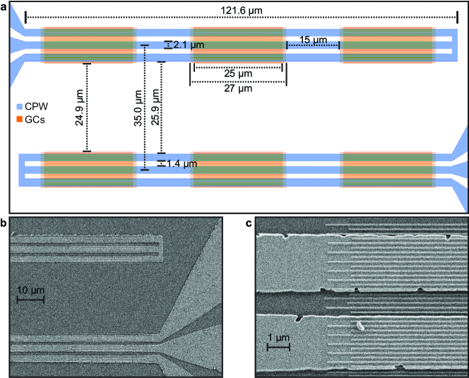
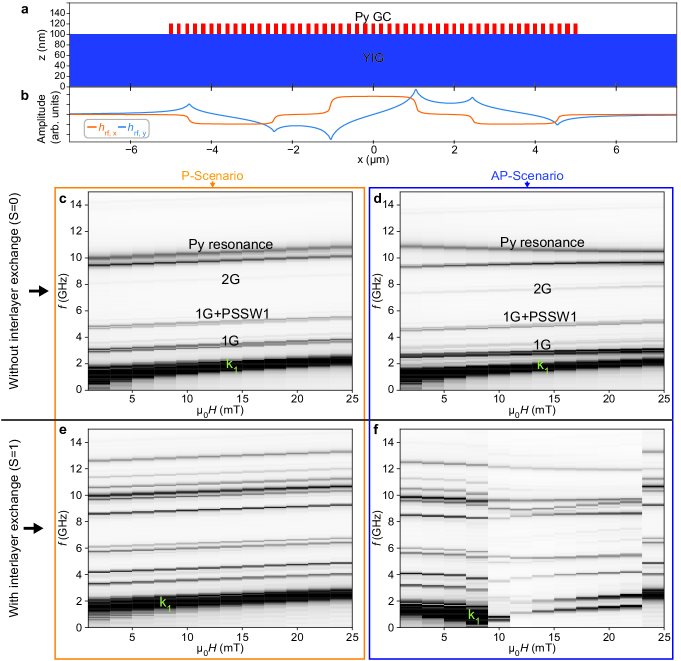
We studied different YIG-based magnonic circuits with integrated ferromagnetic nanostripes which showed magnon-induced reversal of nanomagnets reported here. We explored ferromagnetic nanostripes with widths between 50 and 200 nm, lengths up to 27 m, edge-to-edge separations down to 50 nm and different orientations with respect to spin-wave emitters. In this publication we focus on the magnonic circuit shown in Fig. 1a consisting of two nanostripe arrays which form grating couplers [23] on YIG underneath coplanar waveguides (CPWs). The insulating YIG with magnetization is 100 nm thick. The emitter (left) and detector (right) CPWs are connected to a vector network analyzer (VNA) which provides electromagnetic (em) waves at GHz frequencies at port 1. In such magnonic circuits information can be encoded in either the SW amplitudes or phases [24, 25, 4, 26].
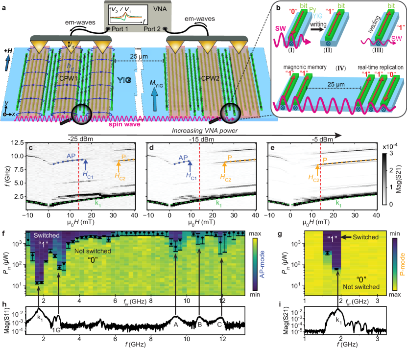
The magnetic component of the em wave, (field lines sketched in Fig. 1a), is converted into propagating spin-wave (SW) signals at the CPW via the torque , where is the gyromagnetic ratio and the vacuum permeability. We read out the SW signals both in reflection configuration at the emitter CPW1 and, after transmission through the YIG circuit, at the detector CPW2. The measured scattering parameters S11 and S21, respectively, are phase-resolved voltage signals induced by spin-precessional motion. The VNA offers a frequency resolution of 1 Hz and precisely adjusted power levels. In Fig. 1a, 25-m- and 27-m-long ferromagnetic nanostripes are integrated between CPWs and YIG (see Methods and Supplementary Fig. 1). These are bistable nanomagnets made from the ferromagnetic metal (permalloy, Py). In earlier works such bistable nanomagnets were investigated in the linear regime and gave rise to the grating coupler (GC) effect [23, 13, 14, 16]. Here, we report a nonlinear phenomenon in that GC stripes are reversed by spin waves which propagate through YIG. We show that thereby the storage of SW signals occur. To highlight the additional functionality of the ferromagnetic nanostripes we consider them to represent magnetic bits with either state ”0” (magnetization vector pointing along direction) or state ”1” ( along direction). Our findings hence demonstrate that propagating SWs in YIG can not only sense (”read”) the state of such magnetic bits (Fig. 1 b) as reported before [14, 22], but also reverse (”write”) magnetic states at appropriate power levels which can be still in the linear SW excitation regime.
The 100-nm-wide stripes considered here are arranged in separated periodic arrays with a common lattice constant nm. For the read-out (sensing) of ”0” and ”1” states we apply a small power level of only dBm at port 1 (or smaller) and make use of the GC effect in S11 and S21 spectra. It has already been shown that the signal strength and precise frequency of GC modes depended decisively on the field direction and relative magnetization directions of nanostripes and YIG [14, 15]. When the configuration of emitter and detector grating couplers were not symmetric the detection of emitted GC modes was not possible [27]. Using an in-plane magnetic field we reset the magnetic states of stripes to a well-defined initial state (”erase cycle”) before performing subsequent magnon-induced reversal experiments.
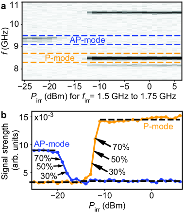
First, we show that the nanostripes in the magnonic circuit are switched from ”0” to ”1” by SWs exhibiting a certain amplitude. Figure 1 c-e displays the magnitude Mag(S21) of the frequency-dependent voltages at CPW2 as a function of field when measured for three different VNA power levels at CPW1. Dark branches indicate SW propagation. Initially, all nanostripes were magnetized along the direction (”erased”) by applying . Then was increased in 1 mT steps to the direction. For all powers , Mag(S21) contained a prominent and continuous low-frequency branch (marked by green dashed lines) attributed to the -mode of SWs excited by CPW1 directly in the YIG film [16]. The -branch changed slope close to , indicating that the magnetization of the soft magnetic YIG film was aligned with the external magnetic field for values of +1 mT and above. High frequency branches between roughly 7.5 and 12.5 GHz are attributed to the GC effect. They showed distinct transitions (jumps) in resonance frequencies. These frequency variations are known to indicate irreversible switching of Py nanostripes [14, 15]. Following Refs. [28, 29], the jumps occur at the switching fields at which the magnetization direction of nanostripes reverse. We focus on the two prominent branches marked by blue and orange dashed lines, which, in the following, we denote antiparallel (AP) and parallel (P) mode, respectively (Supplementary Methods). () defined the critical field value for which the signal strength of the AP-mode (P-mode) decreased (increased) to 50 % of its maximum value (see Methods and Supplementary Fig. 2). From Fig. 1 c to e, and diminished significantly with increasing indicating a nonlinear process and the reversal of nanostripes. Before presenting the magnon-induced reversal by means of frequency-resolved switching-yield maps introduced below, it is instructive to present magnetic force microscopy (MFM) data. We perform MFM at remanence to demonstrate that the magnon-induced reversal of ferromagnetic nanostripes is non-volatile.
Evidence of non-volatile state reversal after magnon transport in YIG
Figure 2 a displays an MFM image taken in the remnant configuration after we performed a broadband VNA measurement with dBm at mT on the sample with initially ”reset” magnetic stripes.
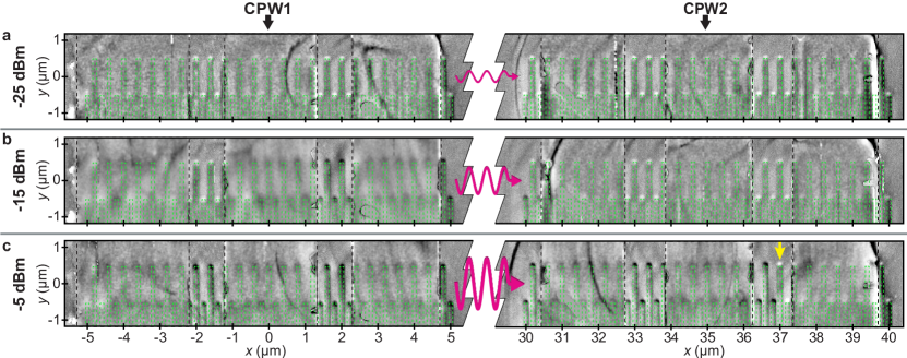
The MFM data show nanostripes at CPW1 and CPW2 which are magnetized still along direction and opposite to , consistent with our definition of the AP branch (cf. Fig. 1 c). Note that was intentionally below the evaluated onset field of quasistatistic reversal of magnetic stripes (Supplementary Fig. 3) in order to reveal SW-induced reversal processes. Figure 2 b shows the MFM data after applying an increased power level of dBm (31.6 ) at mT (cf. Fig. 1 d). The remnant MFM image shows nanostripes which on the right side of the signal line of CPW1 are reversed to the direction (state ”1”). On the left side with they are still magnetized along direction. Fallarino et al. [30] showed that SWs were excited nonreciprocally by a CPW for the same field geometry as used in our experiments. A large (small) SW amplitude was reported for the right (left) side of the signal line with (). We hence attribute the spatially inhomogeneous switching of nanostripes to the non-uniform (nonreciprocal) amplitude distribution of SWs excited in YIG. Stripes at CPW2 were still magnetized in direction for dBm, with the exception of the two stripes on the left edge. For this experiment with an intermediate power level, a large number of stripes of the two gratings was magnetized in opposite directions. This magnetic disorder explained the vanishingly small signal amplitude for GC modes in Fig. 1 d at 14 mT [27]. After a VNA measurement on again reset magnetic stripes with a high power of dBm (c.f. Fig. 1 e) the MFM data show that the majority of stripes below the emitter CPW1 was switched (Fig. 2 c). Below CPW2, about two thirds of the magnetic stripes were switched to ”1” as well. Only the stripes farthest away from CPW1 showed still the initial state ”0” (yellow arrow). The spatial variation agrees with a magnon-induced reversal process which requires a threshold amplitude of the SWs propagating under CPW2. As the amplitude of the propagating SWs decayed in positive -direction, the required amplitude was not available for a large propagation distance from CPW1. The MFM-detected magnetic states hence represent a non-volatile memory which records whether a certain threshold SW amplitude has locally been present (state ”1”) or not (state ”0”). Thereby, wave-based computational results can be stored without signal conversion. The reestablished magnetic order underneath both CPWs by high VNA power in Fig. 2 c explains the observation of the branch P at +14 mT in Fig. 1 e. We note that the significant asymmetry of switched nanostripes observed in Fig. 2 b and the subsequently presented experimental data allow us to exclude microwave-induced heating as the trigger for reversal. Heating in our continuous wave experiments would be most likely mirror-symmetric with respect to of the emitter CPW. The direct electromagnetic cross talk between CPW 1 and CPW2 is -50 dB (), i.e., vanishingly small.
Power-dependent reversal field reduction
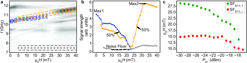
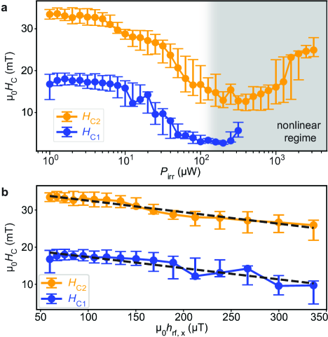
Figure 3 a summarizes how critical fields (blue line with dots) and (orange line with dots) extracted from VNA data depended on the power used in VNA spectroscopy. We find that () decreases from 16.8 mT (33.4 mT) at to 2.7 mT (12.9 mT) at . This corresponds to a reduction of by 84 % and by 61 %. Surprisingly, for large we find again an increase of and . We attribute this observation to the onset of nonlinear SW scattering (Supplementary Fig. 4), which limits the peak amplitude of SWs emitted from CPW1 [31]. For above -9 dBm (shaded with gray in Fig. 3 a) we found a red-shift of the -mode resonance frequency (Supplementary Fig. 4), which is an indication for nonlinear SW excitation [32]. The reoccurring increase of critical fields is counterintuitive if heating of Py nanostripes by high-power microwaves would be at the origin of the observed reversal phenomenon. If we plot and versus [33] (Fig. 3 b), the slopes (straight lines) show that a small in-plane RF field amplitude of only 0.35 mT provokes a critical field reduction by about 10 mT ( and m, see Supplementary figures). Hence, the RF-field-excited SWs in YIG reduce the stripes’ switching fields about times more efficiently than a static Oersted field applied oppositely to .
Magnon-induced reversal of magnetic nanostripes at low power level
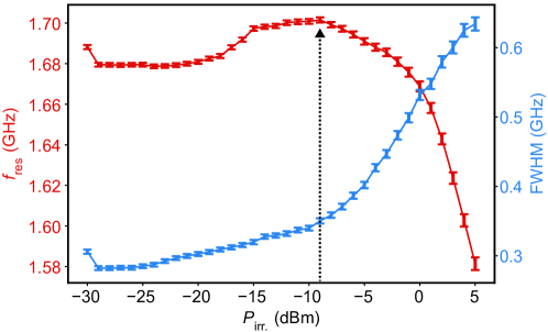
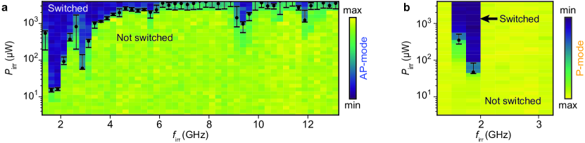
To evaluate quantitatively the critical powers needed to reverse ferromagnetic nanostripes (”switching-yield map”), we excited SWs at well-defined frequencies , varied the excitation power and explored after each power step whether the magnetic configuration of nanostripes changed (Supplementary Fig. 2). We defined () as the critical power value at which mode branches exhibited 50 % of their maximum signal strength, indicating that a considerable number of Py nanostripes under CPW1 (CPW2) were switched; the results for an applied field mT are summarized by black dots in Fig. 1 f (g) (datasets for a separate sample are shown in Supplementary Fig. 5). We considered further dBmmT and obtained consistent diagrams (not shown). We find the minimum of 12.6 W when applying an RF signal to CPW1 in the frequency window GHz to 1.75 GHz. This window includes the peak frequency of the -mode (1.70 GHz) with a wavelength of 7.4 m (Methods), as evidenced by the SW absorption spectrum Mag(S11) (Fig. 1 h). We note that this wavelength is much longer than both the width of stripes and the period of arrays. The wavelength is not commensurable with the stripe period . The second lowest of 68.9 W occurs for GHz to 3.0 GHz. This frequency range coincides with the frequency of the GC mode named . This mode exhibits a wavelength of 195 nm which is a value close to period (for mode identification see Supplementary Fig. 6 and Ref. [16] for the P-mode). The microwave power which is transferred into magnetization precession is evaluated by . We obtain critical power values and for magnetic stripe reversal by means of the mode and the short-wave magnon labelled , respectively. The switching-yield map features three further dips at high frequency marked as A, B, and C. They occur at relatively large power values of 0.69 mW, 1.91 mW and 1.13 mW for near 9.25 GHz, 10.75 GHz and 11.75 GHz, respectively. These dips agree with eigenresonances of the Py stripes. At such frequencies, the concomitant reversal of Py stripes underneath CPW1 is attributed to the conventional microwave-assisted magnetization reversal (MAMR). MAMR of individual nanomagnets was pioneered in 2003 [34] and then applied to mesoscopic Py magnets in e.g. Refs. [28, 29, 35, 33]. These micromagnets were not exposed to a propagating spin wave. Instead, they were irradiated directly by an RF signal. Its frequency hit exactly the eigenfrequency of the Py. We measured the direct electromagnetic crosstalk between the CPWs. At CPW2, it amounted to -50 dB. In other words, the directly irradiated microwave power was five (!) orders of magnitude lower and too small for MAMR at CPW2. The dips in Fig. 1f that occur near 8 GHz will not be discussed in the following. The important features are the ones at low frequency in Fig. 1f and g. They go beyond MAMR in that (1) we excite spin precession in YIG and not in the Py nanostripes, (2) different spin-wave frequencies in the YIG induce switching of Py nanostripes and (3), nanostripes more than 25 micrometres away from the emitter CPW reverse (Fig. 1g).
(Fig. 1g) is the critical power for magnetic stripe reversal under CPW2. We find W when exciting the -mode in YIG (Fig. 1 i). Its eigenfrequency was slightly blue-shifted compared to spectra taken for evidencing the concomitant magnetic stripe reversal by the -mode at CPW1. Hence, a SW mode near 2 GHz can ”write” states ”1” at CPW1 and perform a real-time replication of these bit-states ”1” about 25 m away [Fig. 1(b), panel IV]. Similar to Ref. [22] we observed that reversed stripes changed the transmitted SW amplitude. Such a signal variation was recently functionalized in a neuronal network based on propagating magnons [21]. The maximum distance over which reversal is possible is determined by the intermediate damping as will be discussed in the following.
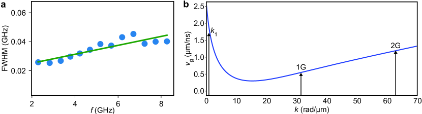
The minimum at CPW2 is about 4.5 times larger than the minimum . We attribute this discrepancy to the damping of the propagating SW mode. Assuming and a decay length of , the intensity of a SW would decay by 1/4.5 over a distance , i.e., the center-to-center distance between CPW1 and CPW2. Based on the intrinsic Gilbert damping of the YIG film, we calculate a decay length of for SWs with a wave vector in unpatterned YIG (Supplementary Fig. 7). It is reasonable to assume that the effective damping parameter in the magnonic circuit of Fig. 1 was larger due to additional magnon scattering and radiative losses [36]. We hence consider m to be a reasonable value. The mode has a smaller velocity than mode (Supplementary Fig. 7b) and thereby a further decreased decay length. This consideration explains why the maximum available power of the VNA was not sufficient for nanostripe reversal via mode underneath CPW2.
Discussion
The magnon-induced reversal of bistable ferromagnetic nanoelements via different propagating spin wave modes such as and in YIG is a key asset when aiming at in-memory computation and beyond von-Neumann device architectures based on multi-frequency magnonic circuits. Further studies are needed to understand the microscopic mechanism behind the magnon-induced reversal reported here and thereby predict the theoretical limit of minimum power consumption. But already at this stage several considerations can be made. CPWs and grating couplers emit spin waves at specifically designed wave vectors and due to the spin wave dispersion relation in YIG a specific frequency band is thereby realized. Importantly we observe low-power magnon-induced reversal for both a pure CPW mode (mode ) and a GC mode (). The nature of the mode does not seem to play a decisive role. The observed frequency selectivity is so far attributed to the microwave-to-magnon transducer used and not the reversal process itself. A decade ago, J. C. Slonczewski pointed out that magnons in a ferrimagnet/ferromagnet hybrid structure have the potential to provide spin-transfer torque for nanomagnet reversal more efficiently than charge flow [17]. His theoretical predictions reflected that for a given amount of energy more bosonic magnons than fermionic electrons could be generated. If transferred to an adjacent nanomagnet, each of these magnons provided an angular momentum of for reversal. Beyond this so-called magnon torque, spin precessional motion in YIG was found to inject a spin-polarized current into Py [37]. The spin current displayed a nonreciprocal behavior [38] and its amplitude increased with the SW wave vector in YIG [38, 39]. The spatial symmetry of our MFM data of reversed stripes is consistent with both the predicted magnon torque or . Furthermore, the and modes have indeed shown a characteristically different power level for reversal. One might hence speculate that magnon torque [10, 9, 19, 20] and/or spin current [18, 38] could play a role for the switching of Py stripes. We note however that we observe similar reversal also in hybrid structures with a 5 nm thick intermediate layer between YIG and Py consisting of either the insulator SiO2 or metal Cu [40]. These further experiments and results will be presented elsewhere, but render the so far discussed scenarios unlikely as their efficiency should vary significantly with the different intermediate layers. We speculate that the dipolar magnetic fields of propagating spin waves introduce torques on Py magnetic moments. As the frequencies of SW modes and in YIG are well below the eigenfrequencies of the Py nanostripes (Fig. 1f and g and Supplementary Fig. 5), they do not fulfill the condition for resonant chiral absorption discussed theoretically in Ref. [41]. A possible scenario might instead consist of SW-induced nucleation of a domain wall followed by its propagation due to the applied static magnetic field. We now compare the power levels reported here with the pioneering spin-transfer torque experiment in Ref. [42] performed in zero and non-zero applied fields . In Ref. [42], a directly injected electrical (el) current was used to switch one single Co nanomagnet of a small volume . A minimum power was required. In our study, we evaluated a critical power of when reversing a few 10 Py nanostripes of a much larger volume each. In our so-far non-optimized magnonic devices, the required power levels are also orders of magnitude below the ones recently reported for domain-wall manipulation by SWs in Py stripes and the torques produced by incoherent magnons in a thin antiferromagnetic barrier [10, 9]. Stimulated by Ref. [17], we argue that the bosonic nature of magnons is in general advantageous to initiate magnet reversal. In our experiments, the magnons in YIG had frequencies around 2 GHz. They were hence of low energy where is the Planck constant. Consequently, a small power can generate a large number of identical low-energy magnons in a short time which then produce torques for reversal via different scenarios outlined above. We expect further reduced critical power levels for magnetic bit reversal and smaller by optimizing microwave-to-magnon transducers, modifying the shape or volume of nanomagnets and engineering the interface between magnetic bit and magnon conduit via e.g. an antiferromagnetic layer.
Methods
Sample Fabrication
The samples were prepared on a 100 nm thick yttrium iron garnet (YIG) film, which was grown by liquid phase epitaxy and purchased from the Matesy GmbH in Jena, Germany. On top of the insulating YIG, a 20 nm thick metallic Py () film was deposited via electron beam evaporation. The grating pattern was defined via electron beam lithography (EBL) using negative hydrogen silsesquioxane resist and transferred into the Py film by ion beam etching. The etching time was optimized to ensure minimal overetching into the YIG film. Coplanar waveguides were prepared by EBL lift-off processing using a PMMA/MMA double layer positive resist and evaporation of Ti/Cu (5 nm/110 nm).
Spin wave spectroscopy with a vector network analyzer
SW spectroscopy measurements were conducted with a VNA (Keysight PNA N5222A) in a microwave probe station with integrated in-plane magnetic field control. The magnetic field was created by electromagnets and stabilized via a Hall-sensor controlled feedback loop. High-frequency coaxial cables with impedance and microwave probes were used to connect port 1 and port 2 of the VNA to CPW1 and CPW2, respectively. For all conducted measurements, microwave power (or ) was only applied to port 1, i.e. only the scattering parameters S11 and S21 were measured. The front panel jumpers of the PNA N5222A were adjusted at port 2 to provide increased forward (S21) dynamic range. For measurement of the microwave spectra at different power levels (cf. Fig. 1 c-e and raw data for Fig. 3) the frequency was scanned from 10 MHz to 12.5 GHz in 3.1 MHz steps. An IF bandwidth of 1 kHz was used. For the switching-yield measurements (cf. Fig. 1 f and g) was scanned in 2.5 MHz steps. An IF bandwidth of 1 kHz and a dwell time of 50 ms was used. The magnitudes of the reflection and transmission scattering parameters Mag(S11) and Mag(S21) were calculated as the square‐root of the sum of the respective squared real and squared imaginary parts, after removing nonmagnetic background signals, which did not depend on the applied external magnetic field. is the measure of the relative absorbed power and used to calculate the power transferred from the CPW into the spin-precessional (prec) motion in the magnonic circuit. The most prominent SW excitation of CPW1 occurred at a wave vector m-1 [16]. The wavelength of the corresponding mode in YIG amounted to about 7.4 m. The periodic array of Py nanostripes gave rise to a reciprocal lattice vector and enabled the excitation of short-wave magnons by the grating coupler effect [23]. Its wave vector amounted to m) m-1. The absorption spectrum Mag(S11) in Fig. 1 h showed a double peak structure for the resonant feature labelled with 1G. We attributed the smaller peak on the low-frequency side of 1G to a grating coupler mode with and the larger high-frequency peak to . The mode exhibited an absolute wave vector of . Its wavelength amounted to nm under the stripe array [16]. This value was close to due to . The GC mode corresponded to a wavelength of 206 nm under CPW1. Considering its larger absorption strength we assumed mode to induce mainly the reversal of nanostripes in the text.
Analysis of Switching Fields
To determine the power and frequency dependence of the discovered switching process, the following measurement routine was conducted: The stripes were first magnetized downwards with and then the field was increased slowly to a positive bias field of . This field value was below at -25 dBm, i.e., below the evaluated minimum field of the switching field distribution (Supplementary Fig. 3). We monitored Mag(S21) with a low sensing power dBm. This power level was chosen such that itself was insufficient to induce switching. While staying at mT, we applied in a small frequency window with a range of 0.25 GHz. was increased from -30 dBm to 6 dBm in 1 dBm steps. After each power step, Mag(S21) was measured with in a frequency window from 7.5 GHz to 12.5 GHz. Thereby we covered the branches indicating the magnetic configuration of the stripes. After each such sequence the sample was reset to the initial state (bits were erased) for the next frequency . Supplementary Fig. 2a shows exemplarily Mag(S21) measured as a function of with . With increasing the AP-mode vanishes and the P-mode appears. We evaluate mode strengths as a function of (Supplementary Fig. 2b) by integrating Mag(S21) in the vicinity of the AP-mode (enclosed by blue dashed lines) and P-mode (enclosed by orange dashed lines). We define () as the critical power value for which the signal strength of the AP-mode (P-mode) is at 50 % of its maximum value (Supplementary Fig. 2b), indicating that 50 % of the Py nanostripes in the grating under CPW1 (CPW2) were switched. Further we extract the values for which 30 % and 70 % of the signal strength are reached as a measure of the switching power distribution (error bar). The measurements were repeated for different altered from 1 GHz to 13.25 GHz in 0.25 GHz wide windows. We quantified the relative numbers of reversed nanostripes by integrating the signal strengths in Mag(S21) spectra in the vicinity of the AP- and the P-mode (Methods). At the low power level of dBm we analyzed the quasistatic switching field (SF) distribution of Py nanostripes under CPW1 (Supplementary Fig. 3a and b) and found a full width half maximum of roughly 13 mT centered around a switching field value of mT (Supplementary Fig. 3c). With increasing we observed a decrease in SF values and a narrower distribution (Supplementary Fig. 3c) consistent with the writing of bits reported in the manuscript.
Acknowledgments
The authors acknowledge discussions with Andrea Mucchietto, Shreyas Joglekar, Michal Mruczkiewicz, and Anna Fontcuberta i Morral.
Funding
The research was supported by the SNSF via grant number 163016.
Author contributions
D.G. and K.B. planned the experiments and designed the samples. K.B. prepared the samples and performed the experiments. K.B. and D.G. analyzed and interpreted the data. K.B. and D.G. wrote the manuscript.
Competing interests
The authors declare that they have no competing interests.
Data availability
The datasets generated and/or analysed during the current study are available from the corresponding author on reasonable request.
Additional information
Supplementary Information is available for this paper.
Correspondence and requests for materials should be addressed to D.G. (email: dirk.grundler@epfl.ch).
Reprints and permissions information is available at www.nature.com/reprints.
References
- [1] Manipatruni, S., Nikonov, D. & Young, I. Beyond CMOS computing with spin and polarization. Nat. Phys. 14, 338–343 (2018).
- [2] Sebastian, A., Gallo, M. L., Khaddam-Aljameh, R. & Eleftheriou, E. Memory devices and applications for in-memory computing. Nat. Nanotechn. 15, 529–544 (2020).
- [3] Demokritov, S. et al. Bose–Einstein condensation of quasi-equilibrium magnons at room temperature under pumping. Nature 443, 430 (2006).
- [4] Khitun, A., Bao, M. & Wang, K. L. Magnonic logic circuits. J. Phys. D: Appl. Phys. 43, 264005 (2010). URL https://doi.org/10.1088%2F0022-3727%2F43%2F26%2F264005.
- [5] Chumak, A., Serga, A. & Hillebrands, B. Magnon transistor for all-magnon data processing. Nat. Commun. 5, 4700 (2014).
- [6] Mahmoud, A. et al. Introduction to spin wave computing. J. Appl. Phys. 128, 161101 (2020). URL https://doi.org/10.1063/5.0019328. eprint https://doi.org/10.1063/5.0019328.
- [7] International roadmap for devices and systems (IRDS). Tech. Rep. (2020). eprint https://irds.ieee.org/editions/2020.
- [8] Islam, R. et al. Device and materials requirements for neuromorphic computing. J. Phys. D: Appl. Phys. 52, 113001 (2019). URL https://doi.org/10.1088%2F1361-6463%2Faaf784.
- [9] Wang, Y. et al. Magnetization switching by magnon-mediated spin torque through an antiferromagnetic insulator. Science 366, 1125–1128 (2019).
- [10] Han, J., Zhang, P., Hou, J. T., Siddiqui, S. A. & Liu, L. Mutual control of coherent spin waves and magnetic domain walls in a magnonic device. Science 366, 1121–1125 (2019). URL https://science.sciencemag.org/content/366/6469/1121. eprint https://science.sciencemag.org/content/366/6469/1121.full.pdf.
- [11] Yu, H. et al. Magnetic thin-film insulator with ultra-low spin wave damping for coherent nanomagnonics. Sci. Rep. 4, 6848 (2014).
- [12] Maendl, S. & Grundler, D. Spin waves with large decay length and few 100 nm wavelengths in thin yttrium iron garnet grown at the wafer scale. Appl. Phys. Lett. 111, 012403 (2017). URL https://doi.org/10.1063/1.4991520. eprint https://doi.org/10.1063/1.4991520.
- [13] Yu, H. et al. Approaching soft X-ray wavelengths in nanomagnet-based microwave technology. Nat. Commun. 7, 11255 (2016).
- [14] Liu, C. et al. Long-distance propagation of short-wavelength spin waves. Nat. Commun. 9, 738 (2018).
- [15] Chen, J. et al. Excitation of unidirectional exchange spin waves by a nanoscale magnetic grating. Phys. Rev. B 100, 104427 (2019). URL https://link.aps.org/doi/10.1103/PhysRevB.100.104427.
- [16] Baumgaertl, K. et al. Nanoimaging of ultrashort magnon emission by ferromagnetic grating couplers at GHz frequencies. Nano Lett. 20, 7281–7286 (2020). URL https://doi.org/10.1021/acs.nanolett.0c02645. PMID: 32830984, eprint https://doi.org/10.1021/acs.nanolett.0c02645.
- [17] Slonczewski, J. C. Initiation of spin-transfer torque by thermal transport from magnons. Phys. Rev. B 82, 054403 (2010). URL https://link.aps.org/doi/10.1103/PhysRevB.82.054403.
- [18] Suresh, A., Bajpai, U., Petrović, M. D., Yang, H. & Nikolić, B. K. Magnon- versus electron-mediated spin-transfer torque exerted by spin current across an antiferromagnetic insulator to switch the magnetization of an adjacent ferromagnetic metal. Phys. Rev. Applied 15, 034089 (2021). URL https://link.aps.org/doi/10.1103/PhysRevApplied.15.034089.
- [19] Guo, C. Y. et al. Switching the perpendicular magnetization of a magnetic insulator by magnon transfer torque. Phys. Rev. B 104, 094412 (2021). URL https://link.aps.org/doi/10.1103/PhysRevB.104.094412.
- [20] Zheng, D. et al. High-efficiency magnon-mediated magnetization switching in all-oxide heterostructures with perpendicular magnetic anisotropy. Advanced Materials n/a, 2203038. URL https://onlinelibrary.wiley.com/doi/abs/10.1002/adma.202203038. eprint https://onlinelibrary.wiley.com/doi/pdf/10.1002/adma.202203038.
- [21] Papp, Á., Porod, W. & Csaba, G. Nanoscale neural network using non-linear spin-wave interference. Nat. Commun. 12, 6422 (2021).
- [22] Qin, H., Holländer, R. & Flajšman, et al.., L. Nanoscale magnonic Fabry-Pérot resonator for low-loss spin-wave manipulation. Nat. Commun. 12, 2293 (2021).
- [23] Yu, H. et al. Omnidirectional spin-wave nanograting coupler. Nat. Commun. 4, 2702 (2013).
- [24] Kostylev, M. P., Serga, A. A., Schneider, T., Leven, B. & Hillebrands, B. Spin-wave logical gates. Appl. Phys. Lett. 87, 153501 (2005).
- [25] Schneider, T. et al. Realization of spin-wave logic gates. Appl. Phys. Lett. 92, 022505 (2008).
- [26] Csaba, G., Papp, Á. & Porod, W. Perspectives of using spin waves for computing and signal processing. Phys. Lett. A 381, 1471–1476 (2017).
- [27] Maendl, S. & Grundler, D. Multi-directional emission and detection of spin waves propagating in yttrium iron garnet with wavelengths down to about 100 nm. Appl. Phys. Lett. 112, 192410 (2018). URL https://doi.org/10.1063/1.5026060. eprint https://doi.org/10.1063/1.5026060.
- [28] Nozaki, Y. et al. Microwave-assisted magnetization reversal in 0.36-m-wide permalloy wires. Appl. Phys. Lett. 91, 122505 (2007).
- [29] Topp, J., Heitmann, D. & Grundler, D. Interaction effects on microwave-assisted switching of Ni80Fe20 nanowires in densely packed arrays. Phys. Rev. B 80, 174421 (2009).
- [30] Fallarino, L. et al. Propagation of spin waves excited in a permalloy film by a finite-ground coplanar waveguide: A combined phase-sensitive micro-focused Brillouin light scattering and micromagnetic study. IEEE Trans. Magn. 49, 1033–1036 (2013).
- [31] Schultheiss, H., Vogt, K. & Hillebrands, B. Direct observation of nonlinear four-magnon scattering in spin-wave microconduits. Phys. Rev. B 86, 054414 (2012). URL https://link.aps.org/doi/10.1103/PhysRevB.86.054414.
- [32] Olson, H. M., Krivosik, P., Srinivasan, K. & Patton, C. E. Ferromagnetic resonance saturation and second order suhl spin wave instability processes in thin permalloy films. J. Appl. Phys. 102, 023904 (2007). URL https://doi.org/10.1063/1.2756481. eprint https://doi.org/10.1063/1.2756481.
- [33] Podbielski, J., Heitmann, D. & Grundler, D. Microwave-assisted switching of microscopic rings: Correlation between nonlinear spin dynamics and critical microwave fields. Phys. Rev. Lett. 99, 207202 (2007). URL https://link.aps.org/doi/10.1103/PhysRevLett.99.207202.
- [34] Thirion, C., Wernsdorfer, W. & Mailly, D. Switching of magnetization by nonlinear resonance studied in single nanoparticles. Nat. Mater. 2, 524 (2003).
- [35] Nembach, H. T. et al. Microwave assisted switching in a Ni81Fe19 ellipsoid. Appl. Phys. Lett. 90, 062503 (2007). URL https://doi.org/10.1063/1.2450645. eprint https://doi.org/10.1063/1.2450645.
- [36] Schoen, M. A. W. et al. Ultra-low magnetic damping of a metallic ferromagnet. Nat. Phys. 12, 839–842 (2016).
- [37] Hyde, P. et al. Electrical detection of direct and alternating spin current injected from a ferromagnetic insulator into a ferromagnetic metal. Phys. Rev. B 89, 180404 (2014). URL https://link.aps.org/doi/10.1103/PhysRevB.89.180404.
- [38] Iguchi, R. et al. Spin pumping by nonreciprocal spin waves under local excitation. Appl. Phys. Lett. 102, 022406 (2013). URL https://doi.org/10.1063/1.4775685. eprint https://doi.org/10.1063/1.4775685.
- [39] Sandweg, C. W., Kajiwara, Y., Ando, K., Saitoh, E. & Hillebrands, B. Enhancement of the spin pumping efficiency by spin wave mode selection. Appl. Phys. Lett. 97, 252504 (2010). URL https://doi.org/10.1063/1.3528207. eprint https://doi.org/10.1063/1.3528207.
- [40] Mucchietto, A., Baumgaertl, K. & Grundler, D. unpublished.
- [41] Kruglyak, V. V. Chiral magnonic resonators: Rediscovering the basic magnetic chirality in magnonics. Appl. Phys. Lett. 119, 200502 (2021). URL https://doi.org/10.1063/5.0068820. eprint https://doi.org/10.1063/5.0068820.
- [42] Albert, F. J., Katine, J. A., Buhrman, R. A. & Ralph, D. C. Spin-polarized current switching of a Co thin film nanomagnet. Applied Physics Letters 77, 3809–3811 (2000). URL https://doi.org/10.1063/1.1330562. eprint https://doi.org/10.1063/1.1330562.
- [43] Vansteenkiste, A. et al. The design and verification of MuMax3. AIP Advances 4, 107133 (2014). eprint https://doi.org/10.1063/1.4899186.
- [44] Kumar, D. & Adeyeye, A. O. Techniques in micromagnetic simulation and analysis. J. Phys. D: Appl. Phys. 50, 343001 (2017).
- [45] Yu, H. et al. High propagating velocity of spin waves and temperature dependent damping in a CoFeB thin film. Appl. Phys. Lett. 100, 262412 (2012). eprint https://doi.org/10.1063/1.4731273.
- [46] Wang, H. L. et al. Scaling of Spin Hall Angle in 3d, 4d, and 5d Metals from /Metal Spin Pumping. Phys. Rev. Lett. 112, 197201 (2014).
- [47] Kalinikos, B. A. & Slavin, A. N. Theory of dipole-exchange spin wave spectrum for ferromagnetic films with mixed exchange boundary conditions. J. Phys. C: Solid St. Phys. 19, 7013–7033 (1986).
SUPPLEMENTARY INFORMATION