E. Magnano: ]Department of Physics, University of Johannesburg, PO Box 524, Auckland Park 2006, South Africa
Origin and Quantitative Description of the NESSIAS Effect at Si Nanostructures
Abstract
The electronic structure of low nanoscale (LNS) intrinsic silicon (i-Si) embedded in SiO2 vs. Si3N4 shifts away from vs. towards the vacuum level , as described by the Nanoscale Electronic Structure Shift Induced by Anions at Surfaces (NESSIAS). Here, we fully explain the NESSIAS based on the quantum chemical properties of the elements involved. Deriving an analytic parameter to predict the highest occupied molecular orbital energy of Si nanocrystals (NCs), we use various hybrid-DFT methods and NC sizes to verify the accuracy of . We report on first experimental data of Si nanowells (NWells) embedded in SiO2 vs. Si3N4 by X-ray absorption spectroscopy in total fluorescence yield mode (XAS-TFY) which are complemented by ultraviolet photoelectron spectroscopy (UPS), characterizing their conduction band and valence band edge energies and , respectively. Scanning the valence band sub-structure by UPS over NWell thickness, we derive an accurate estimate of shifted purely by spatial confinement, and thus the actual shift due to NESSIAS. For 1.9 nm thick NWells in SiO2 vs. Si3N4, we get offsets of eV and eV, demonstrating a type II homojunction in LNS i-Si. This p/n junction generated by the NESSIAS eliminates any deteriorating impact of impurity dopants, offering undoped ultrasmall Si electronic devices with much reduced physical gate lengths and CMOS-compatible materials.
I Introduction
Silicon (Si) nanowells (NWells) with a thickness of nm embedded in silicon dioxide (SiO2) vs. silicon nitride (Si3N4) show an electronic structure shift with respect to the vacuum energy level as measured by ultraviolet photoelectron spectroscopy (UPS) and X-ray absorption spectroscopy in total fluorescence yield mode (XAS-TFY) König et al. (2018, 2019, 2021). NWells embedded in SiO2 (Si3N4) get shifted to higher (lower) binding energies, that is, away from (towards to) . This Nanoscopic Electronic Structure Shift Induced by Anions at Surfaces (NESSIAS) effect is caused by quantum chemical properties of the anions forming the dielectric which surrounds the low nanoscale (LNS) Si. While the NESSIAS effect has been established in theory and experiment, its exact origin and quantitative description are still elusive. Here, we deliver a detailed quantum chemical explanation of the NESSIAS effect, complemented with its semi-quantitative description which serves to predict NESSIAS in LNS intrinsic Si (i-Si) for a variety of anions in embedding/coating dielectrics. To this end, we provide experimental evidence and details of the quantum-chemical concept which leads to the NESSIAS effect.
The NESSIAS effect induces a p/n junction on semiconductor nanostructures such as fins, nanowires (NWires), or nanocrystals (NCs) by enabling an electron flooding of the nanostructure when coated with SiO2 König et al. (2021), or a virtually complete electron drainage from the nanostructure when coated with Si3N4 König et al. (2018, 2019), introducing a high density of holes into the nanovolume by the latter process. This re-arrangement of charge carrier densities has far-reaching consequences for semiconductor devices in very large scale integration (VLSI), ultra-low power and cryo-electronics. Spatial fluctuations of dopant densities, out-diffusion and self-purification impose a size limit onto VLSI devices as evident from physical gate lengths hovering around 20 nm since ca. 2014 111It is interesting to note in this context that the VLSI technology nodes do not reflect the physical gate length. We have a planar MOSFET model shrunken to a size where it would perform as the fin-FET of the respective technology node Col (2016).. With thermal dopant ionization not required, junctions induced by the NESSIAS effect should remain fully functional down to extremely low temperatures as useful for peripheral electronics in qbit manipulation Ladd et al. (2010).
The detection of the NESSIAS in LNS i-Si requires an absolute assignment of energies to , combined with elaborate UPS and XAS-TFY measurements and refined data processing for improved signal-to-noise ratios König et al. (2018, 2019, 2021). To this end, the structures under investigation have to be in the range of the NESSIAS impact length. Many published DFT calculations Garcia-Castello et al. (2015); Jarolimek et al. (2017); Ossicini et al. (2020); Halilov et al. (2020) lack an energy assignment on an absolute scale. Possibly identical LNS i-Si NWell systems near the low end of the one-digit nm range embedded in different dielectrics pose a challenge in experiment. The common perception of Si3N4 as an inferior dielectric on grounds of interface defect density König et al. (2022) and its more complex technology as opposed to SiO2 Lee et al. (2012) are likely reasons for the literature on LNS Si embedded in or coated with Si3N4 being rather scarce. Indeed, standard Si3N4 has an interface defect density to LNS Si which exceeds values of SiO2/Si interfaces ca. 13-fold Thoan et al. (2011); Basaa et al. (2000); König et al. (2022), though refined preparation techniques for high-quality H-passivated Si3N4-coatings rival trap densities on SiO2/Si interfaces Jung et al. (2011). This complex situation may explain why the NESSIAS might have been overlooked in the past.
After introducing the methods used in Section II, we deliver a phenomenological and qualitative explanation of the NESSIAS effect in Section III.1, resorting to quantum chemical properties of involved chemical elements. In Section III.2, we derive a semi-quantitative analytic parameter of the NESSIAS effect to describe the energy of the highest occupied molecular orbital (HOMO) as a function of anion-specific quantum chemical properties combined with the charge of these main anions of the ligand groups attached to Si NCs. In Section III.3, we test with a variety of density functionals (DFs) and most anionic elements of the first and second row of the periodic table with respect to Si, subject to the availability of experimental quantum chemical data. Our discussion is complemented with synchrotron data in Section III.4. Since the electronic structure of NWells shifts as a function of quantum confinement (QC), it is essential to separate this phenomenon induced by a spatial limit from the NESSIAS brought about by the quantum-chemical nature of embedding dielectric vs. Si. To this end, we evaluate our results from synchrotron UPS measurements in Section III.4.1, revealing sub-structures of the valence band which serve to estimate the actual QC. This true QC is revealed by the shift of the valence band (VB) edge to higher binding energies as a sole function of NWell thickness, occurring in all samples irrespective of the embedding dielectric. We use this VB edge as a reference level to estimate the actual NESSIAS as per embedding dielectric in the QC regime. Next, we evaluate our experimental data of the VB and conduction band (CB) edges as measured by synchrotron XAS-TFY in Section III.4.2, establishing the link between bulk Si and SiO2 vs. Si3N4 as given by ultrathin Si NWells coated with the respective dielectric. Section IV delivers a conclusion.
II Methods
II.1 Sample Preparation
After determining the Deal-Gove parameters Deal and Grove (1965) for the furnace oxidation of silicon-on-insulator (SOI) samples, the SOI crystalline Si (c-Si) layers (p-type, 1 cm) on Si wafers with 145 nm buried SiO2 (BOx) were oxidized down to a thickness of 2.1 to 6.0 nm. The SiO2 was removed by etching in a buffered oxide etch (BOE; 1 wt-% HF buffered with NH4F), followed by a self-limiting oxidation in 68 wt-% HNO3 at 120 ∘C, yielding a 1.1 to 5.0 nm Si-NWell with 1.4 nm SiO2 capping. A lateral metal contact frame was processed on the front surface by photolithographical structuring, wet-chemical etching in BOE for opening the top SiO2 layer and thermal evaporation of 300 nm Al, followed by a lift-off in acetone. The Si reference samples were contacted directly on their front surface. NWell samples were coated with photo resist immediatley after NWell thickness measurements using Mueller matrix ellipsometry straight after processing to prevent oxidation in air. Resist was removed just prior to sample mounting at the beamline. Si reference samples consisted of (001)-Si wafer (Sb-doped -type, 0.01 cm) which were treated with a BOE immediately before sample mounting under a N2 gas flow with swift loading into the ultra-high vacuum (UHV) annealing chamber.
Si-NWells in Si3N4 were processed in analogy to the ones in SiO2, using the same SOI wafers as starting point. The SOI was thinned down to a remanent Si device layer which was 1 nm thicker than the final NWell thickness, accommodating for Si consumption during the growth of Si3N4. Next, the SiO2 capping is removed with BOE immediately before growing 3 nm of Si3N4 in an ammonia atmosphere by rapid thermal nitridation (RTN). Afterwards, 20 nm of Si3N4 and 80 nm of SiO2 were deposited by plasma enhanced chemical vapor deposition, followed by chemical mechanical polishing of the SiO2 layer. After an RCA clean Kern and Deckert (1978), the samples were bonded to a Si sample Kräuter et al. (1998) covered by SiO2 of ca. 1.5 nm thickness which was grown during RCA-SC2 step. The original Si substrate of the SOI samples was etched back using a cyclic deep reactive ion etching process based on passivation with C4F8 and etching with SF6. The BOx served as a stopping layer and was subsequently removed by a BOE immediately before growing 1 nm of Si3N4 by RTN in ammonia atmosphere. Contacts to the NWells were fabricated by photolithography, etching the Si3N4 with 1 wt-% hydrofluroric acid and deposition of 300 nm Al.
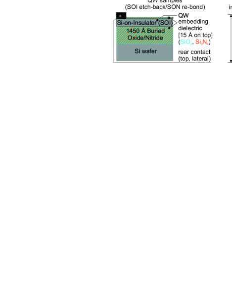
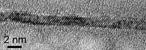
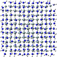
The layout of the samples and a high resolution TEM image of a NWell sample is shown Fig. 1.
(a)
(b)
II.2 Characterization
For synchrotron-based characterization techniques such as X-ray absorption spectroscopy measurements in total fluorescence yield (XAS-TFY) and UV photoelectron spectroscopy (UPS), all samples were subject to a UHV anneal for 60 min at 500 K to desorb water and air-related species from the sample surface prior to measurements. Synchrotron XAS-TFY measurements were carried out at the BACH CNR beamline Zangrando et al. (2004); Stebel et al. (2011) at the Elettra synchrotron radiation facility in Trieste, Italy, in top-up mode at an electron energy of 2.4 GeV (140 mA electron ring current). The photon energy scale has been calibrated using the energy position of the Si L3-edge (99.6 eV) measured on a reference (001)-Si wafer. A multitude of spectra was recorded per sample to obtain the data ensemble required for statistical post-processing. Further information and data on measurement parameters, measurement geometry, and statistical data post-processing can be found in Ref. Sup .
Synchrotron UPS measurements were realized at the BaDElPh beamline Petaccia et al. (2009) at the Elettra synchrotron radiation facility in Trieste, Italy, in top-up mode at an electron energy of 2.0 GeV (300 mA electron ring current). Single scans of spectra were recorded over 12 h per NWell sample and subsequently added up for eliminating white noise. Scans for the Si-reference sample were recorded over 2 h and subsequently added up. All NWell samples were excited with photon energies of initially 8.9 eV and of 8.0 eV for subsequent measurements, and a photon flux of ca. s-1. The incident angle of the UV beam onto the sample was 50∘ with respect to the sample surface normal, the excited electrons were collected with an electron analyzer along the normal vector of the sample surface. Energy calibration of the UPS was realized using a tantalum (Ta) stripe in electrical contact to the sample as work function reference. For details on UPS data and measurement, we refer to the supporting information of König et al. (2018) and the appendix of König et al. (2019).
The thickness of Si-NWells and its adjacent SiO2 layers were measured using an ACCURION nanofilm ep4se ellipsometer Acc (2020) using a Mueller matrix approach Mueller (1948); Azzam (1978); Savenkov (2009). Additional thickness measurements of the Si NWells and top SiO2 were carried out by Transmission Electron Microscopy (TEM) on selected samples to confirm and/or calibrate ellipsometry measurements, see to representative NWell image in Fig. 1(b). All TEM samples were capped with a protective 100 nm thick SiO2-layer to facilitate the preparation of X-sections by the focused ion beam (FIB) technique using a FEI Strata FIB 205 workstation. Some samples were further thinned by a Fischione NanoMill. TEM analysis of the X-sections was performed at a FEI Tecnai F20 TEM operated at 200 kV at the Central Facility for Electron Microscopy, RWTH Aachen University, and at the spherical aberration corrected FEI Titan 80-300 TEM operated at 300 kV at Ernst Ruska-Centre, Forschungszentrum Jülich Thust et al. (2016).
II.3 Density Functional Theory (DFT) Calculations
Real space calculations were carried out with a molecular orbital basis set (MO-BS) and Hartree-Fock (HF)/DFT methods, employing the Gaussian09 program package G09 (2012) with the GaussView program Dennington et al. (2009) for visualization. Initially, the MO-BS wavefunction ensemble was tested and optimized for describing the energy minimum of the system (variational principle; stable opt) with the HF method Hartree (1928a, b); Fock (1930). Exact exchange interaction inherent to HF is crucial in obtaining accurate bond geometries, see supporting information of König et al. (2018). As MO-BS, we used the Gaussian type 3-21G MO-BS Gordon et al. (1982). This HF/3-21G route was used for the structural optimization of approximants to obtain their most stable configuration (maximum integral over all bond energies); root mean square (RMS) and peak force convergence limits were 15.3 meV Å-1 and 23.1 meV Å-1, (300 and 450 Ha/), respectively. Optimized geometries were used to calculate their electronic structure by testing and optimizing the MO-BS wavefunction ensemble with the non-local hybrid DF B3LYP Becke (1988); Lee et al. (1988); Becke (1993), its modified form featuring the Coulomb Attenuation Method (CAM-B3LYP) for more accurate asymptotic non-local exchange interactions Yanai et al. (2004), and the HSE06 hybrid DF with its parameters from 2006 Krukau et al. (2006). As MO-BS, we used the Gaussian type 6-31G(d) MO-BS which contains d-polarization functions (B3LYP/6-31G(d) ) Francl et al. (1982) for all chemical elements. For all calculations, tight convergence criteria were set to the self-consistent field routine and no symmetry constraints to MOs were applied. Ultrafine integration grids were used throughout. The supporting information of König et al. (2014, 2018) contain detailed accuracy assessments.
III Results
III.1 Qualitative Explanation of the NESSIAS Effect
When a common boundary between two different solids with a bandgap is formed, an interface charge transfer (ICT) occurs Mönch (2001), generating an interface dipole which may shift the electron work function of both materials with respect to the intrinsic solid-vacuum interface Mönch (2001); Campbell et al. (1996). The solid which accumulates extrinsic electrons experiences an electronic structure shift to lower binding energies , hence to , the other solid which provides the electronic charge experiences an electronic structure shift in the opposite direction. When LNS i-Si is coated with 1 ML SiO2 or Si3N4, the ICT provides about the same amount of electrons to O and N as main interface anions in OH and NH2 groups König et al. (2019), see to top section in Table 1.
| approximant | ||||
|---|---|---|---|---|
| [nm] | [e] | [eV] | [eV] | |
| Si10(NH | ||||
| Si10(OH)16 | 0.72 | |||
| Si35(NH | ||||
| Si35(OH)36 | 1.10 | |||
| Si84(NH | ||||
| Si84(OH)64 | 1.48 | |||
| Si165(NH | ||||
| Si165(OH)100 | 1.85 | |||
| Si286(NH | ||||
| Si286(OH)144 | 2.22 | |||
| Si455(NH | ||||
| Si455(OH)196 | 2.59 | |||
| Si10 in 1.5 ML Si3N4 | ||||
| Si10 in 1.5 ML SiO2 | 0.72 | |||
| Si35 in 1.5 ML Si3N4 | ||||
| Si35 in 1.5 ML SiO2 | 1.10 | |||
| Si84 in 1.5 ML Si3N4 | ||||
| Si84 in 1.5 ML SiO2 | 1.48 | |||
| Si165 in 1.5 ML Si3N4 | ||||
| Si165 in 1.5 ML SiO2 | 1.85 | |||
| Si286 in 1.5 ML Si3N4 | ||||
| Si286 in 1.5 ML SiO2 | 2.22 |
We would thus expect a nearly identical shift of the LNS i-Si electronic structure in accord with interface dipole theory.
However, measurements of Si NCs König et al. (2014) and nanowells (NWells) König et al. (2018, 2019, 2021), and DFT calculations of Si NCs König et al. (2008, 2009, 2019) and nanowires (NWires) König et al. (2018) show a very different behavior. Energies of the lowest unoccupied MO (LUMO) , and listed in Table 1 show that Si NCs coated with SiO2 experience a shift to higher , and Si NCs coated in Si3N4 experience a shift to lower . This contradiction to interface dipole theory can be resolved when looking at the quantum chemical properties of the chemical elements involved. Such elements are LNS i-Si as the cation providing electrons, and in particular N or O as the anion receiving such electrons. Relevant properties of the anions are the electronegativity (EN) and resulting ionicity of bond (IOB) to Si, the ionization energy , the electron affinity for the neutral anion , and the electron affinity of the anion ionized with one electron , see Table 2. We focus on N and O as anions to explain the origin of the NESSIAS effect.
| element | EN∗ | IOB to Si | |||
|---|---|---|---|---|---|
| [%] | [eV] | [eV] | [eV] | ||
| Si | 1.74 | 0 | 8.15 | ||
| B | 2.01 | 2 | 8.30 | Scheer et al. (1998) | |
| H | 2.20 | 5 | 13.60 | Guo and Whitehead (1990) × | |
| C | 2.50 | 13 | 11.26 | Guo and Whitehead (1990) × | |
| N | 3.07 | 36 | 14.53 | Huheey (1983) | |
| O | 3.50 | 54 | 13.36 | Ginsberg and Miller (1958) × | |
| F | 4.10 | 75 | 17.42 | Guo and Whitehead (1990) × | |
| S | 2.44 | 12 | 10.36 | Guo and Whitehead (1990) × |
∗ Allred & Rochow † measured × calculated
Table 2 shows that N has a much more positive and still more positive than O, while its IOB to Si is ca. 2/3 of the value O provides. This lower IOB and thus the charge of the ICT per bond is nearly cancelled out by N in Si3N4 having 3/2 interface bonds to Si on average due to its trivalent configuration. Thus, values of the cumulative charge transferred to the main anions for NCs of same size embedded into 1 ML SiO2- vs. Si3N4 are nearly equal. The situation changes when the dielectric embedding increases from 1 to 1.5 ML König et al. (2019), see bottom section of Table 1. For 1.5 ML SiO2, increases for SiO2-embedding, though this increase drops from ca. 16 % for Si10 NCs to ca. 2 % for Si286 NCs. We also see a slight shift of towards at Si286 and Si455 NCs, and a shift of towards for Si455 NCs, indicating an ICT saturation for 1 ML SiO2, and thereby a saturation of NESSIAS at this NC size and embedding. Such saturation cannot be seen for an embedding in 1.5 ML SiO2. Looking at NCs embedded in 1 ML Si3N4, we see that has lower values when compared to the same NC in 1 ML SiO2, whereby the difference diminishes from ca. % for Si10 NCs to ca. % for Si455 NCs. There is no additional shift of and away from , strongly suggesting that the NESSIAS effect is not saturated with 1 ML Si3N4 for Si455 NCs. For 1.5 ML Si3N4-embedding, drops notably from a slight overshoot of ca. 2 % for Si10 NCs to % for a Si286 NC, dropping accordingly more when compared to Si NCs in 1.5 ML SiO2. Although is the lowest for 1.5 ML Si3N4-embedding, the values of and relative to remain virtually unchanged when compared to embedding in 1 ML Si3N4. We found the same result from DFT where two Si NCs ranging from 0.7 to 1.9 nm size (Si10 to Si165) were calculated within one approximant, one of which was embedded in SiO2, and the other in Si3N4, with 3 ML of dielectric between them König et al. (2018, 2019), see also Ref. Sup for details. We thus can state for SiO2-embedding that the NESSIAS effect is rather spatially compact and comes out of saturation fairly quickly with increasing LNS i-Si system size. For Si3N4-embedding, the NESSIAS effect is spatially distributed and the electronic shift is rather smooth, extending over a wider range of LNS i-Si system size. In order to understand this peculiar electronic structure, we look at a sketch combining spatial atomic orbital (AO) distribution and energy levels, see Fig. 2.
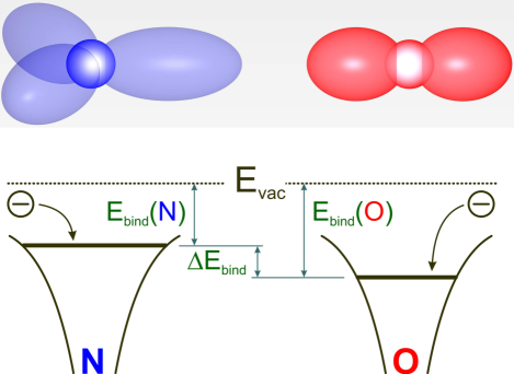
Arguably, the delocalizing impact of N vs. the localizing impact of O onto their acquired electronic charge is the key to the NESSIAS effect. We can interpret a decreased for N as a partial reflection of back into the LNS i-Si. These observations are supported by a decreasing per NC size when going from 1 to 1.5 ML Si3N4-embedding, being confirmed indirectly by experimental results of Si3N4- vs. SiO2-embedded Si NWells, see Section III.4.1 and Fig. 8. The atomistic nature of the NESSIAS implies a short impact length in accord with other near-field effects such as significant electron tunneling Brar et al. (1996). For LNS i-Si, the extension of the NESSIAS is ca. 1.3 to 1.8 nm per plane interface König et al. (2018, 2019, 2021).
III.2 Analytic Relation of the NESSIAS Effect with the HOMO Energy
We consider interfaces constituted by single bonds, such as between Si/SiO2 and Si/Si3N4. A detailed derivation of the equations below and the use , and of the interface main anion of the considered ligand group together with the average charge of the main anion as boundary values are given in Appendix Section A. Here, we focus on results to express the binding energy of interface bonds as a function of the parameter . The average charge of the main anion constituting the ligands to Si NCs is derived from DFT calculations and presents the only non-analytic input to . We calculate the parameter for a negative charge transfer to the main anion – which is the most likely case –
and a positive charge transfer to the main anion of the ligand (or dielectric)
The parameter describes the binding energy of the interface bond and is proportional to , or the energy of the valence band maximum for sufficiently large LNS i-Si systems like NWells evaluated in Section III.4.1. We can thus use to predict the NESSIAS as a function of the embedding dielectric, thereby providing optimum combinations of Si and dielectrics per design to meet the desired functionality of VLSI electronic devices as briefly discussed below.
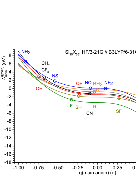
Fig. 3 shows the result of Eqs. III.2 and III.2, together with the data points of all ligands used in DFT calculations of Si35 NCs (Section III.3). Embedding in SiO2 vs. Si3N4 is indeed a good choice for a maximum NESSIAS. Coating LNS i-Si with Fluoride is even more attractive for a maximum electronic structure shift to higher as evident from the bigger difference in to Si3N4-embedding. Such differences as per embedding dielectric of LNS i-Si are useful to predict the adequate combination of dielectrics to arrive at type II homojunctions required for VLSI field effect transistors (FETs), e.g. using SiO2- and Si3N4-embedding, or potentially at band-to-band tunneling (BTBT) FET devices by replacing SiO2- with Fluoride-embedding.
Since Si and other semiconductors have a significant inter-atomic charge transfer, the NESSIAS effect will not be limited to a few atomic MLs, providing the basis for its use in VLSI electronics. Within the dielectric, a charge transfer over more than four Si–X (X O, N) MLs becomes unnotable in particular for SiO2 embedding König et al. (2018, 2019) because of the strong polar nature of the bonds and immobility of local charges due to charge localization and a rather wide bandgap of SiO2 and Si3N4.
III.3 Verification of the Analytic Relation with DFT Simulations
(a) (b)
(c) (d)
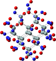
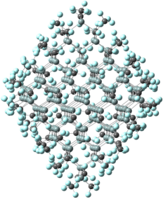
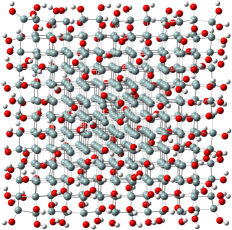
DFT approximants consist of NCs fully terminated with one ligand type. The main anion forms the center of the ligand and the interface bond to the NC. Relevant properties of main anions are listed in Table 2. Fig. 4 shows examples of NCs calculated by DFT.
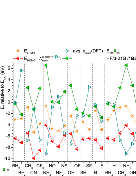
The dependence can be clearly seen for Si35 NCs with a diameter of nm as a function of their surface termination in Fig. 5, where ligands are grouped in accord with their main anion, and specific outer terminations where applicable, arranged for increasing EN from left to right. Recently, H-terminated 1.1 nm size Si NCs were processed by a top-down design Shirahata et al. (2020). For Si NCs fully terminated with BF2, CF3, NF2, and OF ligands, does not appear to follow as accurately. This behavior is explained in Ref. Sup . All other terminations are described accurately by .
We extended calculations of Si35 NCs to other hybrid DFs, the Heyd-Scuseria-Ernzerhof DF with its 2006 parametrization (HSE06) Krukau et al. (2006), and the B3LYP DF complemented with the Coulomb Attenuation Method (CAM-B3LYP) Yanai et al. (2004). Detailed results of such calculations are listed in Ref. Sup , further corroborating the accuracy of in predicting .
III.4 Details of the NESSIAS Effect in Si NWells from Experiment
III.4.1 Calibrating the NESSIAS by Measuring the Intrinsic Valence Band Edge with Synchrotron UPS
First data of SiO2- and Si3N4-embedded Si NWells were obtained by measuring the VB maximum (leading edge) of bulk Si and embedded Si NWells using scan ensembles of synchrotron UPS König et al. (2018, 2019, 2021) with their statistic data, whereby the VB maximum is located at point; . We now discuss the fine structure of UPS spectra, revealing a sub-edge which can be assigned to the Van Hove singularity of bulk Si at the L point in the BZ with its energy Chelikowsky et al. (1989); Ley et al. (1972). For NWells with nm, the VB subband structure becomes increasingly perturbed by QC. An assignment of subband Van Hove singularities near becomes a function of and of specific high symmetry points in the electronic DOS along non-orthogonal -directions of the NWell plane, in particular X and M, see Ref. Sup . Fig. 6 illustrates the change in VB electronic structure with the shrinking size of LNS i-Si using experimentally derived values. We focus on the energy offset between and L point for bulk Si, and between and X, M points for thin NWells, generally expressed by the term .
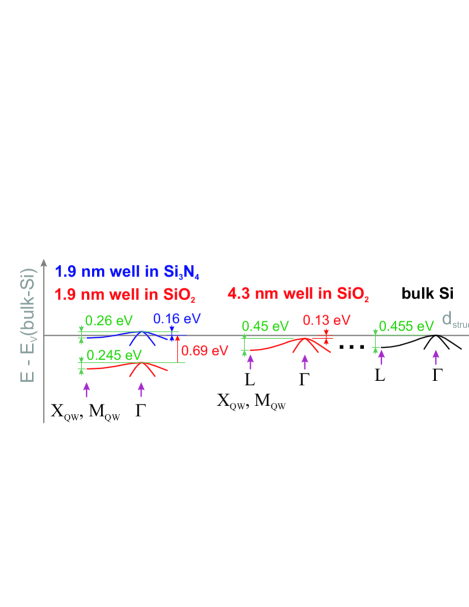
Fig. 7 shows that does not depend on the embedding dielectric as should be the case for a pure QC phenomenon with sufficiently high potential walls (i.e. band offsets between respective bulk phases) Schiff (1968), cf. Fig. 10(a).
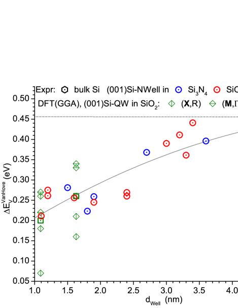
When QC sets in with decreasing , the energy offset between VB-DOS extrema at and adjacent Van Hove singularities diminishes as is shifted to higher binding energies. Since the adjacent Van Hove singularities already have higher binding energies with respect to the VB maximum, they do not experience a notable energy shift due to QC even for the minimum energetic distance of eV for NWells with nm, see Fig. 7. We can therefore take as a good estimate for the shift of to higher binding energies due to QC only. Interestingly, DFT-GGA calculations of Si NWell superlattices (SLs) with 1.9 nm thick SiO2 barriers Carrier et al. (2002) yield very similar values of , cf. Fig. 7 and discussion in Ref. Sup . Yet, the energy offset derived from UPS does not reflect the unperturbed QC case due to its finite energy difference, accounting for some uncertainty of the Van Hove singularity with higher binding energy Schiff (1968) as the reference level for . Still, this deviation on the order of 1 meV is further diminished by the DOS in the Brillouin zone (BZ) at L point in bulk Si being ca. five-fold bigger as compared to the DOS at point, see to UPS data for surface-cleaned bulk Si (Fig. S7, Ref. Sup ). Local deviations due to stress/strain and the deviation of of ca. nm around its nominal value have a more significant impact on , see Fig. 7. Hence, as measured by UPS is an accurate estimate of VB QC. We introduce a VB maximum as a function of NWell thickness,
In Fig. 7, a quadratic-hyperbolic least residuals fit was used in accord with QC theory Schiff (1968) to estimate the shift of as a function of .
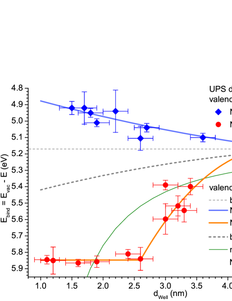
We present all UPS data together with in Fig. 8. The energy offset due to the NESSIAS as per embedding dielectric is clearly visible, saturating for SiO2-embedding for nm, while steadily growing with decreasing for Si3N4-embedding. The VB offset between 1.6 nm thick Si NWells coated with Si3N4 vs. SiO2 is eV, facilitating charge carrier separation on a massive scale in analogy to a steep p/n junction induced by impurity doping. Before discussing the full electronic structure of embedded Si NWells with experimental data, we revisit the discussion of the quantitative NESSIAS impact due to Si3N4 vs. SiO2.
With , we have a true reference level to investigate on a quantitative base how the NESSIAS affects Si NWells per embedding dielectric. To that effect, we calculate the absolute value of the difference between and the VB maximum per embedding dielectric, viz. cf. Fig. 9.
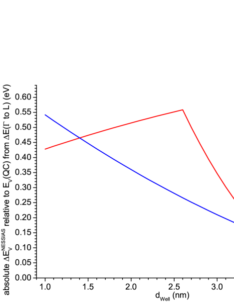
As already emerging from Fig. 8, becomes saturated for nm for NWells in SiO2. The strong localization of extrinsic electrons from the NWell at the O atoms in SiO2 has two effects. Due to the small localization volume which is limited to the immediate proximity of O atoms, see Section III.1, these atoms undergo electrostatic screening. Thereby, the ICT from the NWell to SiO2 is self-limiting. The NWell undergoes a rather strong positive ionization, increasing the attractive Coulomb force which works against the ICT. Together with the screened O atoms, the cumulative ICT charge thus decreases for nm, whereby its partition per Si NWell atom still increases. The latter statement is straightforward to see when comparing of nm with its value at half the NWell thickness. There, decreased from its maximum of 0.56 eV at nm not by about 0.28 eV as would be the case for a constant NWell ionization, but by a mere 0.10 eV, accounting for a further increase of the positive ionization per Si NWell atom. We note, though, that the electronic DOS of the VB over energy is not constant. Further decrease in may occur due to an increased DOS at the energy where resides. The situation is very different for Si3N4-embedding, where is constantly increasing for a decreasing , getting close to the saturation limit of SiO2-embedding. This behavior is in accord with the quantum-chemical properties of N, see Section III.1. It is uncertain whether we can proceed to Si3N4-embedded NWells with nm to find a saturation limit in experiment should it exist. What we do know from experiment is that the constant increase of with decreasing results from the electron-attractive, yet delocalizing nature of N which does not suffer from a saturation due to a much bigger volume which can be utilized by N to accommodate extrinsic electrons. As discussed in Section III.1, this peculiar behavior also results in a part of the ICT to be reflected back into the NWell as a consequence of the decreased binding energy of extrinsic electrons at N atoms, thereby shifting the electronic structure of the NWell and LNS i-Si in general towards .
We have stated in Section III.1 that 1 ML SiO2 can keep the NESSIAS saturated for a ratio of LNS i-Si atoms per interface bond of for Si NCs. Fig. 8 shows that this saturation is left around nm which corresponds to ca. 19 atomic ML of (001)Si or 38 Si atoms and eight interface bonds per unit cell area, resulting in . Assuming an exponential decay in charge transfer through SiO2 when moving away from the interface, we arrive at the estimate of ca. 3 ML or 0.9 nm SiO2 König et al. (2014, 2018) after which the NESSIAS does not increase significantly anymore by increasing the thickness of SiO2. While this is good news for the VLSI technology where ultrathin SiO2 layers are required to chemically passivate LNS i-Si and to establish the primary layer of gate dielectrics, there is little chance to extend a saturated NESSIAS in Si beyond nm. For Si3N4-embedding, the delocalizing impact of N yields to a NESSIAS smeared out over , with no saturation present for nm.
III.4.2 A First Glimpse on the Full NESSIAS Picture

(a)
(b)
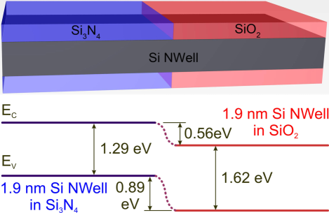
We recently started to measure the energy of the conduction band edge of Si NWells embedded in SiO2 by means of X-ray Absorption Spectroscopy in Total Fluorescence Yield mode (XAS-TFY) König et al. (2021). An initial sample of a Si3N4-coated NWell gave us a very first glimpse on the electronic structure of Si NWells of comparable thickness as a function of their embedding. We thus focus here on two NWell samples with nm and the respective embedding. Details of other SiO2-coated NWells can be found in König et al. (2021) and its supporting information, representative scans and statistical data of both samples used here can be found in Ref. Sup . The obtained experimental data for and are shown together with the bulk phases of Si, SiO2, and Si3N4 in Fig. 10(a). Fig. 10(b) shows a combination of both NWell samples, with the resulting band diagram as per experimental data from Fig. 10(a). Obviously, we can induce a strong type II homojunction Harrison (2009) in LNS i-Si merely by coating with SiO2 vs. Si3N4.
The band structures of bulk solids shown in Fig. 10(a) yield to further insights into the NESSIAS effect. The band offsets between the bulk phases of Si and SiO2 as well as Si and Si3N4 are somewhat asymmetric. A strong shift of , to higher binding energies occurs for SiO2. For Si3N4, we see a smaller shift to lower binding energies. Both observations are in accord with our discussion of O and N vs. Si in Section III.1. We thus can track the NESSIAS effect all the way to the bulk phase of the respective dielectric. As a consequence, the entire electronic structure of LNS i-Si such as a sufficiently thin NWell moves towards a more symmetric band offset with the respective dielectric when the NESSIAS effect becomes significant.
From above discussion, the question of a LNS i-Si size limit arises below which it starts to behave like the embedding dielectric to a degree where they depart from the properties of semiconducting Si. Further research efforts will be required to provide a thickness estimate around which the NESSIAS effect can be put to best use for technological applications from the viewpoint of LNS i-Si system size. Moreover, recent DFT calculations König et al. (2021) showed that other group IV semiconductors such as C and Ge – and presumably their alloys SiC and SiGe – strongly respond to the NESSIAS, offering a much broader impact on VLSI device design beyond LNS Si.
IV Conclusions
We quantitatively demonstrated that an energy shift of electronic states defining the CB and VB edge of low nanoscale intrinsic Si (LNS i-Si) exists, being considerably different from commonly assumed energy positions. The underlying Nanoscale Electronic Structure Shift Induced by Anions at Surfaces (NESSIAS) is brought about by the embedding dielectric, whereby N in the form of Si3N4 and O in the form of SiO2 are of particular scientific and technological interest. We explained the underlying quantum chemical processes of the NESSIAS which mainly reside with the anion of the dielectric, namely its ability to attract extrinsic electrons such as from LNS i-Si from afar (electronegativity EN defining the ionicity of bond to Si), and its ability to localize extrinsic electrons in its immediate vicinity (electron affinity ). Both, O and N attract extrinsic electrons from i-Si via an interface charge transfer. While such electrons get strongly localized at O with its highly negative , they get delocalized around N due to its being positive. Therefore, electronic states experience a shift to higher binding energies with O as an interface anion, while the delocalization of extrinsic electrons in the immediate vicinity of N reflects such states partly back to the LNS i-Si, lowering their binding energy. Due to these quantum chemical properties, the NESSIAS saturates rather quickly as a function of SiO2 thickness, while still increasing for Si3N4-coatings beyond three atomic MLs. The NESSIAS thus results in an electronic structure shift towards (away from) for Si3N4- (SiO2-) embedding. Hence, LNS i-Si systems like NWires König et al. (2021) or NWells can be flooded by holes (Si3N4-coated) or electrons (SiO2-coated), a property which readily offers the formation of a type II (p/n) homojunction in LNS i-Si.
We introduced an analytic parameter as a function of the ionization of the main interface anion which correctly predicts the HOMO energy of the LNS i-Si system as a function of the main interface anion, and verified its accuracy with three different hybrid DFs. As main anions to Si, we evaluated the entire 1st period of the periodic table and S, with all of these main anions terminated by all possible outer atoms to form ligands. Using to predict the NESSIAS as a function of the dielectric coating, we obtain optimum combinations of Si and dielectrics per design to meet the desired functionality of VLSI electronic devices. Such predictions are useful in particular for ultra-low power VLSI devices and ultimate cryogenic electronics as with NESSIAS, no dopants are required for a p/n junction to exist.
Band edges of 1.9 nm thick Si NWells measured by UPS and XAS-TFY revealed band offsets due to Si3N4- vs. SiO2-coating of eV and eV. The band gap energies were eV for Si3N4- and eV for SiO2-embedding, respectively. Looking at the evolution of experimental and values with decreasing , we showed that the band offsets of the NWells to the respective dielectric get more symmetric. It emerged that the absolute position of and residing with the respective dielectric is also a function of the quantum chemical properties at the origin of the NESSIAS. Detecting the NESSIAS in DFT calculations and in experiment requires the evaluation of and on an absolute energy scale. e.g. their position to . The impact length for a saturation of the NESSIAS is ca. nm per plane interface, resulting in nm thick Si NWells and nm thick Si NWires König et al. (2021). This short impact length and the lack of published DFT calculations and measurements with an absolute energy calibration are the likely reasons why the NESSIAS has not been detected until recently König et al. (2008, 2014, 2018). With VLSI approaching ultrathin fins and NWires, device dimensions are currently advancing into the thickness ranges mentioned above. It should therefore be of high interest to the VLSI research community to carry out device-related research, in particular in the light of the prospective ultra-low power demand and low temperature functionality given by the NESSIAS effect.
Acknowledgements.
D. K. acknowledges the 2018 Theodore-von-Kàrmàn Fellowship of RWTH Aachen University, Germany. M. F., N. W. and J. K. acknowledge support by the Impulse and Networking Fund of the Helmholtz Association. D.H. acknowledges funding via a Heisenberg grant by the Deutsche Forschungsgemeinschaft (DFG, German Research Foundation), project #434030435. I.P., F.B., and E.M. acknowledge funding from EUROFEL project (RoadMap Esfri) and thank Federico Salvador (IOM-CNR) for technical support. The authors acknowledge Elettra Sincrotrone Trieste for providing access to its synchrotron radiation facilities (through proposals #20165089, #20180054, #20190057, #20200079, #20205084, #20215072, and #20215081), and thank L. Sancin for technical support at Elettra, and Simone Dal Zilio for advise and use of the Micro and Nano fabrication facility FNF at IOM-CNR. D. K. and S. C. S. acknowledge the National Computational Infrastructure (NCI) for the generous computing resources allocated on the Gadi supercomputer, Australian National University, Canberra, Australia.Appendix A Derivation of the quantum Chemical Parameter to describe for Various Interface Ligands/Dielectrics
We set out by relating , and of the interface main anion of the ligand group to the average charge transferred from the LNS Si to the main anion :
For , we arrive at the trivial result that the regular electron affinity applies. The term stands for the ionization energy of the main anion which is counted positive towards ; and are counted negative (positive) when going below (above) . For avoiding confusion with the signs of , we use its absolute value. For , we include due to being increasingly substituted by , since a localized electron would have to fill up the vacant valency before it starts to present a real negative charge in the sense of an electron affinity. The influence of the cation is implicitly included in above equations via which depends on of the nominal cation (semiconductor structure), and in a few cases from its electron affinities when charge is transferred from the embedding material to the LNS semiconductor system, as is the case for SF2 or BF2 ligands in Fig. 5. This atypical behavior is due to the peculiar quantum chemical nature of F in ligands, see Ref. Sup for further discussion.
Equations A and A establish the principal relation to describe the NESSIAS effect. We now work out the dependence of on . To this end, we need a Coulomb term which is a function of localized at the main anion, leading to a Coulomb functional (Coulomb field) of a quasi-point charge distributed in a local atomic potential of the main anion, viz. . This approach requires a local potential to accomodate which is given by the Lennard-Jones potential Elliott (1998)
| (6) |
with being the minimum energy of the potential well, and being the inter-particle distance which refers to the inter-electron distance of the electron pair forming the single bond per main anion to the Si NC, see Fig. 11. The potential minimum occurs at , with set to 0.05 nm as an example.
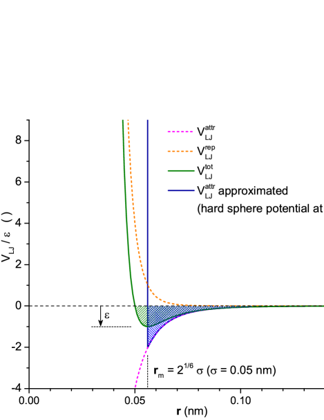
In our investigation of the anion impact, we will focus on the attractive part of , namely which can enable or prevent the localization of an external electron, depending on the charge state and outer termination of the main anion. Since we do not have the exact inter-particle distance of the two electrons forming the Si-anion bond (nor does this make much sense from a quantum mechanical viewpoint), and varies as per anion type and its charge state, we work with proportionalities in analogy to solving a partial fraction decomposition by comparison of coefficients Zeidler et al. (2004). The scaling of such proportionality relations are given by , , and at , 0, and , respectively. We approximate by a hard-sphere potential of at , and for . The exact and the approximated well potentials integrated over their outward spatial extension should be possibly identical to ensure an adequate description of charge localization. As shown in Appendix Section A.1, the spatial extension of the well of the approximated deviates from by a mere 2.9 %. No boundary conditions are needed as integration limits since we scale the proportionality relations with quantum chemical properties as per above, merely requiring the correct description of all variables in powers of . For the accumulated (or depleted) charge , we integrate over its location, viz.
Due to their comparatively big distance as compared to the localized anionic charge, we can approximate the Coulomb field of the main anion onto NC atoms as a point charge, yielding
| (8) |
where is the elementary charge presenting the probe charge into which the Coulomb field exerts its impact, and is the permittivity constant of vacuum. We thus get describing an energy gradient which will become more apparent below.
Next, we provide a gauge for the interface impact on an atomic scale, i.e. an area density of potential energy due to charge accumulation/depletion at the main anion which influences the electronic structure of the NC atoms. Such density is given by the quotient of the Coulomb impact onto the NC and the charge localization at the main anion:
| (9) | |||||
Equation 9 presents a Coulomb pressure onto the NC in analogy to a force constant conveying the exertion of force onto a mechanical system: An increased results in an increased which will impact upon the probe charge , whereby the location of resides with , thereby scaling the impact of the quantum chemical properties of the main anion, viz. , and . With relation 9 describing an area density of Coulomb energy, we substitute in Eqs. A and A with , ending up with
which are equivalent to Eqs. III.2 and III.2 in the main article.
A.1 Comparison of Well Potentials – vs. Approximated
For comparing both well areas, we integrate the respective potential over with its integration limits, yielding
for the well formed by the Lennard-Jones potential, and
for the well described by the hard sphere potential approximating . With being the exact potential, we arrive at
| (14) |
yielding 1.0289, i.e. a deviation of the approximated well area from the exact Lennard-Jones well of ca. 2.9 %.
References
- König et al. (2018) D. König, D. Hiller, N. Wilck, B. Berghoff, M. Müller, S. Thakur, G. D. Santo, L. Petaccia, J. Mayer, S. Smith, and J. Knoch, Beilstein J. Nanotech. 9, 2255 (2018).
- König et al. (2019) D. König, N. Wilck, D. Hiller, B. Berghoff, A. Meledin, G. D. Santo, L. Petaccia, J. Mayer, S. Smith, and J. Knoch, Phys. Rev. Appl. 12, 045050 (2019).
- König et al. (2021) D. König, M. Frentzen, N. Wilck, B. Berghoff, I. Píš, S. Nappini, F. Bondino, M. Müller, S. Gonzalez, G. D. Santo, L. Petaccia, J. Mayer, S. Smith, and J. Knoch, ACS Appl. Mater. Interfaces 13, 20479 (2021).
- Note (1) It is interesting to note in this context that the VLSI technology nodes do not reflect the physical gate length. We have a planar MOSFET model shrunken to a size where it would perform as the fin-FET of the respective technology node Col (2016).
- Ladd et al. (2010) T. D. Ladd, F. Jelezko, R. Laflamme, Y. Nakamura, C. Monroe, and J. L. O’Brien, Nature 464, 45 (2010).
- Garcia-Castello et al. (2015) N. Garcia-Castello, S. Illera, J. D. Prades, S. Ossicini, A. Cirera, and R. Guerra, Nanoscale 7, 12564 (2015).
- Jarolimek et al. (2017) K. Jarolimek, E. Hazrati, R. A. de Groot, and G. A. de Wijs, Phys. Rev. Appl. 8, 014026 (2017).
- Ossicini et al. (2020) S. Ossicini, I. Marri, M. Amato, M. Palummo, E. Canadell, and R. Rurali, Faraday Discuss. 222, 217 (2020).
- Halilov et al. (2020) S. Halilov, M. L. Belayneh, M. A. Hossain, A. A. Abdallah, B. Hoex, and S. N. Rashkeev, RSC Adv. 10, 22377 (2020).
- König et al. (2022) D. König, D. Hiller, and S. Smith, Phys. Stat. Sol. B 259, 2100549 (2022).
- Lee et al. (2012) B. G. Lee, D. Hiller, J.-W. Luo, O. E. Semonin, M. C. Beard, M. Zacharias, and P. Stradins, Adv. Funct. Mater. 22, 3223 (2012).
- Thoan et al. (2011) N. H. Thoan, K. Keunen, V. V. Afanas‘ev, and A. Stesmans, J. Appl. Phys. 109, 013710 (2011).
- Basaa et al. (2000) D. K. Basaa, M. Bose, and D. N. Bose, J. Appl. Phys. 87, 4324 (2000).
- Jung et al. (2011) S. Jung, D. Gong, and J. Yi, SOLMAT 95, 546 (2011).
- Deal and Grove (1965) B. E. Deal and A. S. Grove, J. Appl. Phys. 36, 3770 (1965).
- Kern and Deckert (1978) F. W. Kern and C. A. Deckert, in Thin film processes, edited by V. L. Vossen and W. Kern (Academic Press, New York, 1978) Chap. 5, pp. 411–413.
- Kräuter et al. (1998) G. Kräuter, A. Schumacher, and U. Gösele, Sensors and Actuators A 70, 271 (1998).
- Zangrando et al. (2004) M. Zangrando, M. Zacchigna, M. Finazzi, D. Cocco, R. Rochow, and F. Parmigiani, Rev. Sci. Instr. 75, 31 (2004).
- Stebel et al. (2011) L. Stebel, M. Malvestuto, V. Capogrosso, P. Sigalotti, B. Ressel, F. Bondino, E. Magnano, G. Cautero, and F.Parmigiani, Rev. Sci. Instr. 82, 123109 (2011).
- (20) See Supplemental Material for additional data on DFT calculations for Si NCs of various sizes and surface terminations using different DFs, details on UPS measurements including DFT data supporting , details on XAS-TFY measurements.
- Petaccia et al. (2009) L. Petaccia, P. Vilmercati, S. Goronikov, M. Barnaba, A. Bianco, D. Cocco, C. Masciovecchio, and A. Goldoni, Nucl. Instr. Meth. in Phys. Res. A 606, 780 (2009).
- Acc (2020) “Nanofilm_ep4, MICROSCOPIC THIN FILM METROLOGY AND VISUALIZATION,” (2020), https://www.accurion.com/accurion_broschuere_EP4_201906.pdf ; accessed , see page 6 ’self-assembled monolayers’.
- Mueller (1948) H. Mueller, J. Opt. Soc. Am. 38, 661 (1948).
- Azzam (1978) R. M. A. Azzam, J. Opt. Soc. Am 68, 1756 (1978).
- Savenkov (2009) S. N. Savenkov, in Light Scattering Reviews, Vol. 4, edited by A. A. Kokhanovsky (Springer, Berlin, 2009) Chap. 3, pp. 71–119.
- Thust et al. (2016) A. Thust, J. Barthel, and K. Tillmann, Journal of large-scale research facilities JLSRF 2, A41 (2016), DOI: 10.17815/jlsrf-2-66.
- G09 (2012) Gaussian09, Revision D.01, M. J. Frisch, et. al., Gaussian, Inc., Wallingford, CT (2012).
- Dennington et al. (2009) R. Dennington, T. Keith, and J. Millam, “GaussView 5.0.8,” (2009).
- Hartree (1928a) D. R. Hartree, Proc. Cambr. Phil. Soc 24, 89 (1928a).
- Hartree (1928b) D. R. Hartree, Proc. Cambr. Phil. Soc 24, 111 (1928b).
- Fock (1930) V. Fock, Zeitschr. Phys. 61, 126 (1930), in German.
- Gordon et al. (1982) M. S. Gordon, J. S. Binkley, J. A. Pople, W. J. Pietro, and W. J. Hehre, J. Am. Chem. Soc. 104, 2797 (1982).
- Becke (1988) A. D. Becke, Phys. Rev. A 38, 3098 (1988).
- Lee et al. (1988) C. Lee, W. Yang, and R. G. Parr, Phys. Rev. B 37, 785 (1988).
- Becke (1993) A. D. Becke, J. Chem. Phys. 98, 5648 (1993).
- Yanai et al. (2004) T. Yanai, D. P. Tew, and N. C. Handy, Chem. Phys. Lett. 393, 51 (2004).
- Krukau et al. (2006) A. V. Krukau, O. A. Vydrov, A. F. Izmaylov, and G. E. Scuseria, J. Chem. Phys. 125, 224106 (2006).
- Francl et al. (1982) M. M. Francl, W. J. Pietro, W. J. Hehre, J. S. Binkley, D. J. DeFrees, J. A. Pople, and M. S. Gordon, J. Chem. Phys. 77, 3654 (1982).
- König et al. (2014) D. König, D. Hiller, S. Gutsch, and M. Zacharias, Adv. Mater. Interfaces 1, 1400359 (2014).
- Mönch (2001) W. Mönch, Semiconductor Surfaces and Interfaces, 3rd ed. (Springer, Berlin, 2001).
- Campbell et al. (1996) I. H. Campbell, S. Rubin, T. A. Zawodzinski, J. D. Kress, R. L. Martin, D. L. Smith, N. N. Barashkov, and J. P. Ferraris, Phys. Rev. B. 54, R14321 (1996).
- König et al. (2008) D. König, J. Rudd, M. A. Green, and G. Conibeer, Phys. Rev. B 78, 035339 (2008).
- König et al. (2009) D. König, J. Rudd, M. A. Green, and G. Conibeer, Solar Energy Mater. & Solar Cells 93, 753 (2009).
- Holleman et al. (1995) A. F. Holleman, E. Wiberg, and N. Wiberg, Lehrbuch der Anorganischen Chemie, 101st ed. (Walter deGruyter, Berlin, 1995) in German.
- Scheer et al. (1998) M. Scheer, R. C. Bilodea, and H. K. Haugen, Phys. Rev. Lett. 80, 2562 (1998).
- Guo and Whitehead (1990) Y. Guo and M. A. Whitehead, Can. J. Chem. 68, 1585 (1990).
- Huheey (1983) J. E. Huheey, ed., Inorganic Chemistry, 3rd ed. (Harper & Row, New York, 1983) appendix 5.
- Ginsberg and Miller (1958) A. P. Ginsberg and J. M. Miller, J. Inorg. Nucl. Chem. 7, 351 (1958).
- Brar et al. (1996) B. Brar, G. D. Wilk, and A. C. Seabaugh, Appl. Phys. Lett. 69, 2728 (1996).
- Shirahata et al. (2020) N. Shirahata, J. Nakamura, J. i. Inoue, B. Ghosh, K. Nemoto, Y. Nemoto, M. Takeguchi, Y. Masuda, M. Tanaka, and G. A. Ozin, Nano Lett. 20, 1491 (2020).
- Chelikowsky et al. (1989) J. R. Chelikowsky, T. J. Wagener, J. H. Weaver, and A. Jin, Phys. Rev. B 40, 9644 (1989).
- Ley et al. (1972) L. Ley, S. Kowalczyk, R. Pollack, and D. A. Shirley, Phys. Rev. Lett. 29, 1088 (1972).
- Schiff (1968) L. I. Schiff, Quantum Mechanics, 3rd ed. (McGraw-Hill, Singapore, 1968) pp. 39.
- Carrier et al. (2002) P. Carrier, L. J. Lewis, and M. W. C. Dharma-wardana, Phys. Rev. B 65, 165339 (2002).
- Kurata et al. (1981) H. Kurata, H. Masataka, and Y. Osaka, Jap. J. Appl. Phys. 20, L811 (1981).
- Iqbal et al. (1987) A. Iqbal, W. B. Kackson, C. C. Tsai, J. W. Allen, and C. W. B. Jr., J. Appl. Phys. 61, 2947 (1987).
- Keister et al. (1999) J. W. Keister, J. E. Rowe, J. J. Kolodziej, H. Niimi, T. E. Madey, and G. Lucovsky, J. Vac. Sci. Tech. B 17, 1831 (1999).
- Nicollian and Brews (1982) E. H. Nicollian and J. R. Brews, MOS (Metal Oxide Semiconductor) Physics and Technology (Wiley, New York, 1982).
- Ibach and Rowe (1974) H. Ibach and J. E. Rowe, Phys. Rev. B 10, 710 (1974).
- Harrison (2009) P. Harrison, Quantum Wells, Wires and Dots, 2nd ed. (Wiley, Chichester, 2009) pp. 11.
- Elliott (1998) S. Elliott, The Physics and Chemistry of Solids (Wiley & Sons, Chichester, 1998).
- Zeidler et al. (2004) E. Zeidler, W. Hackbusch, and H. R. Schwarz, Oxford User’s Guide to Mathematics (Oxford University Press Inc., New York, 2004) translated from German by Bruce Hunt.
- Col (2016) (2016), J.-P. Collinge, Tyndall National Institute, Cork, Ireland; private communication.