Observation of type-III corner states induced by long-range interactions
Abstract
Long-range interactions (LRIs) are ubiquitous in nature. Higher-order topological (HOT) insulator represents a new phase of matter. A critical issue is how LRI dictates the HOT phases. In this work, we discover four topologically distinct phases, i.e., HOT phase, the bound state in the continuum, Dirac semimetal (DSM) phase, and trivial insulator phase in a breathing kagome circuit with tunable LRIs. We find an emerging type-III corner state in the HOT phase, which splits from the edge state continuum and originates from the strong couplings between nodes at different edges. We experimentally detect this novel state by impedance and voltage measurements. In the DSM phase, the Dirac cone exhibits an itinerant feature with a tunable position that depends on the LRI strength. Our findings provide a deeper understanding of the LRI effect on exotic topological states and pave the way for regulating interactions in topolectrical circuits.
I introduction
Long-range interactions (LRIs) typically represent the two-body potential decaying algebraically at large distances with a power smaller than the spatial dimension. Paradigms of LRIs include electromagnetism, gravity, 2D vortices, etc. Physical systems with LRIs can exhibit many peculiar properties in their dynamics and statistics, such as negative specific heat and temperature jumps Campa2009 ; French2010 . Recently, the LRIs have been shown to impose certain effects on the topological states Varney2010 ; Beugeling2012 ; Li2019 ; Shen2021 ; Olekhno2022 ; Yu2017 ; Leykam2018 . For instance, Li et al. observed a type-II corner state in the photonic breathing kagome crystal in the presence of a weak LRI Li2019 . An open question is how a strong enough LRI dictates the topological phase. Quantum-optical technology may be a choice to address this issue with controllable spin-spin interactions, but it is difficult to implement in experiments Sandvik2010 ; Britton2012 .
Recently, electrical circuit manifests as an exceptional platform to study topological physics Olekhno2022 ; Jia2015 ; Albert2015 ; Imhof2018 ; Ezawa2018 ; Lee2018 ; Hadad2018 ; Hofmann2019 ; JBao2019 ; WZhang2020 ; Helbig2020 ; Liu2020 ; Olekhno2020 ; Song2020 ; Yang2020 ; SLiu2020 ; RChen2020 ; Zhang2020 ; Yang2021 ; Yangyt2021 ; Yang2022 ; Ventra2022 ; Wu2022 ; NAO2022 ; Galeano2022 ; Pei2022 ; Zhang2022 , which can imitate the tight-binding (TB) model in condensed matter physics by the inductor-capacitor () network. Conveniently, one can introduce an arbitrary hopping term between different nodes in the circuit. For example, the higher-order topological (HOT) insulators have been widely explored in circuits Imhof2018 ; Ezawa2018 ; JBao2019 ; WZhang2020 ; Song2020 ; Yang2020 ; SLiu2020 ; RChen2020 , which however focused on short-range interactions or hoppings.
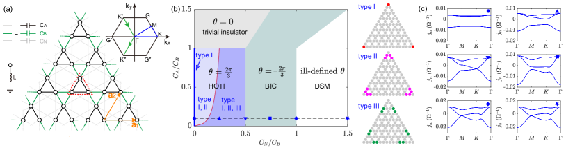
It is thus interesting to establish a fruitful connection between these two different topical areas of physics, i.e., LRIs and HOT phases. In this work, we investigate how LRIs affect the HOT insulators both in theory and experiment. To this end, we first derive the full phase diagram which includes four topologically distinct phases in the breathing kagome circuit with LRIs, specifically, a HOT phase, a bound state in the continuum (BIC, higher-order topology supporting corner-localized bound states in the continuum WABenalcazar2020 ), a Dirac semimetal (DSM) phase, and a trivial insulator phase. Interestingly, the HOT phase can be further classified into three types of corner states. The type-I corner states are pinned to zero admittance due to the protection of the generalized chiral symmetry, and they are localized at the three vertexes of the lattice. The type-II and type-III corner states are at finite admittances and split from the edge state continuum, which are akin to the edge states but exponentially decaying away from the 2nd and 3rd cells along the boundary, respectively [see the 2nd and 3rd subfigures in Fig. 3(d)]. Moreover, the type-II corner states separate from the lowest and highest edge modes and appear for an arbitrary LRI. By contrast, the type-III ones split from the edge state continuum only in the strong-coupling region, namely, a critical LRI value is required to move them out of the edge band. By measuring the impedance distribution and the voltage signal propagation, we directly observe all three types of corner states in experiments. In addition, we numerically identify the BIC and DSM phases. We show that the position of the Dirac points depends on the strength of LRI, which may help to control the transport behaviors of Dirac states.
The paper is organized as follows. In Sec. II, we present the circuit model and derive the full phase diagram. The emerging corner states are analyzed in Sec. III. We perform experimental measurements in Sec. IV. Conclusions are drawn in Sec. V. Technical details are given in Appendixes.
II Circuit model and phase diagram
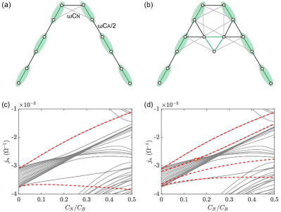
As shown in Fig. 1(a), we consider an infinite breathing kagome circuit with LRIs, by introducing next-nearest-neighbor (NNN) hopping terms (capacitors ) to the lattice. The NNN interactions can be regarded as LRIs for two reasons. In most topological systems with true LRIs, one can consider the NNN hopping terms without missing the key physics, because higher-order terms beyond NNN can only contribute negligible effects Li2019 ; Shen2021 . Besides, the concept of LRI very recently has been adopted in systems with NNN interactions Olekhno2022 . Labelling the nodes of the circuit by the response at frequency follows Kirchhoff’s law: , with the external current flowing into node , the voltage at node , and being the circuit Laplacian: with the capacitance between nodes and , and being the grounded inductance at node . The sum is taken over all connected nodes. The dashed red triangle represents the unit cell including three nodes, with the first Brillouin zone (BZ) plotted in the inset of Fig. 1(a). For convenience, we express as , with akin to the Hermitian TB Hamiltonian expressed as
| (1) |
where and represent the NN and NNN coupling Hamiltonian, respectively (see Appendix A for details). Next, as suggested in Refs. Hatsugai2011 ; Kariyado2018 ; Kudo2019 ; Araki2020 , we use Berry phase to distinguish these phases in the parameter space (here is the - plane), which is computed by
| (2) |
where is the Berry connection: with being the eigenvector of (1) for the lowest band. is an integral path in BZ: , shown by the green line segment in the inset of Fig. 1(a) (see Appendix A for discussion). The computation of Berry phase is displayed in Fig. 1(b). Here, we obtain three different Berry phases, i.e., , , , and an ill-defined value, filled by blue, green, gray, and white colors, respectively. Specifically, denotes the HOT phase, indicates the BIC phase (see Appendix B), and is the trivial insulator phase. The ill-defined belongs to the DSM phase owing to the gapless band structures ( Berry phase can only be rigorously defined for a gapped system. In the presence of strong NNN couplings, the lowest two bands touch each other. One thus cannot have a well-defined ). It is noted that, in the absence of the NNN coupling, one can only observe the type-I corner state and trivial phase by tuning the ratio Yang2020 . However, by adjusting certain capacitances of or in this lattice by breaking the crystal symmetry (such as symmetry), one may expect some peculiar edge states as illustrated in Ref. Yang2022 .
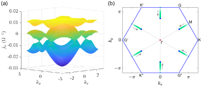
Figures 1(c) displays the band structures for different capacitance ratio at [blue symbols in Fig. 1(b)]. For , in the absence of NNN hopping term (), the band structures are gapped, which belongs to the HOT phase Yang2020 . As we increase the capacitance , the lowest two bands firstly converge at point at and reopen beyond it, and then close again at point when (see Appendix A). The degenerate point subsequently moves along the trace, forming the DSM state (see Appendix C). This phenomenon may provide a feasible method to manage the unique transport properties of itinerant Dirac states, in exploring the physics of anomalous quantum Hall effect Zhang2005 , minimum conductivity Ando2002 ; Tworzydlo2006 , and Klein tunneling Katsnelson2006 ; Stander2009 . For , the two gapless thresholds appear at and , and the behaviors of band structures are similar to the foregoing ones (not shown). Below, we focus on the HOT phase, i.e., and [blue region in Fig. 1(b)].
III Corner states
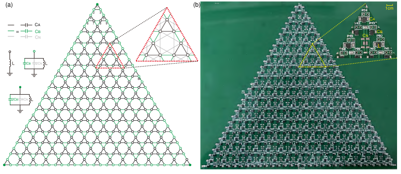
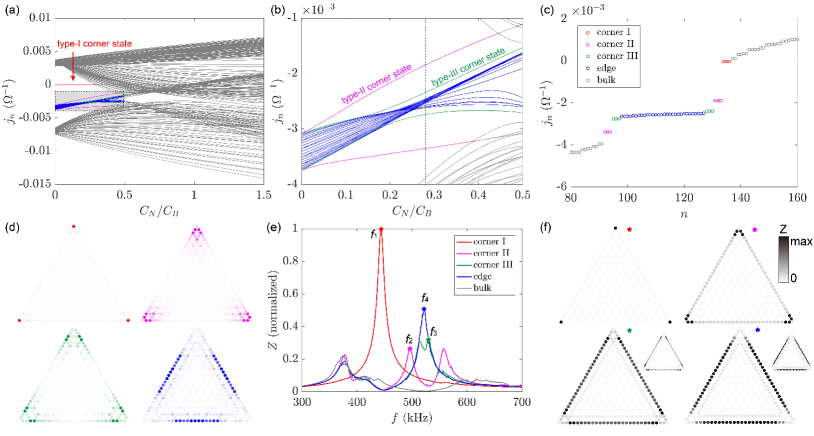
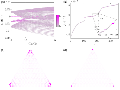
To observe the corner states, we consider a finite-size circuit network with nodes with the configuration being shown in Fig. 2(a). Diagonalizing the circuit Laplacian , we obtain both the admittance spectrum and wave functions. In the following calculations, we consider with nF. Figure 3(a) shows the admittance spectrum for different NNN hopping strengths. Except for the isolated zero-admittance mode (red segment), the other two modes (magenta and green segments) escape from the edge spectrums, which represent the type-II and type-III corner states, see Fig. 3(b) for details. We demonstrate that the type-II corner states appear for any , while the type-III corner states emerge only when with the critical value, as shown by the dark blue region in Fig. 1(a) (see Appendix D for details). In Ref. Li2019 , the same lattice is constructed in a photonic system but with a rather weak LRI. Therefore, only the type-II corner states were observed there, and they split from both the lowest and highest boundary modes. In order to find the type-III corner states, one needs a stronger LRI, and the circuit then exhibits its superiority for such a purpose. The strong NNN interactions induce strong couplings between nodes at different edges, so the internal edge modes can separate from the edge state continuum and form the type-III corner states.
Next, we analyze a representative example at [the dashed black line in 3(b)]. Specifically, we choose nF and H. The admittances are depicted in Fig. 3(c), with five kinds of eigenmodes donated by red, magenta, green, blue, and gray circles, corresponding to type-I corner, type-II corner, type-III corner, edge, and bulk states, respectively. It is noted that the type-I corner states are pinned to zero admittance, while type-II and type-III corner states are at finite admittances. Figure 3(d) shows the wave functions of the corner states and edge states, from which one can distinguish them clearly. The wave functions of the type-II (type-III) corner states are resembling those of the edge states, which have been proved to be topological Ni2019 ; Li2019 , but exponentially decaying away from the 2nd (3rd) cell along the boundary. This behavior can be viewed as the boundary states of the topological edge modes, i.e., the corner states.
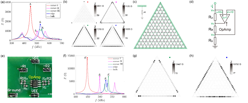
In an electrical circuit, one can use the impedance between the node and ground to reflect the mode near the zero admittance Lee2018 ; Yang2020 ; Yang2021 . In order to observe the different states mentioned above, one can shift the corresponding modes to zero admittance by changing the driving frequency without modifying the wave functions. Here, we adopt the impedance between the 1st, 3rd, 9th, 84th, 78th nodes and the ground to quantify the signals from the type-I corner, type-II corner, type-III corner, edge, and bulk states [see numbered nodes in Fig. 2(a)], respectively. Figure 3(e) shows the theoretical impedance as a function of the driving frequency, in which the red, magenta, green, blue, and gray curves denote the signal from the aforementioned five nodes, respectively. It is noted that we consider the quality factor ( factor) of inductor here with the value measured in the experiment. One can see that the impedance peaks of the type-I, type-II, type-III, and edge states appear at kHz, kHz, kHz, and kHz, respectively, marked by four colored pentagrams, which means the four states close to zero admittance at these frequencies.
We calculate the distributions of the impedance at and , with the results plotted in Fig. 3(f). At frequency kHz, the type-I corner modes are pinned at zero admittance. We depict the distribution of impedance at the resonant frequency in the first subfigure of Fig. 3(f). The impedances concentrate on the three vertexes of the sample, which confirms the existence of the type-I corner states. For type-II corner states, we find the distributions of the impedance are identical to the corresponding eigenmode profiles at frequency . However, the impedance curve of the edge state behaves as an extension and submerges the type-III corner states due to the finite factor of inductor. Therefore, the distributions of the impedance for type-III corner states seem to sprinkle throughout the edge. To distinguish the type-III corner states from edge states, one needs to improve the factor of inductors. We plot the distributions of impedance with higher -factor inductors () in the insets of Fig. 3(f), then one can distinguish the type-III corner states from the edge states. Next, we verify these numerical results by experiments.
IV Experiment
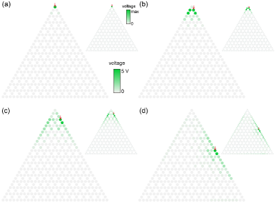
As shown in Fig. 2(b), we manufacture a printed circuit broad (PCB) to observe three kinds of corner states. To directly compare with the numerical calculations, we choose the same electric elements as those in theoretical analysis, but each circuit element has a natural 2% tolerance. The impedance of circuit is measured by the impedance analyzer (Keysight E4990A). Figure 4(a) shows the experimental impedances at different driving frequencies. Similarly, we adopt the impedances between the 1st, 3rd, 9th, 84th, 78th nodes and the ground to characterize the type-I corner (red curve), type-II corner (magenta curve), type-III corner (green curve), edge (blue curve), and bulk (gray curve) states, respectively. The experimental results are fully consistent with the numerical ones. Then, we measure the distribution of impedance at four frequencies marked by red, magenta, green, and blue pentagrams in Fig. 4(a), with the results plotted in Fig. 4(b). One can observe the type-I corner states, type-II corner states clearly, but the type-III corner states mix with the edge states due to the low factor.
The factor of an inductor is defined as , where the comes from inevitable losses. To compensate for the dissipation, we introduce active elements to the boundary nodes [light green region in Fig. 4(c)], realized by connecting a series of negative resistances with the configuration shown in Figs. 4(d) and 4(e) (see Appendix E). We numerically compare two cases that in introduced to all nodes and to boundary nodes only, which gives almost identical results. We therefore only add negative resistances to edge nodes to reduce the experimental complexity. As a consequence, the effective -factor of inductors is improved to about 150, so the impendence peak becomes very sharp, with the peak value being enhanced by about 400%, as shown in Fig. 4(f). We then measure the distribution of impedance at frequency and again and clearly separate the type-III corner states from the edge states, see Figs. 4(g) and 4(h). From these experimental results, we find that all corner states are robust against the disorder because the elements intrinsically have 2% tolerance.
To directly observe the dynamic response of the circuit, we measure the propagation of the voltage signals for all three corner states and edge states. As shown in Fig. 5(a), we impose a voltage signal at the first node (labeled by red arrow) by with the amplitude V and by an arbitrary function generator (GW AFG-3022), and measure the amplitudes of the steady voltage sign by the oscilloscope (Keysight MSOX3024A) over the whole sample. We find that the signal is only localized at the first node, indicating the type-I corner state. With the same method, we futher observe the type-II corner, type-III corner, and edge states at frequency at the , , and , with the results plotted in Figs. 5(b)-5(d), respectively. Meanwhile, we show theoretical results in the insets of each subfigure for comparison, which agree well with experimental findings.
V Conclusion
To summarize, we investigated the effect of LRIs on the topological phases in breathing kagome circuits. With appropriate LRIs, we discovered the type-III corner state and presented a direct experimental observation. We showed that the type-III corner states split from the edge modes, and originate from the strong coupling between nodes at different edges. With stronger LRIs, the BIC and DSM phases subsequently emerge in this system. Our results highlighted the important role played by LRI in topological phases and phase transitions. Our findings significantly advance the understanding of the localization behavior of HOT states and may spur future studies in other systems, such as acoustic lattices, photonic crystals, and cold atoms, and in higher dimensions allowing peculiar hinge states and Weyl semimetal states. It is worth mentioning that the NNN hopping terms in our system differ from the LRIs in the field of strongly correlated electrons that are closely related to local and non-local density interactions. LRIs beyond long-range hopping may exhibit other appealing properties, which deserve thorough exploration in the future.
Acknowledgements.
ACKNOWLEDGEMENTS
This work was supported by the National Natural Science Foundation of China (Grants No. 12074057, No. 11604041, and No. 11704060).
APPENDIX
Appendix A The generalized chiral symmetry, Berry phase and phase transitions
As shown in Fig. 6, the NN coupling Hamiltonian is given by
| (3) |
with the matrix elements
| (4) | ||||
where is the wave vector in the directions, and
| (5) |
with the matrix elements
| (6) | ||||
It can be verified that satisfies the generalized chiral symmetry at resonant frequency , because of , , , with . If we add the diagonal element to , the resonant frequency will shift from to . We find that the remainder of still holds the generalized chiral symmetry. It is to say that the periodic NNN hopping terms do not break the generalized chiral symmetry but only cause a shift of the resonant point, which provides topological protection for the triply degenerate zero-admittance mode.
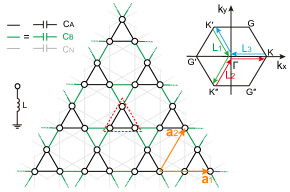
Next, we discuss the relationship between the symmetry and the quantized Berry phase. The Berry phase is closely related to the local twist of the Hamiltonian Hatsugai2011 , which is quantized due to time-reversal symmetry and inversion symmetry, for instance. In the breathing kagome lattice, it has symmetry, so the points , , in the Brillouin zone are equivalent, as shown in the inset of Fig. 6. So, there are three equivalent paths for computing Berry phase: : , : and : . As a result, the Berry phases should take the same value, i.e., . In addition, the integral along the path is equal to zero, i.e., . Therefore, we obtain the quantized Berry phase with .
To show the details of phase transition at and points, we analyze the eigenvalues and wave functions at these two points. At point, the admittance spectra are given by , , and with the corresponding wave functions expressed as , and . We find that the lowest band exchanges from to at [the first phase transition in Fig. 1(b)]. Meanwhile, the expectation value of the phase of wave functions for the lowest band ) Ni2019 changes from to (same as the Berry phase), where is the three-fold rotational operator.
At point, the admittance spectra are , , and with the eigenmodes , , and . Here . The lowest two bands close at , accompanied by the exchange of the lowest band from to and the wave functions from to [the second phase transition in Fig. 1(b)]. In the case of , the lowest two bands touch each other and form the semimetal states. For the trivial state, the wave-function phase is always equal to 0.
Appendix B Bound state in the continuum
In Fig. 3(a), one cannot find any isolated mode in the range of [green region in Fig. 1(b)]. However, if we evaluate the inverse participation ratio (IPR)
| (7) |
of the system, where is the normalized wave function with , we find localized states buried in the bulk and edge continuum, as shown in Fig. 7(a). The IPR has been widely adopted to study Anderson localization in disordered systems Janssen1998 , and to confirm the existence of HOT states recently HAraki2019 ; Wakao2020 . Taking as an example, we find two groups of localized states appearing in the continuum, as shown in Fig. 7(b). We plot their wave functions in Figs. 7(c) and 7(d), respectively. We confirm that both localized states actually are corner states.
Appendix C Dirac semimetal state
To illustrate the DSM state, we plot the band structure of an infinite kagome circuit in Fig. 8(a). The lowest two bands linearly touch each other at six points, which corresponds to the DSM state. Besides, by tuning the capacitance , we find that the positions of the six Dirac points continuously move (one of them moves along the path ), see Fig. 8(b).
To obtain an analytical understanding, we begin with Hamiltonian (1), and rewrite it as a concise form
| (8) |
with , , and [see Eq. (4) and Eq. (6) for details]. The secular equation is given by
| (9) |
For a cubic equation, if the discriminant is satisfied, it must have three real roots with two degenerate ones. Imposing , the matrix elements and can be simplified as
| (10) | ||||
Divided by , the above equations are expressed as
| (11) | ||||
with and . The discriminant is simplified as . Substituting the expressions of to this equation, we get
| (12) |
The solution is given by
| (13) |
At , we have (). In the case of (), the value of the right part of Eq. (13) is greater (less) than 1, so we can obtain a real solution of only for . In the limit of , we obtain and , which is the terminal of the Dirac points. We therefore prove that the solution is indeed the trajectory of the Dirac points. Due to the symmetry of the lattice, the other two equivalent traces of Dirac points exist along the lines of and , respectively. To show the linear touching of lowest two bands, we consider the circumstance of with Dirac points at and , marked by the blue dots in Fig. 8(b). In such a case, we can analytically solve the band structure as
| (14) | ||||
In the vicinity of the Dirac points, one can expand the lowest two bands [] as
| (15) |
with , and . One can clearly see a linear band crossings near the Dirac points.
Appendix D Origin of the type-II and type-III corner states
To explain the origin of the type-II corner states, we consider the first-order perturbation theory as shown in Fig. 9(a). The perturbation Hamiltonian is given by
| (16) |
Diagonalizing the above matrix, we obtain the perturbation solution
| (17) |
with the results plotted by dashed red lines in Fig. 9(c). The two solutions are type-II corner states. The NNN couplings cause an effective interaction () between two dimers across the corner, which splits the type-II corner states from the edge spectrums.
For type-III corner states, we have to consider the second-order perturbation theory as shown in Fig. 9(b). The system is described by a Hamiltonian matrix (not shown). By diagonalizing it, we obtain the dashed red spectrums in Fig. 9(d), which can explain the type-III corner states well. The NNN couplings induce extra interactions to edge nodes by connecting to the bulk nodes, which yields the type-III corner states.
To study the band splittings, we consider three Su-Schrieffer-Heeger (SSH) models Ventra2022 as shown in Fig. 10(a), described by the following Hamiltonian (, we set )
| (18) |
| (19) |
| (20) |
The hopping terms cause the splitting of the boundary modes as , which can be approximatively regarded as an effective capacitances , and to directly connect the two boundary nodes, as the red arrows shown in Fig. 10(a). Next, we will show how these connections induce the type-II and type-III corner states.
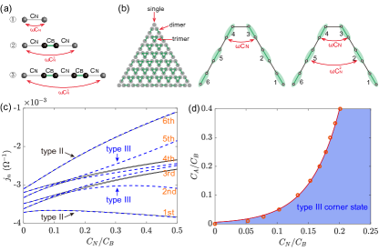
As shown in Fig. 10(b), one can separate the nodes of the breathing kagome lattice into three types: single, dimer, and trimer. The edge spectra are formed by the boundary dimers. Then, we reduce to the effective one-dimensional problem with two edges (green sectors) meeting at the corner, as shown in Fig. 10(b). The effective hopping term connects the 3rd node to the 4th node, and as a result, the 1st and 6th bands split from the edge state continuum and form the type-II corner state [see black line in Fig. 10(c)]. To explain the energy splitting of the type-III corner state, we consider the interaction between the 2nd and 5th, and the result is plotted in Fig. 10(c). We find the 2nd and 5th blue spectrums first submerge in the edge spectrums and then diverge from them at a critical point, and result in the emergence of the type-III corner states. Therefore, a threshold exists for the appearance of type-III corner states, as labeled by the orange dot in Fig. 9(d). In Fig. 10(d), we plot the critical points of emergence of type-III corner state for different capacitance , and one can find the type-III corner state in the blue region. The critical points can be fitted by the following curve
| (21) |
and different gives different threshold . Furthermore, by taking the effective coupling between 1st and 6th nodes into account, we find the 3rd and 4th can deviate from the edge state continuum a little but cannot escape from them. Therefore, one can only observe two types of corner states splitting from the edge spectrums in the present model.
Appendix E The realization of the negative resistance
As shown in Figs. 4(d) and 4(e), the negative resistance is realized by an integrated operational amplifier XL5532 and three resistances , and .
For an ideal operational amplitude, , , and (most modern amplifiers have large gains and input impedances, so the analysis is feasible in a real circuit). According to Ohm’s law, we obtain
| (22) | ||||
Combining these two equations, we have
| (23) |
Here, we choose k, so the network is equivalent to a negative resistance due to .
References
- (1) A. Campa, T. Dauxois, and S. Ruffo, Statistical mechanics and dynamics of solvable models with long-range interactions, Phys. Rep. 480, 57 (2009).
- (2) R. H. French, V. A. Parsegian, R. Podgornik, R. F. Rajter, A. Jagota, J. Luo, D. Asthagiri, M. K. Chaudhury, Y. Chiang, S. Granick, S. Kalinin, M. Kardar, R. Kjellander, D. C. Langreth, J. Lewis, S. Lustig, D. Wesolowski, J. S. Wettlaufer, W.-Y. Ching, M. Finnis, F. Houlihan, O. A. v. Lilienfeld, C. J. v. Oss, and T. Zemb, Long range interactions in nanoscale science, Rev. Mod. Phys. 82, 1887 (2010).
- (3) C. N. Varney, K. Sun, M. Rigol, and V. Galitski, Interaction effects and quantum phase transitions in topological insulators, Phys. Rev. B 82, 115125 (2010).
- (4) W. Beugeling, J. C. Everts, and C. M. Smith, Topological phase transitions driven by next-nearest-neighbor hopping in two-dimensional lattices, Phys. Rev. B 86, 195129 (2012).
- (5) M. Li, D. Zhirihin, M. Gorlach, X. Ni, D. Filonov, A. Slobozhanyuk, A. Alù, and A. B. Khanikaev, Higher-order topological states in photonic kagome crystals with long-range interactions, Nat. Photonics 14, 89 (2019).
- (6) S. Shen, C. Li, and J.-F. Wu, Investigation of corner states in second-order photonic topological insulator, Opt. Express 29, 24045 (2021).
- (7) N. A. Olekhno, A. D. Rozenblit, V. I. Kachin, A. A. Dmitriev, O. I. Burmistrov, P. S. Seregin, D. V. Zhirihin, and M. A. Gorlach, Experimental realization of topological corner states in long-range-coupled electrical circuits, Phys. Rev. B 105, L081107 (2022).
- (8) X.-L. Yu, L. Huang, and J. Wu, From a normal insulator to a topological insulator in plumbene, Phys. Rev. B 95, 125113 (2017).
- (9) D. Leykam, S. Mittal, M. Hafezi, and Y. D. Chong, Reconfigurable Topological Phases in Next-Nearest-Neighbor Coupled Resonator Lattices, Phys. Rev. Lett. 121, 023901 (2018).
- (10) A. W. Sandvik, Ground states of a frustrated quantum spin chain with long-range interactions, Phys. Rev. Lett. 104, 137204 (2010).
- (11) J. W. Britton, B. C. Sawyer, A. C. Keith, C.-C. J. Wang, J. K. Freericks, H. Uys, M. J. Biercuk, and J. J. Bollinger, Engineered two-dimensional Ising interactions in a trapped-ion quantum simulator with hundreds of spins, Nature 484, 489 (2012).
- (12) N. Jia, O. Clai, S. Ariel, S. David, and S. Jonathan, Time- and Site-Resolved Dynamics in a Topological Circuit, Phys. Rev. X 5, 021031 (2015).
- (13) V. V. Albert, L. I. Glazman, and L. Jiang, Topological Properties of Linear Circuit Lattices, Phys. Rev. Lett. 114, 173902 (2015).
- (14) S. Imhof, C. Berger, F. Bayer, J. Brehm, L. W. Molenkamp, T. Kiessling, F. Schindler, C. H. Lee, M. Greiter, T. Neupert, and R. Thomale, Topolectrical-circuit realization of topological corner modes, Nat. Phys. 14, 925 (2018).
- (15) M. Ezawa, Higher-order topological electric circuits and topological corner resonance on the breathing kagome andpyrochlore lattices, Phys. Rev. B 98, 201402 (2018).
- (16) C. H. Lee, S. Imhof, C. Berger, F. Bayer, J. Brehm, L. W. Molenkamp, T. Kiessling, and R. Thomale, Topolectrical Circuits, Commun. Phys. 1, 39 (2018).
- (17) Y. Hadad, J. C. Soric, A. B. Khanikaev, and A. Alù, Self-induced topological protection in nonlinear circuit arrays, Nat. Electron. 1, 178 (2018).
- (18) T. Hofmann, T. Helbig, C. H. Lee, M. Greiter, and R. Thomale, Chiral Voltage Propagation and Calibration in a Topolectrical Chern Circuit, Phys. Rev. Lett. 122, 247702 (2019).
- (19) J. Bao, D. Zou, W. Zhang, W. He, H. Sun, and X. Zhang, Topoelectrical circuit octupole insulator with topologically protected corner states, Phys. Rev. B 100, 201406(R) (2019).
- (20) W. Zhang, D. Zou, J. Bao, W. He, Q. Pei, H. Sun, and X. Zhang, Topolectrical-circuit realization of a four-dimensional hexadecapole insulator, Phys. Rev. B 102, 100102(R) (2020).
- (21) T. Helbig, T. Hofmann, S. Imhof, M. Abdelghany, T. Kiessling, L. W. Molenkamp, C. H. Lee, A. Szameit, M. Greiter, and R. Thomale, Generalized bulk-boundary correspondence in non-Hermitian topolectrical circuits, Nat. Phys. 16, 747 (2020).
- (22) S. Liu, S. Ma, C. Yang, L. Zhang, W. Gao, Y. J. Xiang, T. J. Cui, and S. Zhang, Gain- and Loss-Induced Topological Insulating Phase in a Non-Hermitian Electrical Circuit, Phys. Rev. Applied 13, 014047 (2020).
- (23) N. A. Olekhno, E. I. Kretov, A. A. Stepanenko, P. A. Ivanova, V. V. Yaroshenko, E. M. Puhtina, D. S. Filonov, B. Cappello, L. Matekovits, and M. A. Gorlach, Topological edge states of interacting photon pairs emulated in a topolectrical circuit, Nat. Commun. 11, 1436 (2020).
- (24) L. Song, H. Yang, Y. Cao, and P. Yan, Realization of the Square-Root Higher-Order Topological Insulator in Electric Circuits, Nano. Lett. 20, 7566 (2020).
- (25) H. Yang, Z. X. Li, Y. Liu, Y. Cao, and P. Yan, Observation of symmetry-protected zero modes in topolectrical circuits, Phys. Rev. Res. 2, 022028(R) (2020).
- (26) R. Chen, C.-Z. Chen, J. Gao, B. Zhou, and D.-H. Xu, Higher-Order Topological Insulators in Quasicrystals, Phys. Rev. Lett. 124, 036803 (2020).
- (27) S. Liu, S. Ma, Q. Zhang, L. Zhang, C. Yang, O. You, W. Gao, Y. Xiang, T. J. Cui, and S. Zhang, Octupole corner state in a three-dimensional topological circuit, Light: Sci. Appl. 9, 145 (2020).
- (28) X.-X. Zhang and M. Franz, Non-Hermitian Exceptional Landau Quantization in Electric Circuits, Phys. Rev. Lett. 124, 046401 (2020).
- (29) H. Yang, L. Song, Y. Cao, X. R. Wang, and P. Yan, Experimental observation of edge-dependent quantum pseudospin Hall effect, Phys. Rev. B 104, 235427 (2021).
- (30) Y. Yang, D. Zhu, Z. Hang, and Y. Chong, Observation of antichiral edge states in a circuit lattice, Sci. China Phys. Mech. Astron. 64, 257011 (2021).
- (31) H. Yang, L. Song, Y. Cao, and P. Yan, Experimental Realization of Two-Dimensional Weak Topological Insulators, Nano. Lett. 22, 3125 (2022).
- (32) M. D. Ventra, Y. V. Pershin, and C.-C. Chien, Custodial Chiral Symmetry in a Su-Schrieffer-Heeger Electrical Circuit with Memory, Phys. Rev. Lett. 128, 097701 (2022).
- (33) J. Wu, X. Huang, Y. Yang, W. Deng, J. Lu, W. Deng, and Z. Liu, Non-Hermitian second-order topology induced by resistances in electric circuits, Phys. Rev. B 105, 195127 (2022).
- (34) N. A. Olekhno, A. D. Rozenblit, A. A. Stepanenko, A. A. Dmitriev, D. A. Bobylev, and M. A. Gorlach, Topological transitions driven by quantum statistics and their electrical circuit emulation, Phys. Rev. B 105, 205113 (2022).
- (35) D.-A. Galeano, X.-X. Zhang, and J. Mahecha, Topological circuit of a versatile non-Hermitian quantum system, Sci. China Phys. Mech. Astron. 65, 217211 (2022).
- (36) Q. Pei, W. Zhang, D. Zou, X. Zheng, and X. Zhang, Valley-dependent bilayer circuit networks, Phys. Lett. A 445, 128242 (2022).
- (37) W. Zhang, H. Yuan, H. Wang, F. Di, N. Sun, X. Zheng, H. Sun, and X. Zhang, Observation of Bloch oscillations dominated by effective anyonic particle statistics, Nat. Commun. 13, 2392 (2022).
- (38) W. A. Benalcazar and A. Cerjan, Bound states in the continuum of higher-order topological insulators, Phys. Rev. B 101, 161116(R) (2020).
- (39) Y. Hatsugai and I. Maruyama, topological invariants for Polyacetylene, Kagome and Pyrochlore lattices, EPL 95, 20003 (2011).
- (40) T. Kariyado, T. Morimoto, and Y. Hatsugai, Berry Phases in Symmetry Protected Topological Phases, Phys. Rev. Lett. 120, 247202 (2018).
- (41) K. Kudo, T. Yoshida, and Y. Hatsugai, Higher-Order Topological Mott Insulators, Phys. Rev. Lett. 123, 196402 (2019).
- (42) H. Araki, T. Mizoguchi, and Y. Hatsugai, Berry phase for higher-order symmetry-protected topological phases, Phys. Rev. Res. 2, 012009 (2020).
- (43) Y. Zhang, Y.-W. Tan, H. L. Stormer, and P. Kim, Experimental observation of the quantum Hall effect and Berry’s phase in graphene, Nature 438, 201 (2005).
- (44) T. Ando, Y. Zheng, and H. Suzuura, Dynamical Conductivity and Zero-Mode Anomaly in Honeycomb Lattices, J. Phys. Soc. Jpn. 71, 1318 (2002).
- (45) J. Tworzydlo, B. Trauzettel, M. Titov, A. Rycerz, and C. W. Beenakker, Sub-Poissonian Shot Noise in Graphene, Phys. Rev. Lett. 96, 246802 (2006).
- (46) M. I. Katsnelson, K. S. Novoselov, and A. K. Geim, Chiral tunnelling and the Klein paradox in graphene, Nat. Phys. 2, 620 (2006).
- (47) N. Stander, B. Huard, and D. Goldhaber-Gordon, Evidence for Klein Tunneling in Graphene p-n Junctions, Phys. Rev. Lett. 102, 026807 (2009).
- (48) X. Ni, M. Weiner, A. Alù, and A. B Khanikaev, Observation of higher-order topological acoustic states protected by generalized chiral symmetry, Nat. Mater. 18, 113 (2019).
- (49) M. Janssen, Statistics and scaling in disordered mesoscopic electron systems, Phys. Rep. 295, 1 (1998).
- (50) H. Araki, T. Mizoguchi, and Y. Hatsugai, Phase diagram of a disordered higher-order topological insulator: A machine learning study, Phy. Rev. B 99, 085406 (2019).
- (51) H. Wakao, T. Yoshida, H. Araki, T. Mizoguchi, and Y. Hatsugai, Higher-order topological phases in a spring-mass model on a breathing kagome lattice, Phys. Rev. B 101, 094107 (2020).