Vacancy-related color centers in twodimensional silicon carbide monolayers
Abstract
Basic vacancy defects in twodimensional silicon carbide (2D-SiC) are examined by means of density functional theory calculations to explore their magneto-optical properties as well as their potential in quantum technologies. In particular, the characteristic hyperfine tensors and optical excited states of carbon-vacancy, silicon-vacancy, and carbon antisite-vacancy pair defects in 2D-SiC are determined that are the key fingerprints of these defects that may be observed in electron paramagnetic resonance and photoluminescence experiments, respectively. Besides the fundamental characterization of the most basic native defects, we show that the negatively charged carbon antisite-vacancy defect is a promising candidate for realizing a near-infrared single-photon quantum emitter with spin doublet ground state, where the negative charge state may be provided by nitrogen doping of 2D-SiC. We find that the neutral carbon-vacancy with spin triplet ground state might be used for quantum sensing with a broad emission in the visible.
I Introduction
Point defects in semiconductors and related materials may significantly alter the host material’s electrical, optical, and magnetic properties. In traditional semiconductors, shallow-level point defects may be used as dopants to deliberately introduce carriers. In contrast, deep-level point defects act as carrier traps or recombination centers that can deteriorate the operation of semiconductor devices. Recently, this negative view about deep-level point defects has been radically changed after a room temperature electron spin resonance observation of a single point defect by optical means which was demonstrated for the negatively charged nitrogen-vacancy (NV) defect in diamond Gruber et al. (1997); Doherty et al. (2013); Gali (2019). As the emission came from a single defect, it acted as a single-photon source or quantum emitter. The coherent manipulation, initialization, and readout of a single defect spin is a realization of a solid-state defect quantum bit or qubit that can be employed in quantum sensing, simulation, computation, and entanglement-based quantum communication studies and applications (e.g., Ref. Wolfowicz et al., 2021).
The success of the diamond NV center has motivated researchers to seek alternative paramagnetic quantum emitters that may have favorable magneto-optical or spin-coherence properties in technologically more mature materials than diamond, e.g., the threedimensional (3D) silicon carbide (SiC) Gali et al. (2010); Weber et al. (2010); Gali (2011); Koehl et al. (2011); Anderson and Awschalom (2023). Since then, single-photon emitters with or without coherent manipulation of electron spins have been found in various materials, including twodimensional (2D) ones Zhang et al. (2020a); Montblanch et al. (2023). The platforms offered by 2D materials have certain crucial advantages as compared to their bulk counterparts in 3D materials: they typically have very high extraction efficiency with avoiding total internal reflection and can be well integrated with cavities and photonic waveguides and coupled to plasmonic structures Aharonovich et al. (2016).
The first 2D material discovered Novoselov et al. (2004), namely graphene, is a zero band gap material that cannot host single-photon emitters. Changing the chemical composition is one possible route to open the gap in carbon-based 2D materials. For example, every second carbon atom in graphene may be replaced by a silicon atom to produce a honeycomb-structured SiC material Lin et al. (2015); Susi et al. (2017) that we label by 2D-SiC in the context. This material should produce a band gap because of the partial polarization of the covalent bonds between carbon and silicon atoms and the breaking of the high symmetry of graphene as confirmed by first principles calculations at various levels of theory Bekaroglu et al. (2010); Hsueh et al. (2011); Susi et al. (2017); Hassanzada et al. (2020).
Very recently, the synthesis of this semiconductor material has been reported Chabi et al. (2021); Polley et al. (2023). Optical signals have been observed at room temperature for the 2D-SiC nanoflakes Chabi et al. (2021). In the absorption spectrum, two high intensity peaks were found with a maximum intensity at approximately 2.2 eV and 2.5 eV with a smaller peak at around 2.3 eV. In the photoluminescence spectrum, 1.0 eV-broad intense peak was found with a Gaussian shape where the maximum of the peak is located at around 2.58 eV Chabi et al. (2021). They associated this PL peak with the band edge emission based on the common appearance of intense peaks in the photoluminescence (excitation at 420 nm) and the absorption at around 2.6 eV in the same 2D-SiC nanoflakes sample. In a forthcoming experimental study, the 2D phase of SiC was found to be almost planar and stable at high temperatures up to 1200 ∘C in vacuum Polley et al. (2023). The stability of 2D-SiC was previously predicted by density functional theory (DFT) calculations that showed all the phonon frequencies to be positive in the Brillouin zone (BZ) in its planar geometry Bekaroglu et al. (2010). As the existence and stability of this material have been recently demonstrated in experiments Polley et al. (2023), it can be considered as an interesting 2D platform to host quantum emitters and qubits.
Recent advances in first principles techniques have made them highly predictive to explore potential defect qubit candidates Gali (2019); Zhang et al. (2020a); Gali (2023). In our previous work, we carried out DFT calculations with a focus on Stone-Wales-related defects Hassanzada et al. (2020) to this end. On the other hand, many color centers in 3D and 2D materials are vacancy-like and can be created either during growth or by irradiation techniques Zhang et al. (2020a). We note that the isolated single silicon-vacancy in 3D forms of SiC has been proven to be room temperature qubits Riedel et al. (2012); Widmann et al. (2015); Zhang et al. (2020a); Soykal et al. (2016), thus one might expect similar results in 2D-SiC. Furthermore, the magneto-optical characterization of the basic vacancy defects in 2D-SiC is fundamental to gain insight into the properties of real 2D-SiC materials. These issues motivated us for a detailed study of vacancy-type defects in 2D-SiC.
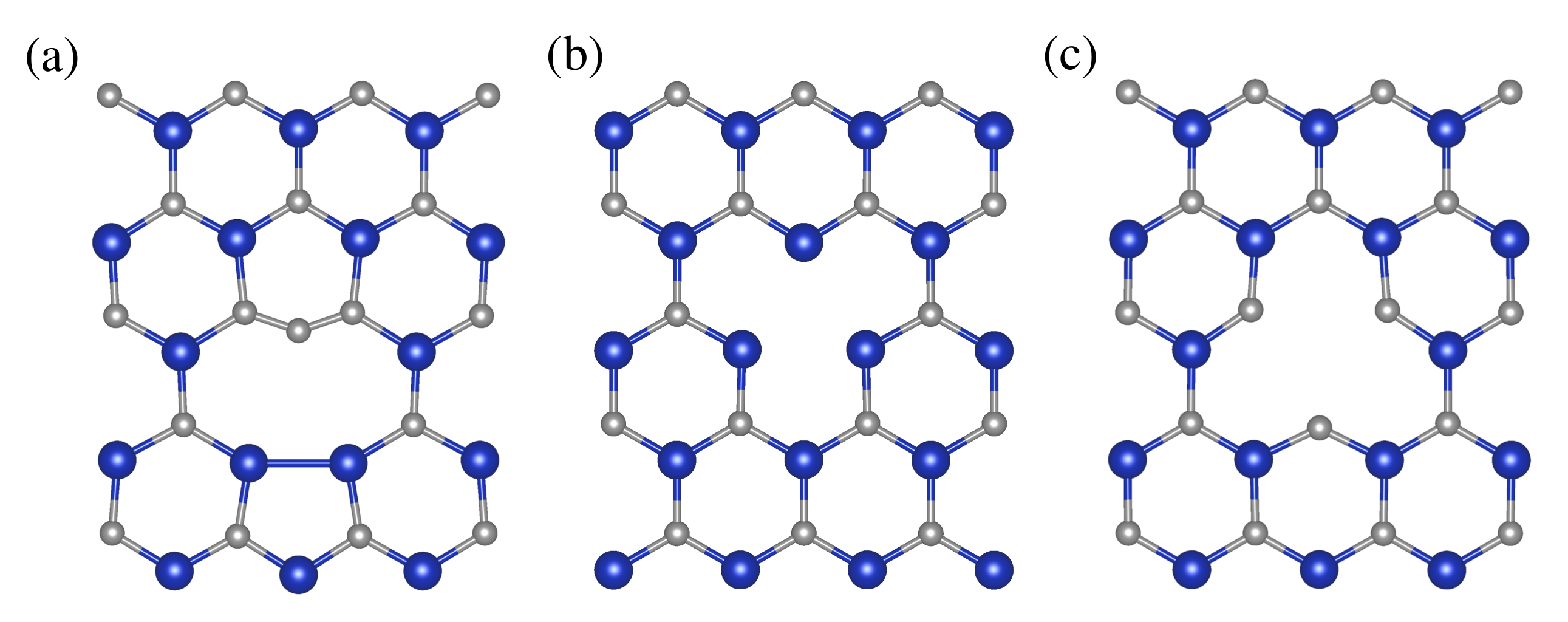
In 2D-SiC lattice, all the carbon and silicon atoms are equivalent by symmetry, thus the two simplest vacancy defects are the isolated carbon-vacancy (V) and silicon-vacancy (V). We learnt from 3D-SiC Rauls et al. (2000); Bockstedte et al. (2003); Umeda et al. (2007); Deák et al. (2011); Castelletto et al. (2014a, b) that V has another atomic configuration when one of the neighboring carbon atoms near the vacant site jumps to the vacancy by creating a carbon antisite-vacancy pair defect denoted by V-C. The structures of these basic vacancy defects are depicted in Fig. 1. The optical properties of these defects in part have been previously studied modeled in a small supercell Hassanzada et al. (2020) but a detailed magneto-optical characterization for these important defects is still lacking. Here, we apply advanced plane-wave supercell DFT calculations to compute the electronic structure, formation energies, photoionization thresholds, electron spin resonance hyperfine parameters, and the basic optical parameters of these defects. Furthermore, we simulate the photoluminescence spectrum for the most relevant defects. Our results provide a reference for future electron spin resonance and photoluminescence studies of 2D-SiC. We find that the negatively charged V-C defect is a good candidate to operate as a near-infrared quantum emitter and may be used to realize a qubit in 2D-SiC. Furthermore, the carbon-vacancy has a triplet ground state with a broad emission in the visible that might be harnessed as a quantum sensor if optically detected magnetic resonance is confirmed for the defect.
II Method
In this work, we employ plane-wave supercell DFT calculations Kohn and Sham (1965); Hohenberg and Kohn (1964) with the projector-augmented-wave (PAW) method Blöchl (1994); Kresse and Joubert (1999) as implemented in the Vienna Ab-initio Simulation Package (VASP) Kresse and Furthmüller (1996, 1996). The exchange-correlation functional of Heyd, Scuseria, and Ernzerhof Heyd et al. (2003) was used with its parameters set to standard values (HSE06). For all unit cell calculations, a dense -centered -point mesh of was used, while supercell calculations were performed using a single point. The geometry was optimized with the criterion of 10-2 eV/Å per atom for the Hellman-Feynman forces and a kinetic energy cutoff of 450 eV was used. We employed a vacuum region of 12 Å and 24 Å in the direction for the and supercells, respectively, minimizing all interactions between periodic images of the embedded defects. The SCF method Gali et al. (2009) was implemented in VASP to calculate the electronic excited state with optimizing the geometry in the excited state where all the atoms are allowed to relax in the geometry optimization procedure. After geometry optimization the zero-phonon-line energies can be calculated and the obtained geometry in the electronic excited state also contributes to the simulation of the phonon sideband of the photoluminescence spectrum as will be explained below.
The equilibrium geometry in the electronic ground and excited states may differ. The difference in the geometries of the electronic ground and excited states () may be defined Alkauskas et al. (2012) as
| (1) |
where indicates the atom index, , is the atomic mass of species and is the position of atom in the ground ()/excited () state. Usually, the larger the difference the larger the phonon sideband in the photoluminescence spectrum for the optically allowed transition.
For the calculation of phonon frequencies and normal coordinates, we used the same parameters as above for the vacuum region, cutoff energy, and -point sampling. However, the more traditional functional of Perdew, Burke, and Ernzerhof (PBE) Perdew et al. (1996) was applied to optimize the forces on each atom within a threshold of 10-3 eV/Å. The phonons were calculated in the electronic ground state by DFT perturbation theory as implemented in VASP. Choosing the exchange-correlation functional of PBE over HSE06 in our phonon calculations provides reasonably accurate results while significantly reducing the computational time.
The photoluminescence spectrum of the emitters may reveal their potential in various quantum technology applications. In quantum communication applications, the coherent emission only comes at the no-phonon or zero-phonon-line (ZPL) emission. The fraction of ZPL and total emission can be observed in experiments from the Debye-Waller factor (). In the theoretical simulation of the emitters, the Huang-Rhys (HR) theory may be applied to calculate the phonon sideband of the photoluminescence spectrum Alkauskas et al. (2014); Thiering and Gali (2018) which requires the optimized geometries in the ground and optical excited states as well as the phonons in the ground state. The total Huang-Rhys factor () indicates in the HR theory how many effective phonons participate in the optical transition and it is related to by
| (2) |
To calculate the phonon sideband of the spectrum, the partial HR factors should be calculated as explained in Ref. Alkauskas et al., 2014. The partial Huang-Rhys factor is where is defined as in Eq. (1) but should be replaced by the coordinates of ions associated with the normal coordinate of the phonon. The temperature-dependent spectrum can be calculated by the Fourier transform of the partial HR factor as
| (3) |
where is the Bose-Einstein distribution function,
| (4) |
where is the Boltzmann-constant and is temperature.
The phonon sideband of the spectrum can then be defined as
| (5) |
where is a normalization constant and is the broadening of the ZPL emission. We apply HR theory to calculate the HR factors and the shape of the phonon sideband of the photoluminescence spectrum. We note that we applied HSE06 optimized geometries and PBE phonons in this procedure using an in-house code. This approach produced an accurate optical spectrum for defects in diamond and 3D-SiC Thiering and Gali (2017, 2018); Csóré et al. (2022a, b). We further note that the temperature broadening of the ZPL emission or complicated anharmonicity and renormalization related effects are not considered in the simulation of temperature broadening in the optical spectrum which goes beyond the scope of our study.
For the paramagnetic defects, we determined the key magnetic parameters that may be observed by electron spin resonance techniques. For ensemble defect measurements, the statistics of the nuclear spin distribution proximate to the defect and the electron spin density distribution will produce a unique fingerprint caused by the hyperfine interaction. Therefore, the electron paramagnetic resonance (EPR) spectrum is a powerful method to identify the atomic structure of the defect, in particular, when combined with the DFT simulated spectra. The shape of the EPR spectrum is mostly set by the hyperfine (HF) tensor of the nuclear spins which is given by
| (6) |
where is the spin density of spin state at the site , is the electron Bohr magneton and is the nuclear Bohr magneton for nucleus , whereas refers here to the unit vector of . The first and second terms in the parentheses represent the Fermi-contact and dipole-dipole terms, respectively. The dominance of the Fermi-contact term over the dipole-dipole one will produce a characteristic hyperfine sideband in the EPR spectrum as the Fermi-contact term strongly depends on the spin density localized at the nucleus. We note that Eq. (6) is modified within the PAW formalism Blöchl (2000), and the spin polarization of the core orbitals is taken into account for accurate HSE06 calculations Szász et al. (2013).
The EPR spectrum of high-spin () defects may be further modified even in the absence of an external magnetic field, due to the electron spin-spin dipole interaction. The so-called zero-field-splitting (ZFS) can be described by the Hamiltonian operator
| (7) |
where is the vector between the spins, is the spin operator vector, is the Bohr magnet on of the electron, and is the magnetic permeability of vacuum. The formula in Eq. (7) can be cast to
| (8) |
where S is the total spin vector and D is zero-field-splitting tensor (ZFST). Since the eigenvalue framework matrix is diagonal, the spin-spin Hamiltonian can be expressed as
| (9) | ||||
| (10) |
where are the components of the ZFST, with are the spin matrices, are the spin raising and lowering operators, , and and are the two parameters of the ZFST in the eigenvalue framework. The parameters and can be expressed as
| (11) |
where is the axial parameter whereas is the orthorhombic parameter, so the latter is non-zero for defects with low symmetries. We consider the electron spin dipole-dipole interaction as a source of ZFS which is calculated as was implemented by Martijn Marsman in VASP within the PAW formalism Rayson and Briddon (2008); Bodrog and Gali (2013); Ivády et al. (2018).
As we will note below, a strongly correlated electronic structure could develop in certain cases which is manifested as symmetry breaking solution for the Kohn-Sham wavefunctions in the spinpolarized hybrid DFT calculations. This solution may yield a proper total energy of the system but it is improper for the spin density or spin density matrix related quantities. To approximate the HF tensor and ZFST for these cases, we constrained the Kohn-Sham wavefunctions to reflect the symmetry of the system. This procedure was successfully applied to oxygen defects in diamond Thiering and Gali (2016).
III Results
We investigate vacancy defects in a self-standing monolayer of 2D-SiC. We first briefly describe the host 2D-SiC system and then turn to the basic electronic structure of the vacancy defects. We define the formation energies of the defects which reveal their relative stability, charge transition levels, and photoionization thresholds. We then determine the ground-state spin properties of the paramagnetic vacancy defects. Finally, we compute and discuss their optical properties in detail by providing the photoluminescence spectrum for the most relevant vacancy defects. In the discussion, we also show results for the n-type doping of 2D-SiC in the context.
The pristine 2D-SiC crystal is optimized using HSE06 which yields a lattice constant of Å and Si-C bond length of 1.77 Å, which agree well with the experimental data at 3.1 Å and 1.79 Å (Ref. Chabi et al., 2021), respectively. The calculated band gap is 3.58 eV, which broadly agrees with previous calculations at various levels of theory Hassanzada et al. (2020); Hsueh et al. (2011). After optimizing the local 2D-SiC structure, we construct monolayer supercells and embed the three vacancy defects as depicted in Fig. 1.
III.1 Electronic structure of the vacancy defects
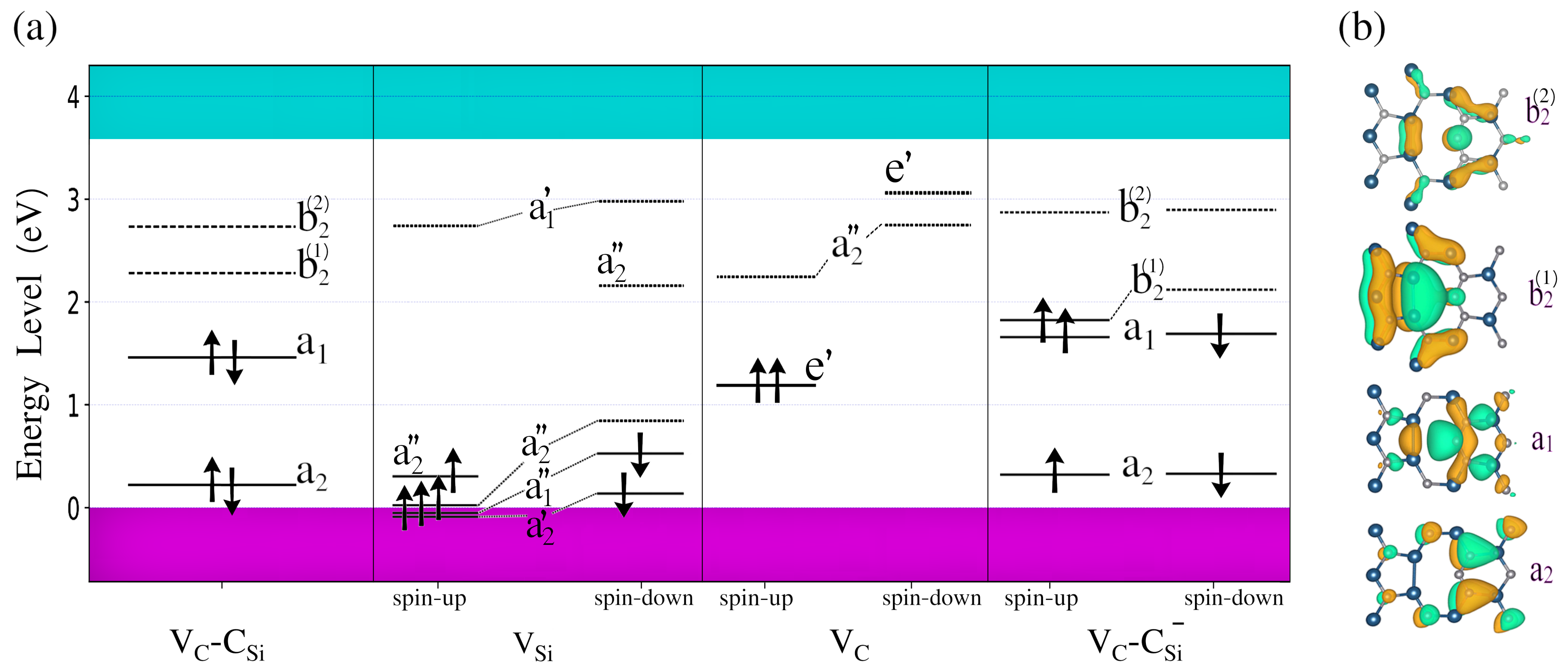
The neutral vacancy defects have dangling bonds that introduce occupied and empty defect levels in the fundamental band gap as depicted in Fig. 2 and labeled by the irreducible representation of the associated point group as given in Fig. 1. We illustrate the symmetry of the Kohn-Sham wave functions on the V-C defect in Fig. 2(b). The V and V defects have high-spin ground state with D3h symmetry in the spinpolarized HSE06 calculations. We note that the spinpolarized hybrid DFT solution exhibits symmetry for the Kohn-Sham wavefunction of V which is the signature of highly correlated state and the possibility that the true ground state of the system could be a highly correlated singlet state, similar to the neutral silicon-vacancy in 3D-SiC Deák et al. (1999). This means that the total energy of this state is less accurately calculated than the non-highly correlated ones, and the true spin state of the electronic ground state is uncertain. Nevertheless, the triplet state may be observed at elevated temperatures, thus we further consider this high-spin state for V.
We find that all the considered defects contain filled and empty levels in the gap. This implies that all the defects may be ionized by varying the position of the Fermi-level in the band gap. To determine the stability of the ionized defects the formation energy of the defects is computed which also reveals the relative stability of these defects in thermal equilibrium. In the next section, the details about the calculations of the formation energy of defects are described which is followed by the HSE06 results.
III.2 Formation energies, relative stability, charge transition levels, doping, and photoionization thresholds
The stability of the defect structures is determined via the formation energy. For a defect in charge state , the formation energy () is given by Zhang and Northrup (1991); Komsa et al. (2012),
| (12) | ||||
which depends on the Fermi-level energy . The energies are referenced to the calculated valence band maximum (VBM) of the perfect supercell. The quantities and are the total energy of the defected system and the finite-size electrostatic correction, respectively, both representing the charge state . is the alignment between the electrostatic potentials of the pristine and defective supercells. The term is the total energy of a pristine supercell of the same size. The parameter refers to the number of atoms of type added (positive) or removed (negative) from the perfect crystal with the appropriate chemical potential .
The electrostatic corrections are calculated within the spirit of Freysoldt-Neugebauer-van de Walle (FNV) method Freysoldt et al. (2009) as implemented in the software package CoFFEE Naik and Jain (2018) which goes as
| (13) |
where is the long-range interaction energy which is obtained by solving the Poisson equation with using a model charge distribution and a model dielectric profile . is given by
| (14) |
where the integral is over the supercell volume . The quantity is evaluated for larger supercells and extrapolated to obtain . gives the DFT difference electrostatic potential to the model potential as
| (15) |
where the planar-averaged electrostatic potentials are obtained along the direction. We apply this charge correction scheme to the special excited state of the neutral defects which can be described by defect level to band edge transition in order to account for the supercell size correction of this special excited state (see Refs. Zhang et al., 2020b; Udvarhelyi et al., 2022; Gali, 2023). The charge correction in the total energy of V-C, V and V defects in their positive and negative charge states is around eV in our supercell.
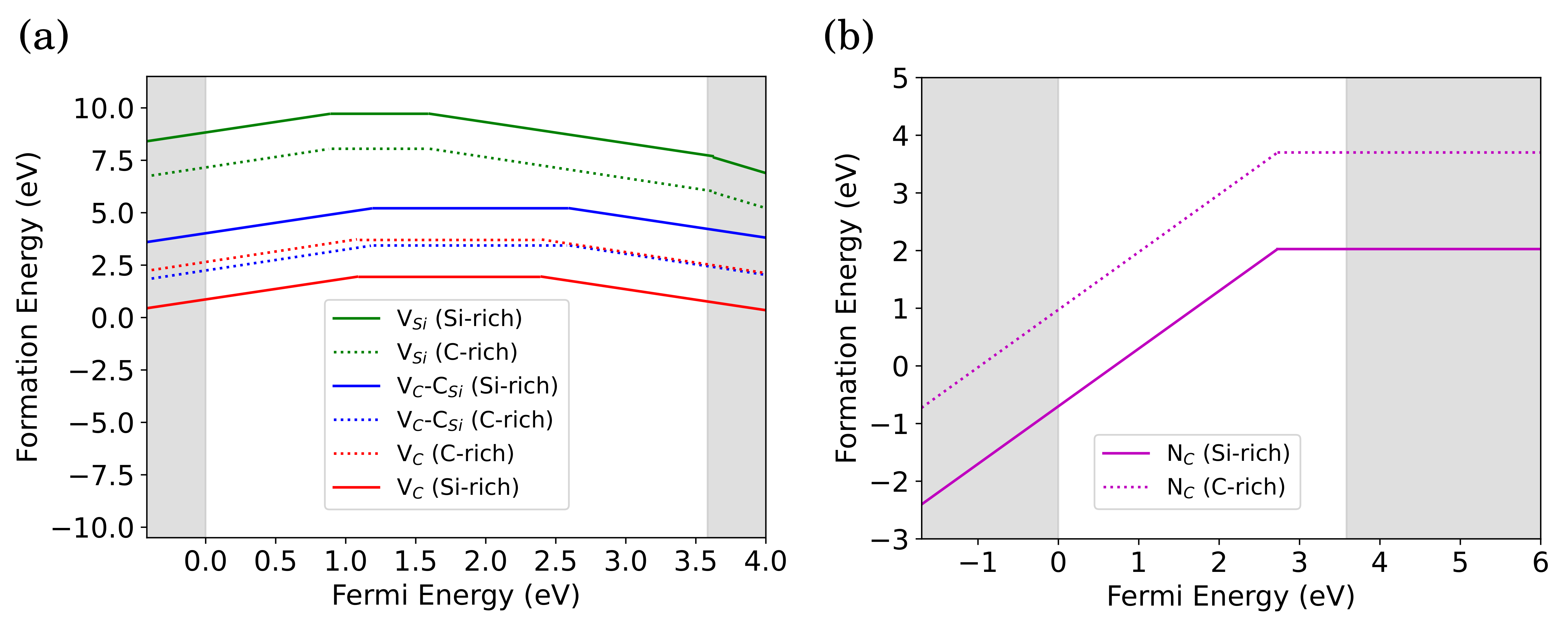
When computing the formation energy, different growth conditions have to be taken into account. The two extreme growth conditions for the 2D-SiC binary compound correspond to Si-rich and C-rich ones. When including these conditions into the formation energy, the chemical potential must be evaluated under such conditions. In the Si-rich case, is calculated from a silicon crystal. The term is then taken from the equilibrium condition
| (16) |
where is the chemical potential of the 2D-SiC primitive cell. In C-rich condition, is taken from the diamond crystal and is determined again with Eq. (16). The formation energies of V-C, V-C, and V are then computed using Eq. (12).
The results are plotted in Fig. 3(a) for both Si-rich and C-rich conditions. The crossing points in the plot for a given defect show the charge transition levels that are listed in Table 1. The and charge transition levels for the V-C, V and V defects in Fig. 3(a) appears deep in the fundamental band gap. In particular, the and charge transition levels appear at eV and eV for V-C, eV and eV for V, and eV and eV for V, respectively. We checked that the double negative charge state is unstable for V-C, V and V defects.
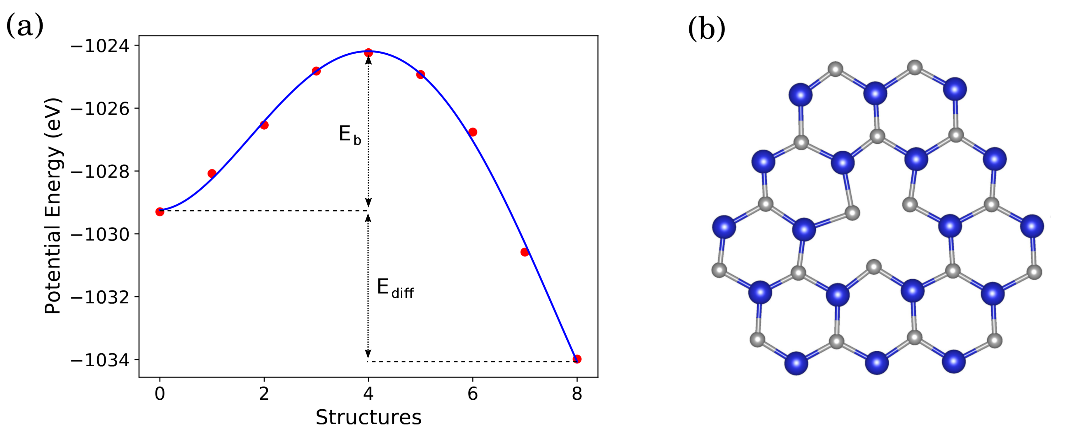
We find that the V defect is the most stable basic vacancy-type defects in 2D-SiC which is followed by the V-C defect in hierarchy. Our calculations imply that V is significantly less stable than its twin counterpart V-C, irrespective to the position of the Fermi-level. This might indicate that V does not occur in 2D-SiC. However, V might form by irradiation techniques that can further survive as a metastable defect. Indeed, we find that the barrier energy of the transformation from V to V-C is 4.96 eV (see Fig. 4) as obtained by nudged elastic band method Henkelman et al. (2000) which is very high and should be stable even at high-temperature annealing. As a consequence, the properties V defects are further considered in the context. We further note that if the V defect becomes mobile at a certain annealing temperature then it may be combined with an existing C defect which has relatively low formation energy at 4.43 eV in Si-rich condition. In that case, additional V-C defects may be created by complex formation. We find that the complex formation is favored by eV in the neutral charge state (when the Fermi-level is pinned to the middle of the gap).
In order to stabilize the acceptor states of the vacancy defects in thermal equilibrium, donors should be introduced into 2D-SiC. It has been shown in SiC nanotubes Gali (2006) that nitrogen-substituting carbon behaves as a donor. SiC nanotubes can be considered as tubular forms of SiC sheets, thus this idea may be transferable to 2D-SiC. We considered nitrogen substituting carbon, N, as a donor candidate in 2D-SiC. In order to calculate its formation energy, the chemical potential of nitrogen should be known in Eq. (12). To this end, we considered the most stable structure of the hexagonal Si3N4 crystal with a space group. Si3N4 acts as the second phase that can determine the solubility limit. It is chosen because it is the most stable structure that can form between nitrogen and either silicon or carbon, hence giving us the limits for when nitrogen is introduced to the system. Thus, the chemical potential of nitrogen () can be defined as
| (17) |
where is the chemical potential of the hexagonal Si3N4 primitive cell and can vary between the Si-rich and C-rich conditions as set above. We find that NC is, in fact, a donor in 2D-SiC with level at eV or eV (where CBM refers to a conduction band minimum) as shown in Fig. 3(b). The formation energy of N is low; thus it is likely that N doped 2D-SiC can support negatively charged vacancy defects.
| Defect | (eV) | (eV) | (eV) |
|---|---|---|---|
| V | 0.9 | 1.6 | 3.6 |
| V-C | 1.2 | 2.6 | 4.8 |
| V | 1.1 | 2.4 | 4.9 |
| N | 2.7 |
Another way to realize a given charge state of the defect is photoionization upon illumination which is not a thermal equilibrium process. By laser irradiation with energy above the ionization threshold, a defect can be driven to a photoionized charge state. Although, photoionization may be harmful to the realization of a stable emission from a given defect when it drives out the defect from its target charge state, leading to blinking or permanent quenching. The photoionization threshold energies may be lower than the neutral excitation energies of the defect in a given charge state, so then photoionization can be avoided, at least, in the regime of linear optical excitation. The photoionization threshold energies of the vacancy defects can be read out in Fig. 3(a). We illustrate the role of photoionization in the relevant V-C defect with level at eV. Assuming that the defect was in the negative charge state, an electron may be promoted from the occupied defect level to the conduction band by a eV excitation energy. Thus, the condition of the existing photoluminescence signal from the negatively charged V-C is that the associated optical excitation energies should be smaller than 0.98 eV. Using the same argument, these values are 1.98 eV for the single negative charge state of V and 1.18 eV for the single negative charge state of V, respectively. For the complete picture, one has to consider the deep donor levels of the defects, too. If the defects were in their neutral charge state then the value of occupation level with respect to the conduction band minimum provides photoionization thresholds when the electron is promoted from the in-gap defect level to the conduction band edge. As an example, the neutral carbon-vacancy, V, has such photoionization threshold at eV. However, there is a lower ionization threshold at around 2.40 eV which transforms V to V. This is a typical amphoteric defect where both the electrons and holes may be generated by illumination or captured in the dark by the defect. However, once we arrive at the negative charge state by photoexcitation with laser energy higher than 2.4 eV then the next photon will turn V to V because the ionization threshold of this process is at around eV. If the laser energy is higher than 2.48 eV then the defect may be ionized to V. However, the next photon would bring it back again to V because the ionization threshold of this process is just 1.1 eV. The conclusion is that the defect dynamically stays in the neutral charge state upon laser illumination even at high-energy illumination ( eV) and it definitely stays there when the excitation energy is just below the photoionization threshold energy. A similar scenario can be drawn for the neutral V-C too.
III.3 Electron spin resonance parameters
| Defect, spin | Atoms | (MHz) | (MHz) | (MHz) |
|---|---|---|---|---|
| V, 1/2 | C1-C2C6 | 38.4 | 35.3 | 49.0 |
| Si1-Si2-Si3 | ||||
| V, 1 | C1-C2C6 | |||
| Si1-Si2-Si3 | ||||
| V, 3/2 | C1-C2C6 | |||
| Si1-Si2-Si3 | ||||
| V-C, 1/2 | C1 | |||
| C2-C3 | ||||
| Si1-Si2 | ||||
| Si3-Si4 | ||||
| V-C, 1/2 | C1 | |||
| C2-C3 | ||||
| C4-C5 | ||||
| Si4-Si5 | ||||
| Si1-Si2 | ||||
| Si3 | ||||
| V, 3/2 | C1-C2-C3 | 122.5 | 116.1 | 200.5 |
| V, 1 | C1-C2-C3 | 86.3 | 56.3 | 97.7 |
| V, 1/2 | C1-C2-C3 | 127.1 | 123.6 | 204.3 |
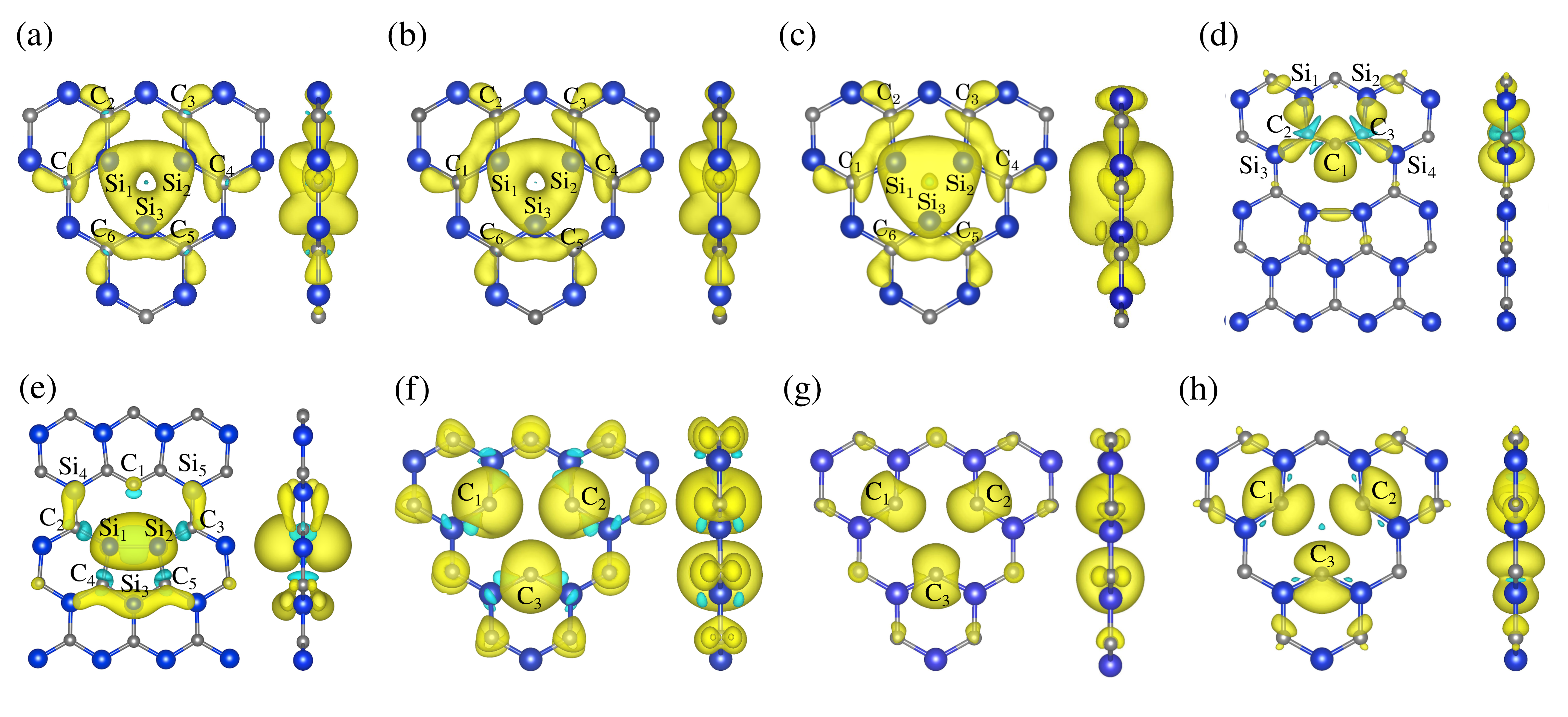
Most of the considered vacancy defects have a paramagnetic ground state or low-energy metastable state. The respective spin density distributions are displayed in Fig. 5. These defects may be observed by electron spin resonance techniques. 2D-SiC consists of 13C and 29Si nuclear spins with about 1.1% and 4.5% natural abundance; a hyperfine interaction may be developed between the electron spin and the nuclear spins that are randomly distributed in the 2D-SiC crystal. These hyperfine interactions provide an unique pattern in their electron spin resonance spectrum that could be an important fingerprint for identification. The most important atomic positions around the vacancies are labeled in Fig. 5. The hyperfine interaction can be fully described by the hyperfine (HF) tensor as explained in Sec. II. The calculated HF tensor can be diagonalized yielding the three principal values, also known as the HF constants. The HF constants are labeled as , , and , and following standard convention the largest absolute value is associated with . We find that the spin density of V, V, V and V shows symmetry breaking solution which is a sign of multi-determinant nature in the ground state. We reiterate here that to estimate the hyperfine and zero field interactions for these cases, we symmetrized the Kohn-Sham wavefunctions so the spin density according to the point group symmetry of the geometry as depicted in Fig. 5.
In V, the spin density is predominantly localized on the nearest Si atoms labeled as Si1, Si2, and Si3 as expected because the dangling bonds of these three Si-atoms produce the orbitals in the band gap. The average HF constant for these three 29Si isotopes is MHz. The V and V defects produce very similar spin density distribution to the neutral one with the average HF constant of MHz and MHz, respectively.
In the V-C defect, the spin density is mainly localized on the Si1 and Si2 atoms, leading to an average HF constant of about MHz. On the other hand V-C defect has mostly localized spin density on the Si1 and Si2 atoms with an average HF constant of about MHz and at C1 atom it is about MHz.
In V defect, the carbon dangling bonds introduce the spin densities. As a consequence, the spin density is mostly localized on C1, C2, and C3 ions for V, V and V defects (Table 2 and Fig. 5) with an average HF constant of MHz, MHz and MHz, respectively.
Next, we calculate the ZFS parameters for high-spin defects. For V with spin state, the computed MHz and MHz (cf. Eq. (11)) are surprising for planar defect structures. This can be explained by the large out-of-plane extension of the spin density creating a sphere-like shape, for which the dipolar spin-spin related ZFS vanishes. In some cases, this effect is so enhanced, that the extent of the spin density is more out-of-plane than in-plane, resulting in a negative value. As a consequence, the V with yields MHz and MHz. This phenomenon is only present for the silicon dangling bonds, in line with the preferential sp3 hybridization of the silicon atoms. For V () and V (), MHz and GHz are significant and characteristic, although, they may belong to the metastable state. We reiterate that we forced the high symmetry solution for the Kohn-Sham wavefunctions in order to estimate the ZFS parameters for this defect in its state. We note that the large value for V occurs due to the larger out-of-plane extension of the spin density, in contrast to that of V as depicted in Figs. 5(f) and (g), respectively.
The calculated HF constants for the immediate neighbor atoms of all the three defects are summarized in Table 2. We find that these defects produce very different EPR spectra and can be well identified by electron spin resonance techniques.
III.4 Optical properties: zero-phonon line and phonon sideband of the optical spectrum and the radiative lifetime
| Defect | Transition | (eV) | (nm) | HR | DW (%) | El. conf. | |
|---|---|---|---|---|---|---|---|
| V-C | 0.50 | 2479 | 8.8 | 0.01% | 1.11 | ||
| 1.27 | 976 | 9.41 | 0.008% | 1.17 | |||
| V-C | 0.59 | 2101 | 0.80 | 44% | 0.39 | ||
| V | 2.54 | 629 | 1.88 | 15.26% | 0.57 | ||
| 2.26 | 729 | 6.57 | 0.001% | 1.47 |
Vacancy defects introduce multiple filled and empty defect levels in the fundamental band gap in 2D-SiC. This may lead to visible or near-infrared emission upon photoexcitation below the photoionization threshold energies for the optically allowed transitions. Some of the excited states may have a zero optical transition dipole moment () towards the electronic ground state by symmetry that we call dark states. Although, dark states could fluoresce with the assistance of phonons, the so-called Herzberg-Teller optical transition, we ignore this scenario because the direct non-radiative decay by phonons (internal conversion) could be very competitive, in particular, for the cases where the energy gap between the ground and excited states is less then 0.5 eV.
We find that V defect has a highly correlated electronic structure with very complicated ground and excited states. Here the predictive power of the Kohn-Sham DFT method is questionable so we do not attempt to produce an optical signature for these defects. Nevertheless, we note that the defect is most likely stable in its negative charge state when donors are present in 2D-SiC or can be driven to this charge state by photoexcitation with laser energy at eV. We can estimate the ZPL energy for V from the calculated occupation level with respect to the conduction band edge which yields eV. The photoluminescence spectrum should show a broad emission with a maximum intensity at lower energy than the ZPL energy coming from the phonon-assisted optical transitions because of the large relaxation energy going from the neutral to the negative charge state of the defect.
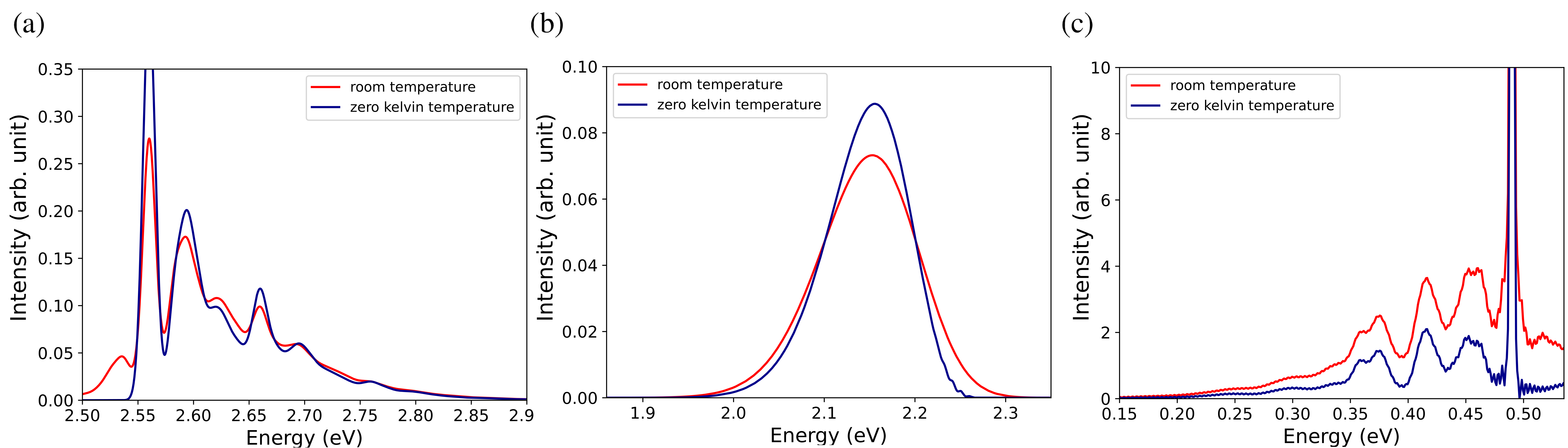
The most stable vacancy defect is V, so we analyze its optical activity in detail. In Section III.2 we already discussed that high-energy illumination may dynamically drive the system into its neutral charge state irrespective of its initial charge state before illumination. Thus, we first discuss the possible optical transitions in the neutral charge state. The V defect has a high symmetry with occupied and unoccupied levels in the spin majority channel as depicted in Fig. 2. The multiplet ground state transforms as whereas the excited state with promoting an electron from to transforms as . The is an optically forbidden transition. The calculated total energy difference is about 0.2 eV, so this dark excited state is not considered further. The optically allowed transitions come with promoting the electron from/to the defect level to/from the band edges as given in Table 3. The optical transitions towards the valence band edge (VBM-transition) and the conduction band edge (CBM-transition) are significantly different. The calculated for VBM-transition is larger than 1.0 which implies a very small DW factor so a very broad optical signal with featureless Gaussian lineshape. However, this value is only 0.57 for CBM-transition which should result in an intense ZPL peak and structured phonon sideband in the optical spectrum. We also find that the calculate is about larger for the CBM-transition than that for the VBM-transition. The absorption spectrum of the defect may be considered as the weighted sum of the two calculated absorption spectra where the relative intensity of the CBM-transition absorption spectrum is larger than that of the VBM-transition. The final absorption spectrum is plotted in Fig. 6(a). The peaks in the spectrum are originated from the phonon participation in the CBM-transition. In simulating the PL spectrum, we consider the Kasha-rule which assumes that the emission comes from the lowest energy bright state. We think that the Kasha-rule applies here as the calculated energy difference between the two excited states is eV which can be effectively bridged by phonons. So the PL of V is determined by the VBM-transition which results in a broad PL spectrum in the visible as plotted in Fig. 6(b). The absorption spectrum and the PL spectrum of the defect are very different because of the aforementioned reasons. The photon can likely be effectively absorbed in the CBM-transition to generate the PL spectrum in the VBM-transition in the PL process. This PL signal belongs to the triplet state of the defect. Singlet dark states also exist that were not discussed here which may contribute to a spin-selective non-radiative decay from the excited state towards the ground state via intersystem crossing. It is beyond the scope of this study to fully explore this phenomenon. Nevertheless, we speculate here that V might be used as a quantum sensor if the spin state can be optically initialized and read out. The radiative lifetime () of the photoluminescence can be given Weisskopf and Wigner (1930); Thiering and Gali (2018) as
| (18) |
where is the excitation energy (ZPL energy in our case), is the refractive index which is about , is the speed of light, and is the vacuum permittivity. The final result is ns which is not very bright. So it is likely that the defect can be observed in ensembles that can be harnessed in quantum sensor applications. If 2D-SiC is n-type doped and the photoexcitation energy is below the photoionization threshold then V may be optically excited. We find that the ZPL is at 1.05 eV for the lowest energy optically allowed excited state and the calculated DW factor is extremely low which results in eV broadening with a maximum intensity at eV. This indicates that the non-radiative decay is a very competitive process, and the emission may be too dim to be observed.
Next, we turn to the discussion of the V-C defect. The V-C defect has symmetry which may result in optically forbidden transitions between the and states. In V-C, the two lowest energy excited states have nonzero optical transition dipole moment separated by 0.77 eV (see Table 3). We speculate that if the excitation energy is above the second excited state’s energy then the Kasha rule may break down because of the large energy gap between the second and first excited states, and emission is viable from the second excited state. Therefore, we provide the optical parameters for both excited states in Table 3. The HR factors for the neutral defect are prominent (), which means a minor contribution from the coherent ZPL. We conclude that they are not applicable as quantum emitters for quantum communication applications.
In V-C, the energy gap between the first and second excited states are only about 0.2 eV; thus, the Kasha rule is applied, and the phonons can rapidly cool the system from the second excited state to the lowest-energy excited state. Therefore, we provide the optical parameters only for the first excited state of V-C. Here, the calculated HR factor is much smaller than that for V-C. As a consequence, the photoluminescence spectrum displays a sharp ZPL emission even at room temperature [see Fig. 6(c)]. The calculated ZPL energy is at around 0.6 eV which falls in the near-infrared region. Although the emission wavelength is longer than the ultralong wavelength region in commercial optical fibers, the transmission at the calculated ZPL wavelength is still effective in the optical fibers. The calculated radiative lifetime is ns. which makes it possible to observe it at single defect level. The extraction of the emitted photon from a 2D material should be relatively efficient; therefore, the calculated optical lifetime implies that the photoluminescence intensity would be sufficient to be observed at a single defect level. Thus, we propose that V-C is a candidate for a solid-state quantum emitter in the near-infrared wavelength region.
We note here that optical signals were detected in 2D-SiC nanoflakes Chabi et al. (2021). We mention again that they found two high (2.2 and 2.6 eV) and one low (2.3 eV) intensity peaks in the absorption spectrum and a 1.0 eV-broad peak with a maximum at 2.58 eV in the PL spectrum Chabi et al. (2021). The 2.58-eV PL peak was associated with the band edges optical transition based on the argument that it is common with the 2.6-eV absorption peak Chabi et al. (2021). However, this speculation may be questioned. The 2.6-eV absorption peak has a much smaller band width ( eV) than the 2.58-eV emission ( eV). This rather suggests that their origin are distinct. The 1.0 eV broadening of the PL center with Gaussian lineshape indicates the phonon participation in the optical transition; the DW factor should be extremely small in this case that we can learn from the simulated PL spectrum of V. It is very unlikely that this PL center originates from band edges optical transition. We show that the considered vacancy defects produce distinct absorption and PL spectra. However, we do not find an one-to-one correspondence between the simulated optical spectra of the vacancy defects and the observed ones. Nevertheless, it can be concluded that the observed PL and absorption spectra should be defect-related. We note that the observed optical signals may come from the defective edges of the 2D-SiC nanoflakes which phenomenon is out of the scope of this study.
IV Summary and Conclusions
Point defects in 2D semiconductors and insulators are promising candidates as scalable coherent single-photon emitters and qubits for quantum technologies. In this work, we present results for vacancy defects in 2D-SiC as obtained by plane-wave supercell DFT calculations. The V defect is the most stable one and it might be used as a quantum sensor with optically addressing its spin in the visible. The next stable defect, V-C, provides paramagnetic and fluorescent signals in the negative charge state. We found that this acceptor state may be realized in nitrogen-donor-doped 2D-SiC material. We found a favorable Debye-Waller factor () and a relatively short optical lifetime ( ns) for V-C which makes this defect a good candidate to be considered as a single photon emitter in 2D-SiC. V defect might form with irradiation techniques. The defect may have metastable and stable paramagnetic states in their respective charge states, and we provide their hyperfine coupling parameters as a fingerprint in the EPR spectrum.
Acknowledgements.
The simulations have been partially performed using the resources provided by the Hungarian Governmental Information Technology Development Agency (KIFÜ). A.G. acknowledges the National Research, Development, and Innovation Office of Hungary Grant No. KKP129866 of the National Excellence Program of Quantum-Coherent Materials Project and Grant No. 2022-2.1.1-NL-2022-00004 of the Quantum Information National Laboratory supported by the Cultural and Innovation Ministry of Innovation of Hungary. T.A-N. has been supported in part by the Academy of Finland through its QTF Center of Excellence Grant No. 312298. We also acknowledge the computational resources provided by the Aalto Science-IT project.References
- Gruber et al. (1997) A. Gruber, A. Dräbenstedt, C. Tietz, L. Fleury, J. Wrachtrup, and C. v. Borczyskowski, Science 276, 2012 (1997).
- Doherty et al. (2013) M. W. Doherty, N. B. Manson, P. Delaney, F. Jelezko, J. Wrachtrup, and L. C. L. Hollenberg, Physics Reports The nitrogen-vacancy colour centre in diamond, 528, 1 (2013).
- Gali (2019) A. Gali, Nanophotonics 8, 1907 (2019).
- Wolfowicz et al. (2021) G. Wolfowicz, F. J. Heremans, C. P. Anderson, S. Kanai, H. Seo, A. Gali, G. Galli, and D. D. Awschalom, Nature Reviews Materials 6, 906 (2021).
- Gali et al. (2010) A. Gali, A. Gällström, N. T. Son, and E. Janzén, Materials Science Forum 645-648, 395 (2010).
- Weber et al. (2010) J. R. Weber, W. F. Koehl, J. B. Varley, A. Janotti, B. B. Buckley, C. G. V. d. Walle, and D. D. Awschalom, Proceedings of the National Academy of Sciences 107, 8513 (2010).
- Gali (2011) A. Gali, physica status solidi (b) 248, 1337 (2011).
- Koehl et al. (2011) W. F. Koehl, B. B. Buckley, F. J. Heremans, G. Calusine, and D. D. Awschalom, Nature 479, 84 (2011).
- Anderson and Awschalom (2023) C. P. Anderson and D. D. Awschalom, Physics Today 76, 26 (2023).
- Zhang et al. (2020a) G. Zhang, Y. Cheng, J.-P. Chou, and A. Gali, Applied Physics Reviews 7, 031308 (2020a).
- Montblanch et al. (2023) A. R.-P. Montblanch, M. Barbone, I. Aharonovich, M. Atatüre, and A. C. Ferrari, Nature Nanotechnology 18, 555 (2023).
- Aharonovich et al. (2016) I. Aharonovich, D. Englund, and M. Toth, Nature Photonics 10, 631 (2016).
- Novoselov et al. (2004) K. S. Novoselov, A. K. Geim, S. V. Morozov, D. Jiang, Y. Zhang, S. V. Dubonos, I. V. Grigorieva, and A. A. Firsov, Science 306, 666 (2004).
- Lin et al. (2015) S. Lin, S. Zhang, X. Li, W. Xu, X. Pi, X. Liu, F. Wang, H. Wu, and H. Chen, The Journal of Physical Chemistry C 119, 19772 (2015).
- Susi et al. (2017) T. Susi, V. Skákalová, A. Mittelberger, P. Kotrusz, M. Hulman, T. J. Pennycook, C. Mangler, J. Kotakoski, and J. C. Meyer, Scientific Reports 7, 4399 (2017).
- Bekaroglu et al. (2010) E. Bekaroglu, M. Topsakal, S. Cahangirov, and S. Ciraci, Phys. Rev. B 81, 075433 (2010).
- Hsueh et al. (2011) H. C. Hsueh, G. Y. Guo, and S. G. Louie, Phys. Rev. B 84, 085404 (2011).
- Hassanzada et al. (2020) Q. Hassanzada, I. A. Sarsari, A. Hashemi, A. Ghojavand, A. Gali, and M. Abdi, Phys. Rev. B 102, 134103 (2020).
- Chabi et al. (2021) S. Chabi, Z. Guler, A. J. Brearley, A. D. Benavidez, and T. S. Luk, Nanomaterials 11 (2021), 10.3390/nano11071799.
- Polley et al. (2023) C. M. Polley, H. Fedderwitz, T. Balasubramanian, A. A. Zakharov, R. Yakimova, O. Bäcke, J. Ekman, S. P. Dash, S. Kubatkin, and S. Lara-Avila, Phys. Rev. Lett. 130, 076203 (2023).
- Gali (2023) A. Gali, Nanophotonics 12, 359 (2023).
- Riedel et al. (2012) D. Riedel, F. Fuchs, H. Kraus, S. Väth, A. Sperlich, V. Dyakonov, A. A. Soltamova, P. G. Baranov, V. A. Ilyin, and G. V. Astakhov, Physical Review Letters 109, 226402 (2012).
- Widmann et al. (2015) M. Widmann, S.-Y. Lee, T. Rendler, N. T. Son, H. Fedder, S. Paik, L.-P. Yang, N. Zhao, S. Yang, I. Booker, A. Denisenko, M. Jamali, S. A. Momenzadeh, I. Gerhardt, T. Ohshima, A. Gali, E. Janzén, and J. Wrachtrup, Nature Materials 14, 164 (2015).
- Soykal et al. (2016) O. O. Soykal, P. Dev, and S. E. Economou, Phys. Rev. B 93, 081207 (2016).
- Rauls et al. (2000) E. Rauls, T. Lingner, Z. Hajnal, S. Greulich-Weber, T. Frauenheim, and J.-M. Spaeth, physica status solidi (b) 217, r1 (2000).
- Bockstedte et al. (2003) M. Bockstedte, A. Mattausch, and O. Pankratov, Phys. Rev. B 68, 205201 (2003).
- Umeda et al. (2007) T. Umeda, J. Ishoya, T. Ohshima, N. Morishita, H. Itoh, and A. Gali, Phys. Rev. B 75, 245202 (2007).
- Deák et al. (2011) P. Deák, A. Gali, B. Aradi, and T. Frauenheim, physica status solidi (b) 248, 790 (2011).
- Castelletto et al. (2014a) S. Castelletto, B. C. Johnson, V. Ivády, N. Stavrias, T. Umeda, A. Gali, and T. Ohshima, Nature Materials 13, 151 (2014a).
- Castelletto et al. (2014b) S. Castelletto, B. C. Johnson, C. Zachreson, D. Beke, I. Balogh, T. Ohshima, I. Aharonovich, and A. Gali, ACS Nano 8, 7938 (2014b).
- Kohn and Sham (1965) W. Kohn and L. J. Sham, Phys. Rev. 140, A1133 (1965).
- Hohenberg and Kohn (1964) P. Hohenberg and W. Kohn, Phys. Rev. 136, B864 (1964).
- Blöchl (1994) P. E. Blöchl, Phys. Rev. B 50, 17953 (1994).
- Kresse and Joubert (1999) G. Kresse and D. Joubert, Phys. Rev. B 59, 1758 (1999).
- Kresse and Furthmüller (1996) G. Kresse and J. Furthmüller, Phys. Rev. B 54, 11169 (1996).
- Kresse and Furthmüller (1996) G. Kresse and J. Furthmüller, Computational Materials Science 6, 15 (1996).
- Heyd et al. (2003) J. Heyd, G. E. Scuseria, and M. Ernzerhof, The Journal of Chemical Physics 118, 8207 (2003).
- Gali et al. (2009) A. Gali, E. Janzén, P. Deák, G. Kresse, and E. Kaxiras, Phys. Rev. Lett. 103, 186404 (2009).
- Alkauskas et al. (2012) A. Alkauskas, J. L. Lyons, D. Steiauf, and C. G. Van de Walle, Phys. Rev. Lett. 109, 267401 (2012).
- Perdew et al. (1996) J. P. Perdew, K. Burke, and M. Ernzerhof, Phys. Rev. Lett. 77, 3865 (1996).
- Alkauskas et al. (2014) A. Alkauskas, B. B. Buckley, D. D. Awschalom, and C. G. V. de Walle, New Journal of Physics 16, 073026 (2014).
- Thiering and Gali (2018) G. Thiering and A. Gali, Phys. Rev. X 8, 021063 (2018).
- Thiering and Gali (2017) G. Thiering and A. Gali, Phys. Rev. B 96, 081115 (2017).
- Csóré et al. (2022a) A. Csóré, N. Mukesh, G. Károlyházy, D. Beke, and A. Gali, Journal of Applied Physics 131, 071102 (2022a).
- Csóré et al. (2022b) A. Csóré, I. G. Ivanov, N. T. Son, and A. Gali, Phys. Rev. B 105, 165108 (2022b).
- Blöchl (2000) P. E. Blöchl, Phys. Rev. B 62, 6158 (2000).
- Szász et al. (2013) K. Szász, T. Hornos, M. Marsman, and A. Gali, Phys. Rev. B 88, 075202 (2013).
- Rayson and Briddon (2008) M. J. Rayson and P. R. Briddon, Phys. Rev. B 77, 035119 (2008).
- Bodrog and Gali (2013) Z. Bodrog and A. Gali, Journal of Physics: Condensed Matter 26, 015305 (2013).
- Ivády et al. (2018) V. Ivády, I. A. Abrikosov, and A. Gali, npj Computational Materials 4, 76 (2018).
- Thiering and Gali (2016) G. Thiering and A. Gali, Phys. Rev. B 94, 125202 (2016).
- Deák et al. (1999) P. Deák, J. Miró, A. Gali, L. Udvardi, and H. Overhof, Applied Physics Letters 75, 2103 (1999).
- Zhang and Northrup (1991) S. B. Zhang and J. E. Northrup, Phys. Rev. Lett. 67, 2339 (1991).
- Komsa et al. (2012) H.-P. Komsa, T. T. Rantala, and A. Pasquarello, Phys. Rev. B 86, 045112 (2012).
- Freysoldt et al. (2009) C. Freysoldt, J. Neugebauer, and C. G. Van de Walle, Phys. Rev. Lett. 102, 016402 (2009).
- Naik and Jain (2018) M. H. Naik and M. Jain, Computer Physics Communications 226, 114 (2018).
- Zhang et al. (2020b) Z.-H. Zhang, P. Stevenson, G. Thiering, B. C. Rose, D. Huang, A. M. Edmonds, M. L. Markham, S. A. Lyon, A. Gali, and N. P. de Leon, Phys. Rev. Lett. 125, 237402 (2020b).
- Udvarhelyi et al. (2022) P. Udvarhelyi, A. Pershin, P. Deák, and A. Gali, npj Computational Materials 8, 262 (2022).
- Henkelman et al. (2000) G. Henkelman, B. P. Uberuaga, and H. Jónsson, The Journal of Chemical Physics 113, 9901 (2000).
- Gali (2006) A. Gali, Phys. Rev. B 73, 245415 (2006).
- Weisskopf and Wigner (1930) V. Weisskopf and E. Wigner, Zeitschrift für Physik 63, 54 (1930).