Reverse Engineering of Integrated Circuits: Tools and Techniques
Abstract
Consumer and defense systems demanded design and manufacturing of electronics with increased performance, compared to their predecessors. As such systems became ubiquitous in a plethora of domains, their application surface increased, thus making them a target for adversaries. Hence, with improved performance the aspect of security demanded even more attention of the designers. The research community is rife with extensive details of attacks that target the confidential design details by exploiting vulnerabilities. The adversary could target the physical design of a semiconductor chip or break a cryptographic algorithm by extracting the secret keys, using attacks that will be discussed in this thesis. This thesis focuses on presenting a brief overview of IC reverse engineering attack and attacks targeting cryptographic systems. Further, the thesis presents my contributions to the defenses for the discussed attacks. The globalization of the Integrated Circuit (IC) supply chain has rendered the advantage of low-cost and high performance ICs in the market for the end users. But this has also made the design vulnerable to over production, IP Piracy, reverse engineering attacks and hardware malware during the manufacturing and post manufacturing process. Logic locking schemes have been proposed in the past to overcome the design trust issues but the new state-of-the-art attacks such as SAT has proven a larger threat. This work highlights the reverse engineering attack and a proposed hardened platform along with its framework. On the other side, the side-channel attacks (SCAs) has been one of the emerging threats. These SCAs function by exploiting the side-channels which invariably leak important data during an application’s execution. The information leaked through side-channels are inherent characteristics of the system and is often unintentional. This information can be microarchitectural or physical information such as power consumption, thermal maps, timing of the operation, acoustics, and cache-trace. Intercepting secret information based on the study of power signature is a subdivision of SCAs where power consumption information serves as a covert channel leaking crucial information about the executed operations. Such physical SCAs are known to be a significant threat to cryptosystems such as AES (Advanced Encryption Standard) and can reveal the encryption key efficiently. To overcome such concerns and protect the data integrity, I introduce Power Swapper in this work. The proposed Power Swapper thwarts the attack by randomly choosing one of the multiple modules that perform the intended activity, but have power signature different than a standard implementation and can lead to similar power consumption as one of the other modules that perform a different operation. To achieve this, I introduce carefully crafted swapping of the standby modules that are responsible for the AES operation thus deluding the attacker without hurting the crypto operation. This methodology has been validated for the AES power analysis attack and the key information observed by the attacker is seen to be incorrect, indicating the success of the proposed method.
Keywords Side-Channel Attacks (SCAs), Defenses, Adversarial Learning.
1 Introduction
1.1 Introduction to Hardware Security
Consumer and defense systems demanded design and manufacturing of electronics with increased performance, compared to their predecessors [1]. As such systems became ubiquitous in a plethora of domains, their application surface increased, thus making them a target for adversaries [2, 3, 4, 5, 6, 7, 8, 9, 10, 11, 12, 13, 14]. Hence, with improved performance the aspect of security demanded even more attention of the designers. Confidentiality, Integrity and Availability are the major building blocks of the state-of-the-art systems. The confidentiality refers to the design confidentiality; and integrity refers to the design integrity where an adversary should not make malicious modifications to the design; whereas, availability refers to the system functioning as intended by the designer. Hence, to maintain these tripod principles, hardware security, a collection of various defense methodologies, emerged. The research community is rife with extensive details of attacks that target the confidentiality and integrity of the device. The adversary could target the physical design of a semiconductor chip or break a cryptographic algorithm by extracting the secret keys, using attacks that will be mentioned shortly. This thesis focuses on presenting a brief overview of IC counterfeiting attacks and attacks targeting cryptographic systems. Further, the thesis presents my contributions to the defenses for the aforementioned attacks. Next, I will be presenting an introduction to IC reverse engineering (RE) attacks and the physical side-channel attacks (SCA).
1.1.1 IC Reverse Engineering Attacks
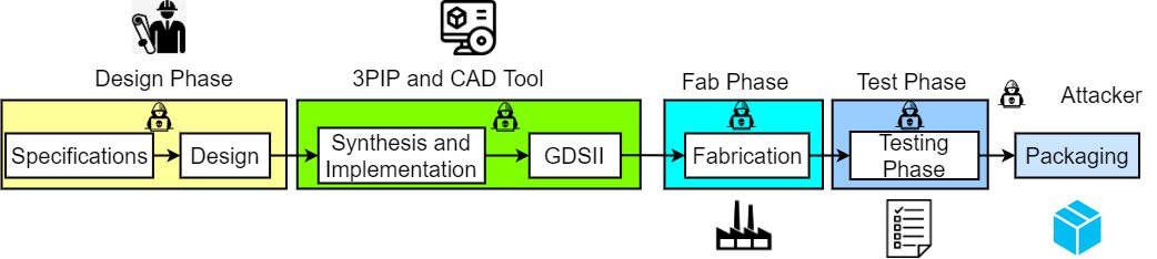
IC manufacturing with millions and billions of transistors has become the need of the hour to support large consumer market that constantly demands increasing performance and speed. The semiconductor industry has progressed a lot in terms of speed and performance to satiate the needs but at the cost of manufacturing the IC offshore as a majority of companies have gone fabless due to various economic, cost and technology reasons thus exposing the IC supply chain to adversaries/attackers causing trust issues. The base reason for fabricating the design offshore is the smaller technology node, lower the number better the speed, it offers. The IC fabrication goes through a variety of design processes and each stage has become an access point where attackers can get their hands on to serve malicious purposes. The IC manufacturing chain is highly complex and is susceptible to various threats both from the outside and inside. Figure 1 presents the supply chain process, each process block is vulnerable to different type of attacks [15]. This has impacted the fabrication business economy due to the threats that are posed by untrusted fabs like reverse engineering, hardware trojans and IP piracy [16, 17, 18]. The IC design house imports the IP - intellectual property - from the IP vendors which are then integrated with the custom designs in the design house. The finalized design is thus sent to the Fabrication vendors for manufacturing. The hardware level attack could be executed at any of these stages. Logic locking [19, 20, 21], aka obfuscation, is a defense mechanism that is used to hide the true functionality of the circuit to prevent design leakage even if the attacker gets the design netlist. Additional gates are embedded in various parts of the design to hide the functionality and these gates only act as transparent via media when correct logic is supplied. The correct logic is known as keys which are supplied to the circuit during the activation phase and are stored in the on-chip tamper proof memory. The activated IC works as designed only after the correct combination of the keys. The keys is a chain of ‘1’s and ‘0’s which is only known to the designer. With the state-of-the-art attacks [16, 17, 18] prevalent, protection using only obfuscation technique does not suffice to thwart the attack. A recent state-of-the-art attack known as SAT attack is based on the assumption that the attacker has access to the functional IC (IC activated by the designer using the correct key combinations) and the locked/obfuscated netlist has surged. The SAT attack [22] is based on the application of Distinguishing Input Patterns (DIPs) where the attack reduces key search space by iteratively applying DIPs to the obfuscated design and then applying the same DIPs to the functional IC thus eliminating incorrect key inputs. Along with logic locking type defense, split manufacturing [23] is a technique used to ‘split’ and manufacture different blocks of the design at different fabrication units. As a consequence, an IC responsible for activation of secondary IC could be manufactured at a trusted foundry, while other IC, at smaller technology, can be manufactured offshore (potential untrusted foundry). After manufacturing the designer stacks the two components together so the trusted platform can activate and control its untrusted counterpart. To achieve this methodology, an application to facilitate and evaluate different logic locking techniques against SAT attack was indispensable. The developed application will be described in the next chapter. Also, apart from the application, I was entrusted to develop and test hardware communication modules responsible for secure data transfer between the trusted and untrusted platforms. The same is presented in the next chapter.
1.1.2 Physical SCA
Data integrity and security became an essential part in the era of digital systems where privacy and confidentiality needs to be ensured. There have been a plethora of works addressing the attacks on systems, like those posed by malware [24, 25, 26, 9], reverse engineering of hardware [27, 28]; attacks on machine-learning assisted hardware-based malware detectors (HMDs) [29, 30, 31], adversarial attacks on machine learning [32], machine learning based attacks on hardware [33, 34], cache based side-channel attacks [35, 36, 37], etc. Of these, side-channel attack and cryptosystem has been discussed in this work. Cyrptographic mechanisms are employed to offer security to the data by encrypting the data streams with a secret key and transform the data into a human non-readable format. The attempt to exercise a brute force to decrypt the information is exhaustive and can even be unfeasible. To efficiently decode the secret key and decrypt the information, adversaries target utilizing the information obtained through side-channels, termed as side-channel attacks. Side-channels are inherent in any given design and side-channel attacks exploit the information from these rather than exploiting vulnerabilities in the software. There exist both physical and microarchitectural side-channels that can leak secure critical information through acoustics, electromagnetic (EM) radiations, power trace, thermal maps and cache-access information. Power signature based side-channel threats are a pivotal threat as power consumption is an inherent and preliminary characteristic of any digital system.
In this work I consider a power signature based side-channel attack on encryption algorithm executing on FPGAs as they are proliferating into data centers for compute-intensive operations such as encryption. For the power analysis based SCA to be successful, the attacker measures the power traces from the system while triggering crypto operations on the system. This trace is then studied statistically to deduce the secret key. The fundamental principle underlying this attack is that different modules (operations) of AES consume different power, and thereby studying the power trace reveals the operation, based on which the secret key can be deduced.
Pengyuan Yu et al. in [38] propose an intelligent place-and-route technique to facilitate symmetrical routing as a defense against power analysis SCA on FPGA. Work in [39] describes how a circuit can be transformed to a larger circuit to defend against probe-based physical SCAs, but, the technique proposed is very complex. Work in [40] and [41] describes algorithmic countermeasures to thwart SCAs which attempts to minimize the correlation between the intermediate values and the secret key ;and by algorithmically adding noise respectively. Also, circuit-level countermeasures are presented in papers [42, 43, 44, 45, 46]. It is observed that the existing defenses require modifications in physical designs, leading to larger overheads and design complexity.
To overcome these challenges and defend against power analysis SCA, I propose Power Swapper. More details about the proposed Power Swapper will be discussed in the coming chapters.
2 IC Reverse Engineering Defense
2.1 Trusted-Untrusted Design Integration
As discussed in the introduction section, a design could be subjected to IC reverse engineering (RE) attacks and design integrity attacks. Also, for security critical applications, the end design should be trustworthy. To address the IC manufacturing supply chain attacks [15, 16, 17, 18], the idea of the project is to integrate two chips post manufacturing - one chip being a trusted chip and other could be manufactured at an offshore untrusted environment. The trusted environment could be a secure facility/foundry, and the untrusted could be a manufacturing unit outside the secure zone. To protect the untrusted design (UD) from attacks, the design would be obfuscated before the tapeout phase. The obfuscation [47, 48, 49, 19, 20, 21] adds additional gates to the design that do not contribute to the end functionality, yet inserted to increase robustness against SAT-Solver or SAT attacks [22]. The design is executed in different phases and evaluating robustness against attacks is one of the most important parts. Usually, obfuscation of the design is achieved by running various algorithms on a system, which is a laborious effort. Moreover, after the design framework is handed over to the end user, the user may not be familiar with the technicalities of the aforementioned obfuscation defenses and attacks. Automating the frontend tasks was proposed as a panacea to reduce the efforts in evaluating the attack and to render the system end-user friendly. Next, we will discuss more on the automation tool.
2.2 Automation Tool for Design Security
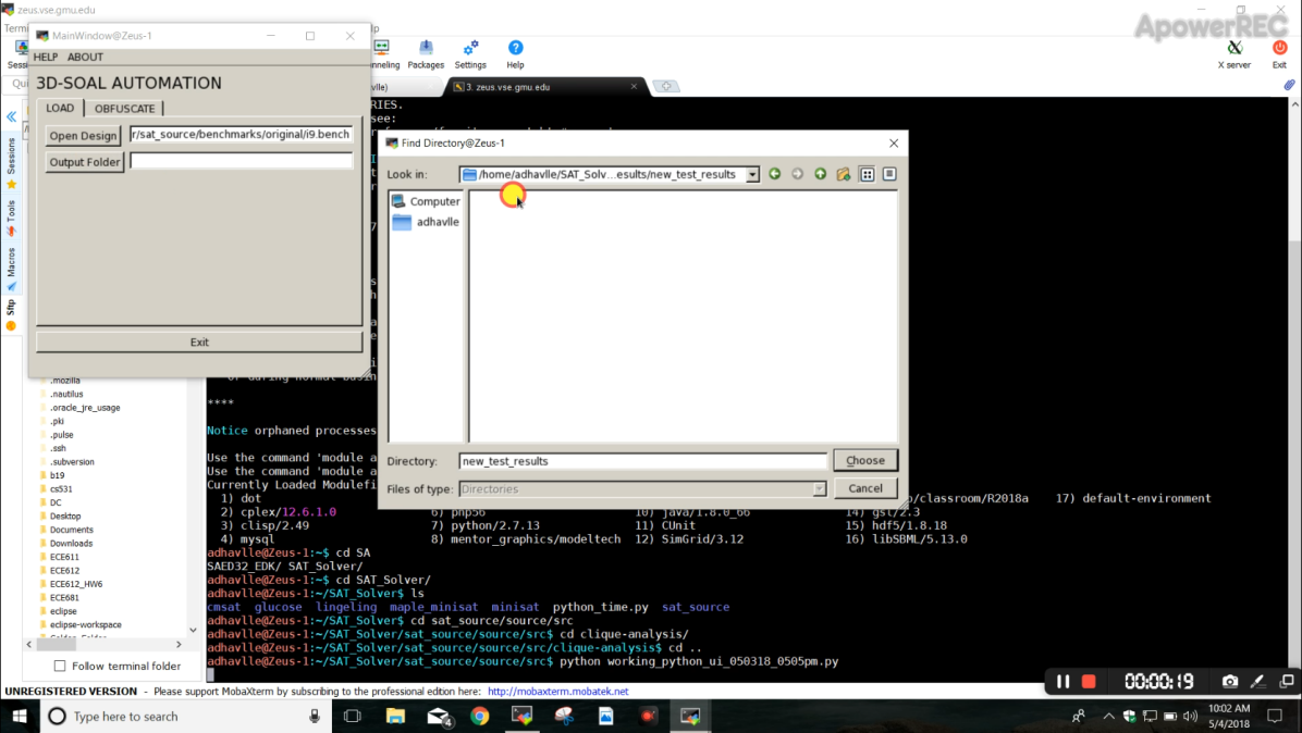
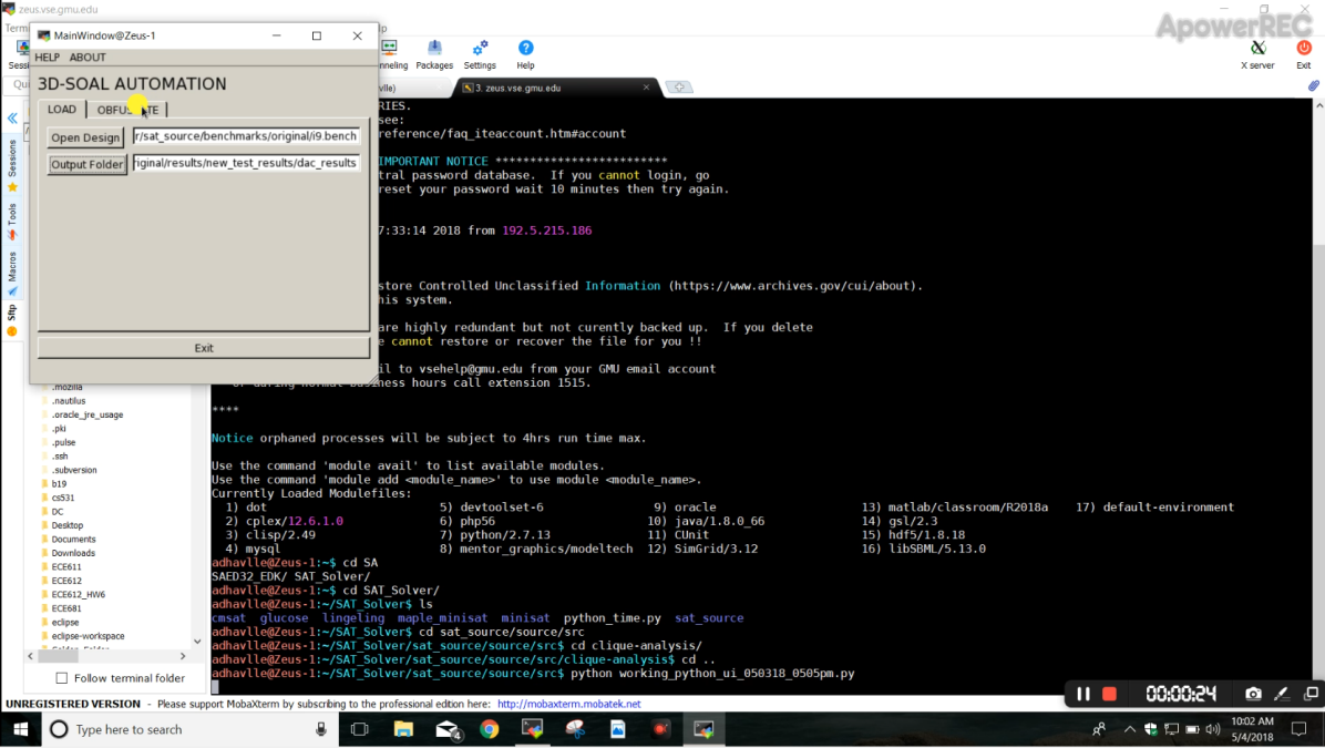
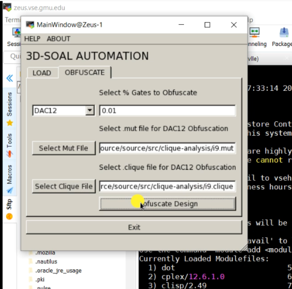
The automation application as shown in Figure 2 provides a user-friendly interface to obfuscate a design using various algorithms, and to de-obfuscate the same. Please note that the obfuscation algorithms are standard and I have no contributions towards them. My task was to build the application that could utilize the standard algorithms in the background.
The parameters the application is capable of selecting are listed below:
-
1.
The obfuscation algorithms the application can use are:
-
•
Iolts
-
•
Random
-
•
DAC12
-
•
TOC13MUX
-
•
TOC13XOR
-
•
-
2.
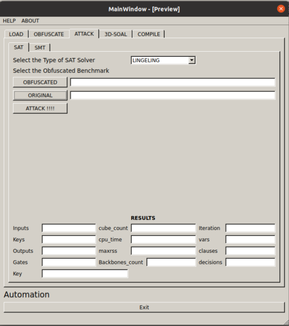
The Attack tab has SAT and SMT type solvers. Within SAT, the application allows for five different solvers.
-
•
Lingeling
-
•
CMSAT
-
•
Glucose
-
•
Maple_minisat
-
•
Minisat
-
•
-
3.
Number (in percent) of logic gates to obfuscate.
-
4.
Selecting specific files required for DAC12 algorithm - .MUT and .CLIQUE files.
-
5.
Select the input and output folders to choose a base design from and to store the resultant outputs.
Prerequisites to executing the application are:
-
1.
Ensure SAT solvers are installed on the system, which includes the dependencies also.
-
2.
Ensure Python is installed.
-
3.
Install Qt designer - this is a GUI designing application that takes less efforts than directly writing the Python code for the GUI blocks.
-
4.
Install PyQt-4/5 - this is an API to support the GUI designing.
- 5.
The steps to produce the obfuscated design is as follows:
-
1.
Use the Load tab in the application and select the base design to obfuscate. Refer to Figure 2.
-
2.
Select the output folder to store the resultant obfuscated design. Refer to Figure 3.
-
3.
Move to the Obfuscate tab of the application and choose the obfuscation algorithm, percent of gates to obfuscate, and selecting .MUT and .CLIQUE files, if DAC12 was chosen earlier. Refer to Figure 4.
-
4.
Hit the ‘obfuscate design’ button to start the task.
-
5.
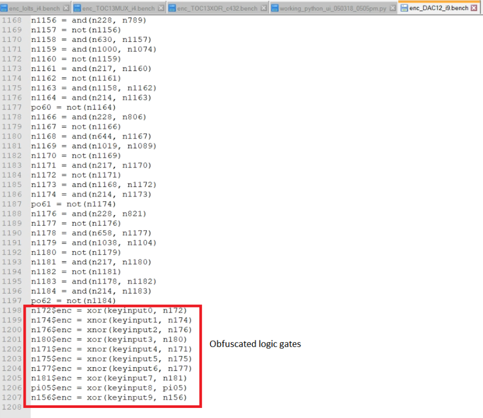
Find the generated file in the output folder chosen earlier, and verify the change in the resultant design file. Refer to Figure 5.
-
6.
For executing SAT-type attacks, click on the Attacks tab; select the type of solver, select an obfuscated design and original (unobfuscated) file; click the attack button to start the process. The results section shows different parameters of the outcome of the attack. These parameters are parsed by the script and shown in each of the boxes. Refer to Figure 6.
2.2.1 PyQt Code for Recreating a Basic Layout
2.2.2 User Interface (UI) designed in QT Designer
2.3 Reconfigurable Modules for Trusted-Untrusted Platform Communication
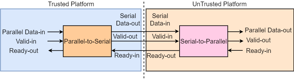
The trusted and untrusted platforms are stacked/connected together so the master platform can control the other untrusted platform. Depending on the scenario and other design constraints there may arise a need to either establish a serial (less wires and slower data) communication versus a parallel (more wires and faster data) communication, or vice versa. To address this, I was asked to design and test a parallel-to-parallel hardware communication modules. The interface of both the platforms is a serial connection, the final ends being a parallel data-in and data-out approach. The two platforms may have different operating clock speeds. This could also be referred as a clock domain crossing scenario. Hence, it is necessary to realize the design using finite state machine (FSM) approach. The block diagram of the communication blocks is shown in Figure 7; the block diagrams of the state machine is shown in Figure 8. Referring to Figure 7, the modules use a AXI interface to communicate with each other and other blocks of the higher level design. The AXI interface has standardized signal names to denote their functionality. The data bus could be an input or a output that takes data into the block or out from the block. The valid signal denotes that the content on the data bus is ‘valid’ and ready to be consumed. The valid could be an input or an output signal depending on whether it is placed on the consumer side or the generator side. A consumer block accepts the data from the block previous to it; a generator block generates some data and feeds it to the consumer block after it. A ready signal indicates the block is ready to process next piece of data.
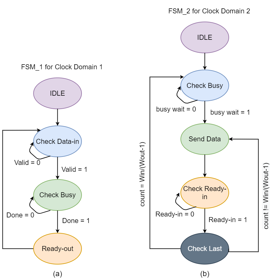
The two state machines with different clocks is shown in Figure 8. The state machine begins in Idle state; part (a) waits for the valid signal and content on the data bus. The Check Busy state checks if the done signal goes high, after which the ready-out signal is set to ‘1’. The done signal is active when the data is processed by the block and ready to be transferred to the next block. In part (b), the Check Busy state expects a busy wait signal based on which it moves to the next state, Send Data, which converts the parallel data into serial data. While this conversion occurs, the state machine checks for the last piece of data to be processed in the Check Last state. After the conversion of data, the Send Data block will transfer the data out on the bus if the Ready-in signal is active.
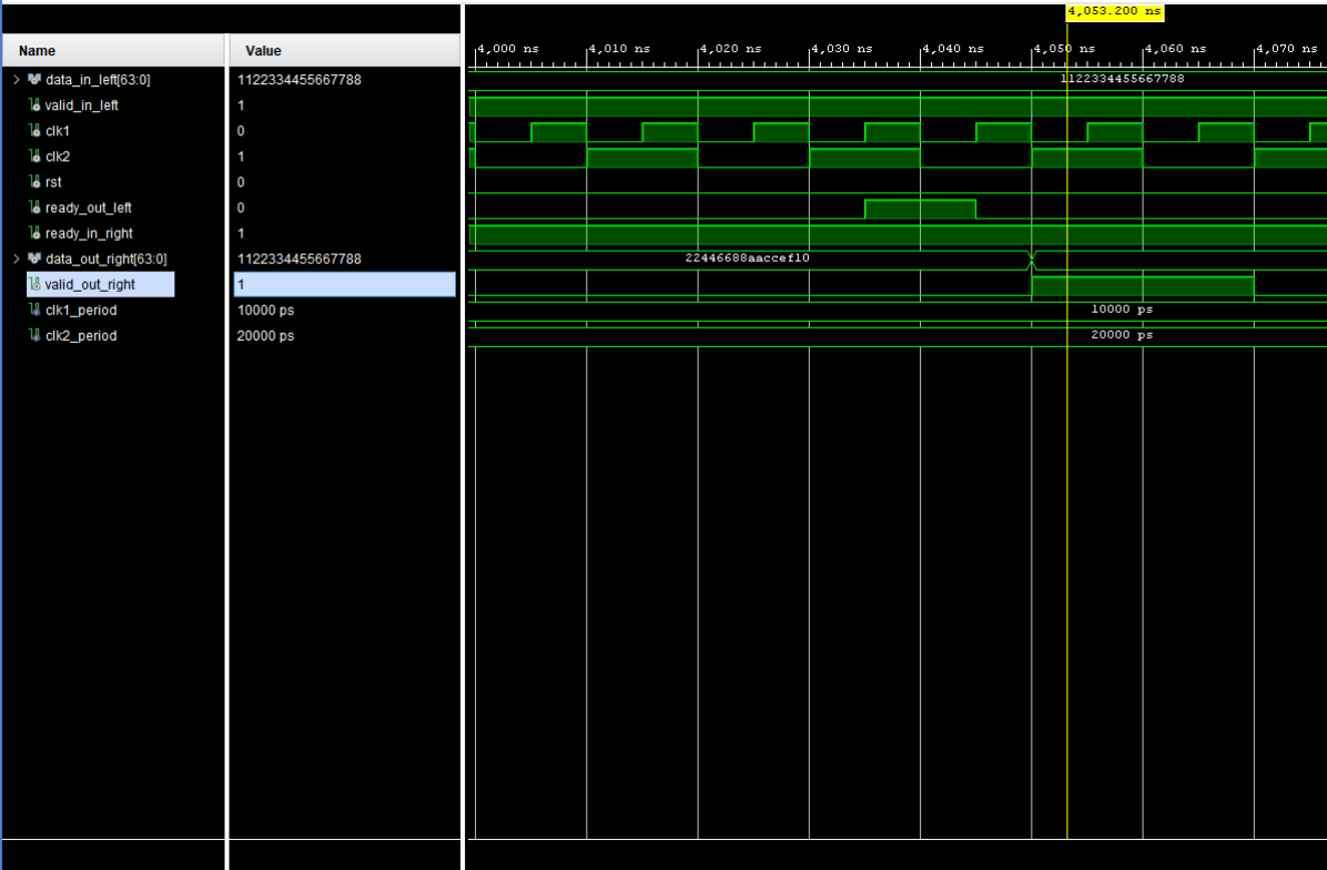
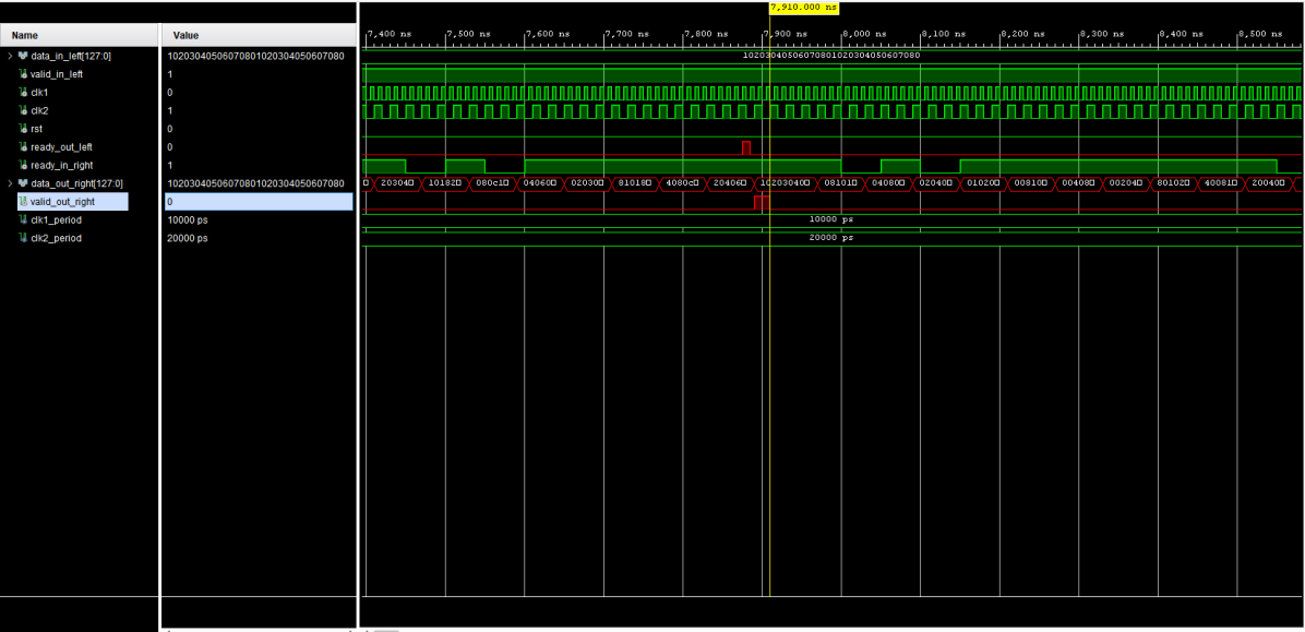
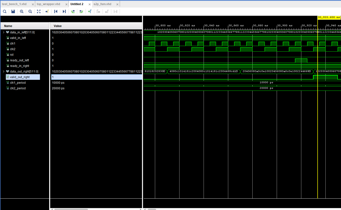
The modules were realized in VHDL language and Xilinx Vivado was used to simulate, synthesize and generate waveforms. The simulation waveforms for 64, 128, and 512 bit data input are shown in Figure 9, 10, and 11. It can be seen in the diagrams that the ready-out signal is set to ‘1’ when the data processing is complete. The code for the parallel to serial hardware module is presented in Listing 3. The resource utilization for 64, 128 and 512-bits configuration implemented on a Zedboard FPGA is shown in Figure 1, 2, and 3.
2.3.1 VHDL code for Parallel to Serial Module
| Total Resource | Slice LUTs | Slice Registers | F7 Muxes | F8 Muxes | Bonded IOB | BUFCTRL |
|---|---|---|---|---|---|---|
| 53200 | 106400 | 26600 | 13300 | 200 | 32 | |
| Top Wrapper Utilization (%) | 0.10 | 0.09 | 0.03 | 0.03 | 67.50 | 6.25 |
| P2S Utilization (%) | 0.07 | 0.02 | 0.03 | 0.03 | 0.0 | 0.0 |
| S2P Utilization (%) | 0.03 | 0.08 | 0.0 | 0.0 | 0.0 | 0.0 |
| Total Resource | Slice LUTs | Slice Registers | F7 Muxes | F8 Muxes |
|---|---|---|---|---|
| 53200 | 106400 | 26600 | 13300 | |
| Top Wrapper Utilization (%) | 0.15 | 0.16 | 0.06 | 0.06 |
| P2S Utilization (%) | 0.11 | 0.02 | 0.06 | 0.06 |
| S2P Utilization (%) | 0.04 | 0.14 | 0.0 | 0.0 |
| Total Resource | Slice LUTs | Slice Registers | F7 Muxes | F8 Muxes | Bonded IOB | BUFCTRL |
|---|---|---|---|---|---|---|
| 53200 | 106400 | 26600 | 13300 | 200 | 32 | |
| Top Wrapper Utilization (%) | 0.35 | 0.52 | 0.26 | 0.24 | 515.50 | 6.25 |
| P2S Utilization (%) | 0.30 | 0.02 | 0.26 | 0.24 | 0.0 | 0.0 |
| S2P Utilization (%) | 0.04 | 0.50 | 0.0 | 0.0 | 0.0 | 0.0 |
3 Defense Against CPA-based Physical Side-Channel Attack
3.1 Physical Side-Channel Attack
In this section, an introduction to physical side-channel attacks is provided, followed by the setup used for power measurement and a background of correlation power analysis (CPA). Data integrity and security became an essential part in the era of digital systems where privacy and confidentiality needs to be ensured. There have been a plethora of works addressing the attacks on systems, like those posed by malware [24, 25, 26, 9], reverse engineering of hardware [27, 28], attacks on machine-learning assisted hardware-based malware detectors (HMDs) [29, 30], adversarial attacks on machine learning [32], cache based side-channel attacks [35, 50, 37], etc. Of these, side-channel attack on cryptosystem is discussed in this work. To prevent such attacks, cyrptographic mechanisms are employed to offer security to the data by encrypting the data streams with a secret key and transform the data into a human non-readable format. The attempt to exercise a brute force to decrypt the information is exhaustive and can even be unfeasible. To efficiently decode the secret key and decrypt the information, adversaries target utilizing the information obtained through side-channels, termed as side-channel attacks. Side-channels are inherent in any given design and physical side-channel attacks exploit the information from these rather than exploiting vulnerabilities in the software. There exist both physical and microarchitectural side-channels that can leak secure critical information through acoustics, electromagnetic (EM) radiations, power trace, thermal maps and cache-access information [51, 52, 53, 54, 55]. Power signature based side-channel threats are a pivotal threat as power consumption is an inherent and preliminary characteristic of any digital system.
This work considers a power signature based side-channel attack on encryption algorithm executing on FPGAs as they are proliferating into data centers for compute-intensive operations such as encryption. For the power analysis based SCA to be successful, the attacker measures the power traces from the system while triggering crypto operations on the system. This trace is then studied statistically to deduce the secret key. The fundamental principle underlying this attack is that different modules (operations) of AES consume different power, and thereby studying the power trace reveals the operation, based on which the secret key can be deduced.
Pengyuan Yu et al. in [38] propose an intelligent place-and-route technique to facilitate symmetrical routing as a defense against power analysis SCA on FPGA. Work in [39] describes how a circuit can be transformed to a larger circuit to defend against probe-based physical SCAs, but, the technique proposed is very complex. Work in [40] and [41] describes algorithmic countermeasures to thwart SCAs which attempts to minimize the correlation between the intermediate values and the secret key ;and by algorithmically adding noise respectively. Also, circuit-level countermeasures are presented in papers [42, 43, 44, 45, 46]. It is observed that the existing defenses require modifications in physical designs, leading to larger overheads and design complexity.
To overcome these challenges and defend against power analysis SCA, I propose Power Swapper. More details on the proposed Power Swapper are presented below.
3.1.1 Introduction to Correlation Power Analysis
The setup harnessed for measuring the power is described in this section followed by a brief introduction to the process of CPA (Correlation Power Analysis) analysis for key extraction.
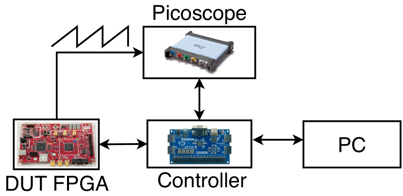
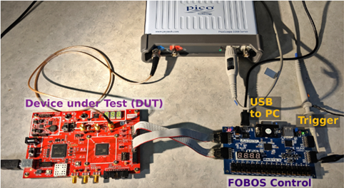
FOBOS Setup The setup is built specially for measuring FPGA core power for physical side-channel attack analysis. The setup is termed as FOBOS (Flexible Open-source workBench fOr Side-channel analysis) [56, 57]. Figure 12 shows the block diagram of the FOBOS setup, Figure 13 is a photo of the components connected together for power measurement. The Controller is an Artix-7 based FPGA that receives the test vectors from the PC and communicates with the DUT FPGA (Device Under Test) which is the target FPGA platform running the AES implemenatation. The target initiates instances of the AES cryptosystem and delivers the results to the controller. Meanwhile, the controller also triggers Picoscope measurement cycle at the same time as the AES and delivers the measured power and the cipher text to the PC. The Picoscope captures the entire trace of the AES cycle and keeps iterating for every new AES cycle. The PC runs the Python scripts that are responsible for sending the test vectors and key (secret key) to the controller and accumulating all the results in a numpy array. The FOBOS is completely reconfigurable to suit the specific needs of the measurements and application. The setup is described in more detail in [56, 57].
Attack Model The attack model and the assumptions for a successful attack have been described below:
-
1.
Physical access: The adversary needs to have physical access to the cryptosystem for obvious reasons - the CPA analysis needs power traces as one of its inputs to calculate key bytes. The physical access taps the power input to the FPGA so the traces can be captured.
-
2.
Access to PT: The attacker also has access to the plaintext(PT) which is used by the system.
-
3.
Access to the AES implementation: The adversary needs to have an idea of how the AES has been implemented internally. This is needed to choose the appropriate attack point and decide whether only PT and power traces are sufficient to succeed the attack phase.
-
4.
AES timing: It is helpful for the attacker to have access to the time it takes for the intermediate values to be processed and be available at the output of the point of attack. This has been discussed in the next section.
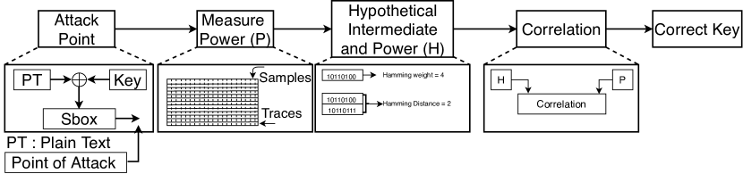
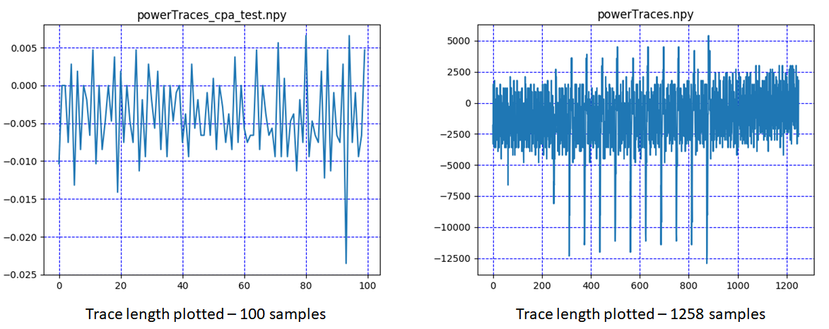
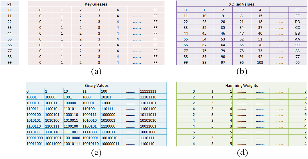
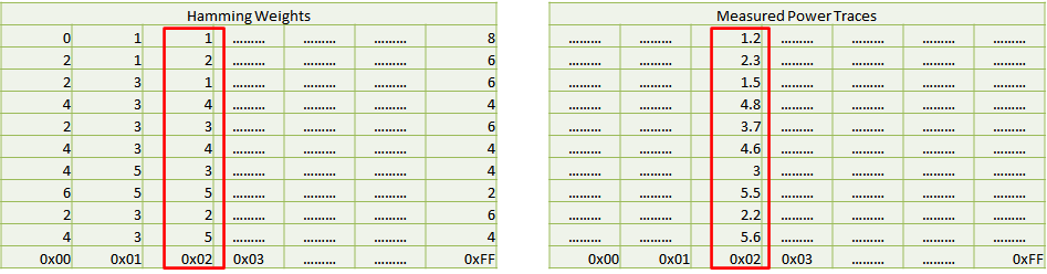
CPA Analysis Figure 14 illustrates the process of how CPA analysis is performed on the system to derive the correct combination of key input. In design, the length of the plain text, cipher text and the key is 128 bits wide. The adversary must try to derive as much correct key bits as possible to break the cryptosystem security. Once the correct key has been derived, the adversary gets access to the systems where the same key was used for providing security. There are some assumptions that are precursory to the tampering of the system which have been discussed previously. The CPA attack is one of the ways in which an adversary can gain access to the AES key. Referring to Figure 14, the attacker begins by deciding the point of attack. The point of attack is selected such that the value (output) available relates to the combination of the plaintext and the key (the attacker does not have access to the key, partial or whole). The block in conventional AES implementation that is chosen is the ‘sbox’ aka substitution box. The contents of this lookup table is open sourced and hence even the attacker has access to it. As discussed previously, the attacker has access to the time it takes for the data to reach the point of attack or the sbox in this case. Proceeding further, the power to the DUT FPGA is measured and stored. Power values corresponding to one full AES cycle are known as samples, whereas, the individual runs of the AES (with different test vector, with the same key) are known as traces; sample traces with different sample sizes is shown in Figure 15. The CPA then involves calculating the hypothetical intermediate and the hypothetical power, shown in Figure 16. The output of a sbox block is tried to mimic here to calculate the hypothetical power. Thing to note here is the attacker has no access to the actual key used and hence, it tries to generate all possible values (typically it is done byte wise, so a total of 256 possible values). After the output value of the sbox is known, by a combination of guessed key and plaintext, hamming weight or distance is calculated to represent power. This hypothetical power and the actual measured power are then correlated to see which power output value (hypothetical) corresponds strongly with the actual measured value and the correct key is the one that corresponds to that hypothetical value calculated previously; the process of correlation is shown in Figure 17. By iterating through this process a number of times the full key is derived.
4 Power-Swapper: Proposed Defense Against CPA-based Side-Channel Attack
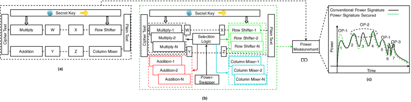
The proposed Power Swapper has been outlined in Figure 18 where part (a) shows the internal structure of a conventional FPGA cryptosystem where each module has its own power consumption rating. The attacker then performs the power analysis on the system and then through statistical methods the adversary tries to deduce the secret key information. This is possible due to the fact that the instantaneous power consumption value would correspond to the operation of module. Based on these sequence of operations, the attacker can deduce the secret information. As shown in Figure 18(c), the power consumption waveform has seven peaks in total each corresponding to some operation. For instance, peak 1 and 5 have the same magnitude and inferred to belong to the same operation ‘OP-1’; peaks 2, 3 and 4 belong to ‘OP-2’ and so on. The information leakage in this case is maximum and it is highly correlating the power traces which can lead to leakage of secret information.
On the contrary, Figure 18(b) shows the cyrptosystem being secured by Power Swapper where the internally implemented functional modules still perform the same tasks as in a conventional FPGA shown previously except for the fact that there are other approximate-blocks that perform the same function but are designed in such a way that they have different power consumption ratings. These approximate blocks are chosen randomly during runtime by the selection logic which is controlled by the Power Swapper. Since each block still does the same task, there will not be any deviations in the functionality of the application.
Power-Swapper uses physically unclonable function (PUF) block within the Power Swapper to make the selection process random and unpredictable to the attacker. Figure 18(c) shows the waveform of the power traces corresponding to the proposed Power Swapper where some of the peaks show different values compared to the conventional FPGA power trace. Peak 1 which previously would give information of operation OP-1 now corresponds to OP-2 as per the attacker based on the power analysis.
Peak 3, which belonged to OP-2 now corresponds to the power consumption similar to OP-1. As can be seen, the victim is not altered yet the power traces are completely different and they are not known to and which mislead the attacker. Even if the attacker tries to study a large number of patterns to find the power trace modifications injected by the approximate modules, the efforts would become futile as the trace will keep sweeping between different power magnitudes due to the randomness derived from the PUF block. The power consumption magnitudes of the alternate implementations of basic blocks range from p1 to p5 where p1 < p2< p3< p4< p5 and the range of the alternate block-1 performing the operations is in the range p1 to p3, while that of the block-2 would be in range of p2 to p4 while yet another block would have it in p3 to p5 range. As there is overlap in the power consumption range, one approximate block’s power corresponds to some other block’s range when they both are swapped during runtime. Hence, the attacker would be forced to deduce the sequence of operations as two different ones whereas internally the same row shifting operation was performed with two different power signatures.
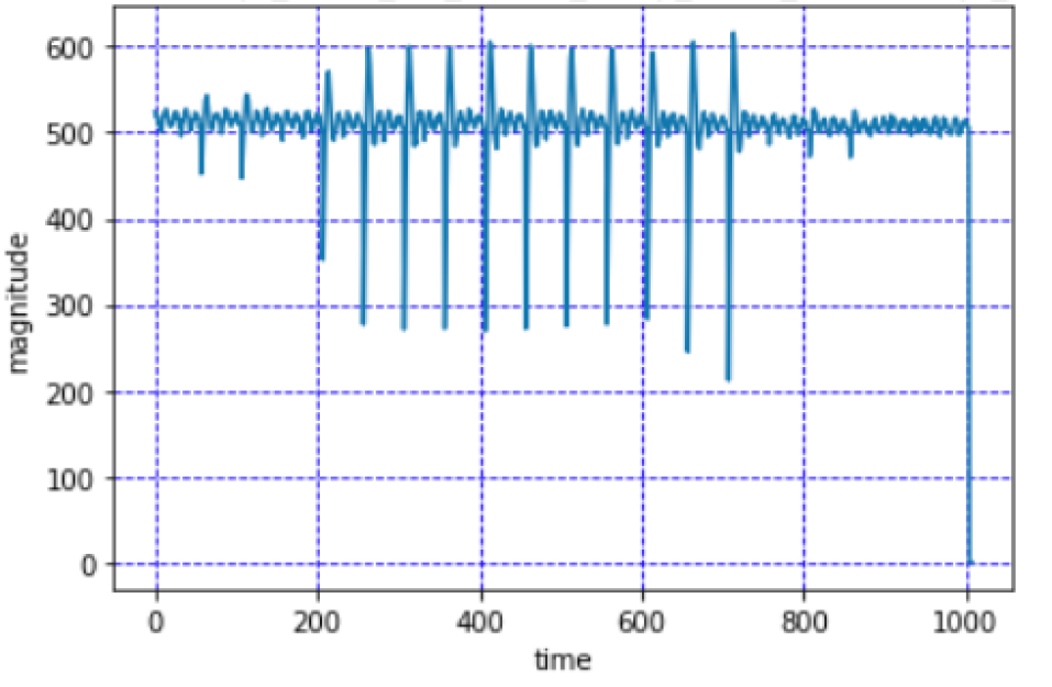
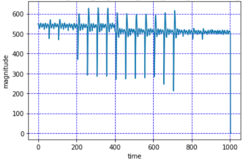
Refer to Figure 19 which shows the power trace of AES implementation without the proposed method. The trace was observed with the following parameters: DUT clock as 1 MHz, sampling frequency of 50 MHz and ADC sampling rate of 50MSps. If we observe the magnitude of the waveform and compare that with the magnitude shown in Figure 20, the change can be vividly seen owing to the approximate modules that perform essentially the same task but with a different power consumption. The way this disrupts the CPA power analysis is: the hypothetical intermediate that will be calculated by the adversary will remain the same (as discussed previously); key and the plaintext remain the same for a particular AES cycle. On the contrary, the actual power consumption would come out to be different and hence, if not for all the parts of the key but for some, parts of the key the adversary derives is incorrect disrupting the CPA analysis. Figure 20 illustrates an increase in the magnitude but it can also be the opposite depending how the approximate modules are designed. Hence, theoretically, if one harnesses the approximate modules for enhancing security in FPGA based crypto implementations, power analysis based side channel attacks could be thwarted.
4.0.1 Experimental Results
The experimental setup used for capturing AES traces (without Power Swapper) was: 1. Artix-7 based FPGA controller, CW305 Artix FPGA Target DUT board, PicoScope 5000 series for capturing the power traces, system clock frequency used was 1 MHz. The cyrpto application implemented on the DUT board was AES [56] with 128 bits of plaintext, key and output cipher text. Pearson correlation was used to calculate hypothetical power. Automation scripts were used to provide test vectors to the DUT and 1 million traces were collected for analysis.
Refer to Table 4 for the power traces observed by the attacker with Power Swapper. As can be seen from table, the information deduced by the attacker based on power consumption values are completely different compared to the actual operation executed on the core. The modified power signatures observed by the attacker are highlighted in red. The modified signatures are a result of the Power Swapper choosing one of the approximate blocks. Similarly, referring to Table 5, the key derived using CPA without and with Power Swapper has been shown. The bytes/nibble that were wrongly correlated to the key guesses - as described previously - have been highlighted. These wrong portions of the keys are observed as the effect of the approximate modules introduced by Power Swapper . It is to be noted that the length of the plaintext and key does not in anyway affect the efficacy of the proposed method. The results in the Tables 4, 5 provide sufficient proof that by employing approximate modules, cryptosystems can be rendered resilient against power analysis based side-channel attacks.
Ovehead Analysis: As with every system, the proposed methodology will also have overheads. The Power Swapper requires that approximate modules be added to the original implementation of AES and these modules will be selected during the application execution. Needless to say, the modules will require additional space on the FPGA fabric along with some increase in power consumption. Switching between these modules will also lead to small overheads. The small, if not insignificant, overhead would be the trade off between security and power/area. The resource utilization for two variants of AES is shown in Table 6 and 7. One variant is implemented as a base version, without any pragmas in Vivado HLS 2019; Table 6 presents the resource utilization results. Another variant is implemented using pipeline and loop unroll pragmas; the results are presented in Table 7. Both variants essentially function the same except that the power signatures are different. The total hardware resource utilization will be decided based on how many variants of AES, or blocks within AES, is utilized to include a range of power signatures for each block. The results presented in Table 6 and 7 are for reference only; they will scale based on the security to area/power tradeoff chosen as per the required resiliency against attack.
| Scenario | Victim Power Trace | Power Trace with Power Swapper | |
|---|---|---|---|
| Instance-1 | Instance-2 | ||
| Scenario-1 | OP-1/OP-2/OP-3/OP-4 | OP-3/OP-2/OP-1/OP-4 | OP-2/OP-3/OP-4/OP-1 |
| Scenario-2 | OP-1/OP-1/OP-4/OP-3 | OP-2/OP-3/OP-2/OP-1 | OP-3/OP-1/OP-1/OP-3 |
| Trace # | Correct key | Incorrect key with Power Swapper |
|---|---|---|
| Trace-1 | 51720187c36e0c8523acb8535a870703 | 51522187ca6ea28523acb8e35a870793 |
| Trace-2 | d14a900c7391d64101fe33a85b0793cb | a14a90dc7391d63201fe33a85b1693cb |
| Name | BRAM 18K | DSP48E | FF | LUT | URAM |
| DSP | - | - | - | - | - |
| Expression | - | - | 0 | 64 | - |
| FIFO | - | - | - | - | - |
| Instance | 0 | - | 1245 | 6648 | - |
| Memory | - | - | - | - | - |
| Multiplexer | - | - | - | 183 | - |
| Register | 0 | - | 1311 | 32 | - |
| Total | 0 | 0 | 2556 | 6895 | 0 |
| Available | 280 | 220 | 106400 | 53200 | 0 |
| Utilization (%) | 0 | 0 | 2 | 12 | 0 |
| Name | BRAM 18K | DSP48E | FF | LUT | URAM |
| DSP | - | - | - | - | - |
| Expression | - | - | 0 | 1478 | - |
| FIFO | - | - | - | - | - |
| Instance | 0 | - | 4356 | 16698 | - |
| Memory | - | - | - | - | - |
| Multiplexer | - | - | - | 162 | - |
| Register | 0 | - | 3717 | 32 | - |
| Total | 0 | 0 | 8073 | 18370 | 0 |
| Available | 280 | 220 | 106400 | 53200 | 0 |
| Utilization (%) | 0 | 0 | 7 | 34 | 0 |
4.0.2 Conclusion and Future Work
In this work, I discussed the physical power SCAs, discussed the severity of the threats posed and delineated the works in the past. In contrast to the existing works, proposed Power Swapper will preserve the victim’s secret information without any modifications to the victim algorithm in itself. I hope the community will be intrigued by the preliminary results discussed in this work and I plan to develop this work in future to deliver more details of the mechanism that would benefit the security critical processes.
Acknowledgement
I would like to thank Dr.Jens-Peter Kaps and Dr. Abubakr Abdulgadir from Cryptographic Engineering Research Group - George Mason University for providing access to the FOBOS [56] setup for power-side channel analysis, and offering all the kind help in configuring FOBOS for the experiments.
5 Conclusion
This thesis discussed the importance of security to computing systems. We discussed the attacks, like reverse engineering, threatening the security community and their capabilities to disrupt design confidentiality. Further, defense against IC reverse engineering attacks was discussed which includes the automation application for logic locking defense and robustness evaluation against attacks, followed by the design of hardware communication modules. Further, physical side-channel attack on crypto systems on FPGA was discussed in detail along with a proposed defense against such attack. The thesis also includes full working code for the automation application and hardware module.
References
- [1] S. Bavikadi, A. Dhavlle, A. Ganguly, A. Haridass, H. Hendy, C. Merkel, V. J. Reddi, P. R. Sutradhar, A. Joseph, and S. M. P. Dinakarrao, “A Survey on Machine Learning Accelerators and Evolutionary Hardware Platforms,” IEEE Design & Test, pp. 1–1, 2022.
- [2] S. Kasarapu, R. Hassan, H. Homayoun, and S. M. Pudukotai Dinakarrao, “Scalable and demography-agnostic confinement strategies for covid-19 pandemic with game theory and graph algorithms,” COVID, vol. 2, no. 6, pp. 767–792, 2022.
- [3] S. Kasarapu, S. Shukla, R. Hassan, A. Sasan, H. Homayoun, and S. M. PD, “Cad-fsl: Code-aware data generation based few-shot learning for efficient malware detection,” 2022.
- [4] S. Kasarapu, R. Hassan, S. Rafatirad, H. Homayoun, and S. M. P. Dinakarrao, “Demography-aware covid-19 confinement with game theory,” in 2021 IEEE 3rd International Conference on Artificial Intelligence Circuits and Systems (AICAS), 2021, pp. 1–4.
- [5] S. Shukla, G. Kolhe, S. M. PD, and S. Rafatirad, “Rnn-based classifier to detect stealthy malware using localized features and complex symbolic sequence,” in 2019 18th IEEE International Conference On Machine Learning And Applications (ICMLA), 2019, pp. 406–409.
- [6] S. Shukla, G. Kolhe, S. M. P D, and S. Rafatirad, “Stealthy malware detection using rnn-based automated localized feature extraction and classifier,” in 2019 IEEE 31st International Conference on Tools with Artificial Intelligence (ICTAI), 2019, pp. 590–597.
- [7] S. Shukla, G. Kolhe, S. M. P. D, and S. Rafatirad, “Microarchitectural events and image processing-based hybrid approach for robust malware detection: Work-in-progress,” in Proceedings of the International Conference on Compliers, Architectures and Synthesis for Embedded Systems Companion, 2019.
- [8] S. Shukla, P. D. Sai Manoj, G. Kolhe, and S. Rafatirad, “On-device malware detection using performance-aware and robust collaborative learning,” in Design Automation Conference (DAC), 2021, pp. 967–972.
- [9] A. Dhavlle, S. Shukla, S. Rafatirad, H. Homayoun, and S. M. Pudukotai Dinakarrao, “Hmd-hardener: Adversarially robust and efficient hardware-assisted runtime malware detection,” in Design, Automation Test in Europe Conference Exhibition (DATE), 2021, pp. 1769–1774.
- [10] S. Barve, S. Shukla, S. M. P. Dinakarrao, and R. Jha, “Adversarial attack mitigation approaches using rram-neuromorphic architectures,” in Proceedings of the 2021 on Great Lakes Symposium on VLSI, 2021, p. 201–206.
- [11] S. Shukla, G. Kolhe, P. Sai Manoj, and S. Rafatirad, “Work-in-progress: Microarchitectural events and image processing-based hybrid approach for robust malware detection,” in 2019 International Conference on Compliers, Architectures and Synthesis for Embedded Systems (CASES), 2019, pp. 1–2.
- [12] S. Kasarapu, S. Shukla, R. Hassan, A. Sasan, H. Homayoun, and S. M. PD, “Cad-fsl: Code-aware data generation based few-shot learning for efficient malware detection,” in Proceedings of the Great Lakes Symposium on VLSI 2022, 2022, p. 507–512.
- [13] S. Shukla, G. Kolhe, H. Homayoun, S. Rafatirad, and S. M. P D, “Rafel - robust and data-aware federated learning-inspired malware detection in internet-of-things (iot) networks,” in Proceedings of the Great Lakes Symposium on VLSI 2022, 2022, p. 153–157.
- [14] A. Dhavlle and S. Shukla, “A novel malware detection mechanism based on features extracted from converted malware binary images,” 2021. [Online]. Available: https://arxiv.org/abs/2104.06652
- [15] A. Dhavlle, R. Hassan, M. Mittapalli, and S. M. P. Dinakarrao, “Design of hardware trojans and its impact on cps systems: A comprehensive survey,” in 2021 IEEE International Symposium on Circuits and Systems (ISCAS), 2021, pp. 1–5.
- [16] M. Rostami, F. Koushanfar, and R. Karri, “A primer on hardware security: Models, methods, and metrics,” Proceedings of the IEEE, vol. 102, no. 8, pp. 1283–1295, Aug 2014.
- [17] R. Torrance and D. James, “The state-of-the-art in semiconductor reverse engineering,” in Proceedings of the 48th Design Automation Conference, ser. DAC ’11. New York, NY, USA: ACM, 2011, pp. 333–338. [Online]. Available: http://doi.acm.org/10.1145/2024724.2024805
- [18] M. M. Tehranipoor, U. Guin, and S. Bhunia, “Invasion of the hardware snatchers,” IEEE Spectr., vol. 54, no. 5, pp. 36–41, May 2017. [Online]. Available: https://doi.org/10.1109/MSPEC.2017.7906898
- [19] J. A. Roy, F. Koushanfar, and I. L. Markov, “Epic: Ending piracy of integrated circuits,” in Proceedings of the Conference on Design, Automation and Test in Europe, ser. DATE ’08. New York, NY, USA: ACM, 2008, pp. 1069–1074. [Online]. Available: http://doi.acm.org/10.1145/1403375.1403631
- [20] J. Rajendran, H. Zhang, C. Zhang, G. S. Rose, Y. Pino, O. Sinanoglu, and R. Karri, “Fault analysis-based logic encryption,” IEEE Transactions on Computers, vol. 64, no. 2, pp. 410–424, Feb 2015.
- [21] Y. Xie and A. Srivastava, “Anti-sat: Mitigating sat attack on logic locking,” IEEE Transactions on Computer-Aided Design of Integrated Circuits and Systems, vol. 38, no. 2, pp. 199–207, Feb 2019.
- [22] P. Subramanyan, S. Ray, and S. Malik, “Evaluating the security of logic encryption algorithms,” in 2015 IEEE International Symposium on Hardware Oriented Security and Trust (HOST), May 2015, pp. 137–143.
- [23] F. Imeson, A. Emtenan, S. Garg, and M. Tripunitara, “Securing computer hardware using 3d integrated circuit (IC) technology and split manufacturing for obfuscation,” in Presented as part of the 22nd USENIX Security Symposium (USENIX Security 13). Washington, D.C.: USENIX, 2013, pp. 495–510. [Online]. Available: https://www.usenix.org/conference/usenixsecurity13/technical-sessions/presentation/imeson
- [24] S. Shukla, G. Kolhe, S. M. P D, and S. Rafatirad, “Stealthy malware detection using rnn-based automated localized feature extraction and classifier,” in International Conference on Tools with Artificial Intelligence (ICTAI), 2019.
- [25] S. Shukla, G. Kolhe, S. M. PD, and S. Rafatirad, “Rnn-based classifier to detect stealthy malware using localized features and complex symbolic sequence,” in International Conference On Machine Learning And Applications (ICMLA), 2019.
- [26] S. Shukla, G. Kolhe, S. M. P. Dinakarrao, and S. Rafatirad, “On-device Malware Detection using Performance-aware and Robust Collaborative Learning,” Design Automation Conference (DAC), 2021.
- [27] G. Kolhe and et.al., “Security and complexity analysis of lut-based obfuscation: From blueprint to reality,” in Int. Conference On Computer Aided Design, 2019.
- [28] Z. Chen, G. Kolhe, and et.al, “Estimating the circuit deobfuscating runtime based on graph deep learning,” in Design, Automation and Test in Europe Conference (DATE), 2020.
- [29] S. M. P. Dinakarrao, S. Amberkar, S. Bhat, A. Dhavlle, H. Sayadi, A. Sasan, H. Homayoun, and S. Rafatirad, “Adversarial attack on microarchitectural events based malware detectors,” in Design Automation Conference, 2019.
- [30] S. Shukla, G. Kolhe, S. M. P. D, and S. Rafatirad, “Microarchitectural events and image processing-based hybrid approach for robust malware detection: Work-in-progress,” in Proceedings of the International Conference on Compliers, Architectures and Synthesis for Embedded Systems Companion, 2019.
- [31] A. Dhavlle and S. Shukla, “A novel malware detection mechanism based on features extracted from converted malware binary images,” 2021.
- [32] S. Barve, S. Shukla, S. M. P. Dinakarrao, and R. Jha, “Adversarial Attack Mitigation Approaches using RRAM Neuromorphic Architectures,” GLSVLSI, 2021.
- [33] M. Meraj Ahmed, A. Dhavlle, N. Mansoor, P. Sutradhar, S. M. Pudukotai Dinakarrao, K. Basu, and A. Ganguly, “Defense against on-chip trojans enabling traffic analysis attacks,” in 2020 Asian Hardware Oriented Security and Trust Symposium (AsianHOST), 2020, pp. 1–6.
- [34] M. M. Ahmed, A. Dhavlle, N. Mansoor, S. M. P. Dinakarrao, K. Basu, and A. Ganguly, “What can a remote access hardware trojan do to a network-on-chip?” in International Symposium on Circuits and Systems (ISCAS), 2021, pp. 1–5.
- [35] F. Brasser, L. Davi, A. Dhavlle, and et al., “Advances and throwbacks in hardware-assisted security: Special session,” in Conference on Compilers, Architecture and Synthesis for Embedded Systems, 2018.
- [36] A. Dhavlle, S. Rafatirad, K. Khasawneh, H. Homayoun, and S. M. P. Dinakarrao, “Imitating functional operations for mitigating side-channel leakage,” IEEE Transactions on Computer-Aided Design of Integrated Circuits and Systems, vol. 41, no. 4, pp. 868–881, 2022.
- [37] A. Dhavlle, R. Mehta, S. Rafatirad, H. Homayoun, and S. M. P. D, “Entropy-shield:side-channel entropy maximization for timing-based side-channel attacks,” in 21 st International Symposium on Quality Electronic Design (ISQED), 2020.
- [38] P. Yu and P. Schaumont, “Secure fpga circuits using controlled placement and routing,” in IEEE/ACM International Conference on Hardware/Software Codesign and System Synthesis, 2007.
- [39] Y. Ishai, A. Sahai, and D. Wagner, “Private circuits: Securing hardware against probing attacks,” in Advances in Cryptology, 2003.
- [40] P. C. Kocher, J. Jaffe, and B. Jun, “Differential power analysis,” in Proceedings of the 19th Annual International Cryptology Conference on Advances in Cryptology, ser. CRYPTO ’99, 1999.
- [41] S. Chari, C. S. Jutla, J. R. Rao, and P. Rohatgi, “Towards sound approaches to counteract power-analysis attacks,” in Advances in Cryptology — CRYPTO’ 99, M. Wiener, Ed., 1999.
- [42] D. Suzuki, M. Saeki, and T. Ichikawa, “Random switching logic: A new countermeasure against dpa and second-order dpa at the logic level,” IEICE Transactions, vol. 90-A, pp. 160–168, 01 2007.
- [43] E. Trichina, “Combinational logic design for aes subbyte transformation on masked data,” IACR report, Tech. Rep., 2003.
- [44] Shengqi Yang, W. Wolf, N. Vijaykrishnan, D. N. Serpanos, and Yuan Xie, “Power attack resistant cryptosystem design: a dynamic voltage and frequency switching approach,” in Design, Automation and Test in Europe, 2005.
- [45] A. Dubey, R. Cammarota, and A. Aysu, “Maskednet: The first hardware inference engine aiming power side-channel protection,” in International Symposium on Hardware Oriented Security and Trust (HOST), 2020, pp. 197–208.
- [46] R. Matovu, A. Serwadda, A. V. Bilbao, and I. Griswold-Steiner, “Defensive charging: Mitigating power side-channel attacks on charging smartphones,” in Conference on Data and Application Security and Privacy. Association for Computing Machinery, 2020, p. 179–190.
- [47] J. Rajendran, M. Sam, O. Sinanoglu, and R. Karri, “Security analysis of integrated circuit camouflaging,” in Proceedings of the 2013 ACM SIGSAC Conference on Computer & Communications Security, ser. CCS ’13. New York, NY, USA: ACM, 2013, pp. 709–720. [Online]. Available: http://doi.acm.org/10.1145/2508859.2516656
- [48] A. Vijayakumar, V. C. Patil, D. E. Holcomb, C. Paar, and S. Kundu, “Physical design obfuscation of hardware: A comprehensive investigation of device and logic-level techniques,” Trans. Info. For. Sec., vol. 12, no. 1, pp. 64–77, Jan. 2017. [Online]. Available: https://doi.org/10.1109/TIFS.2016.2601067
- [49] M. Yasin, B. Mazumdar, O. Sinanoglu, and J. Rajendran, “Camoperturb: secure IC camouflaging for minterm protection,” in Proceedings of the 35th International Conference on Computer-Aided Design, ICCAD 2016, Austin, TX, USA, November 7-10, 2016, 2016, p. 29.
- [50] A. Dhavlle, S. Bhat, S. Rafatirad, H. Homayoun, and S. M. P. D, “Work-in-progress: Sequence-crafter: Side-channel entropy minimization to thwart timing-based side-channel attacks,” in Conference on Compliers, Architectures and Synthesis for Embedded Systems (CASES), 2019.
- [51] F.-X. Standaert, Introduction to Side-Channel Attacks, 2010.
- [52] F. Koeune and F.-X. Standaert, A Tutorial on Physical Security and Side-Channel Attacks, 2005.
- [53] C. Shepherd, K. Markantonakis, N. van Heijningen, D. Aboulkassimi, C. Gaine, T. Heckmann, and D. Naccache, “Physical fault injection and side-channel attacks on mobile devices: A comprehensive analysis,” Computers & Security, vol. 111, p. 102471, 2021.
- [54] M. A. Al Faruque, S. R. Chhetri, A. Canedo, and J. Wan, “Acoustic side-channel attacks on additive manufacturing systems,” in International Conference on Cyber-Physical Systems (ICCPS), 2016, pp. 1–10.
- [55] S. S. Mirzargar and M. Stojilović, “Physical side-channel attacks and covert communication on fpgas: A survey,” in International Conference on Field Programmable Logic and Applications (FPL), 2019, pp. 202–210.
- [56] A. Abdulgadir, W. Diehl, and J.-P. Kaps, “An open-source platform for evaluating side-channel countermeasures in hardware implementations of lightweight authenticated ciphers,” in International Conference on Reconfigurable Computing and FPGAs (ReConFig), Cancun, Mexico, Dec 2019.
- [57] R. Velegalati and J.-P. Kaps, “Towards a Flexible, Opensource BOard for Side-channel analysis (FOBOS),” Cryptographic architectures embedded in reconfigurable devices, CRYPTARCHI 2013, June 2013.