Inhale: Enabling High-Performance and Energy-Efficient In-SRAM Cryptographic Hash for IoT
Abstract.
In the age of big data, information security has become a major issue of debate, especially with the rise of the Internet of Things (IoT), where attackers can effortlessly obtain physical access to edge devices. The hash algorithm is the current foundation for data integrity and authentication. However, it is challenging to provide a high-performance, high-throughput, and energy-efficient solution on resource-constrained edge devices. In this paper, we propose Inhale, an in-SRAM architecture to effectively compute hash algorithms with innovative data alignment and efficient read/write strategies to implicitly execute data shift operations through the in-situ controller. We present two variations of Inhale: Inhale-Opt, which is optimized for latency, throughput, and area-overhead; and Inhale-Flex, which offers flexibility in repurposing a part of last-level caches for hash computation. We thoroughly evaluate our proposed architectures on both SRAM and ReRAM memories and compare them with the state-of-the-art in-memory and ASIC accelerators. Our performance evaluation confirms that Inhale can achieve 1.4 - 14.5 higher throughput-per-area and about two-orders-of-magnitude higher throughput-per-area-per-energy compared to the state-of-the-art solutions.
1. Introduction
Information security has long been an issue of significant concern and investment willingness. After entering the era of big data, hospitals, large corporations, and governments have exerted considerable effort to assure data security and integrity (Cawthra et al., 2020). The current algorithms behind data integrity and authentication are the hashing algorithms. For instance, the widely used Transport Layer Security protocol provides data integrity for identity authentication by utilizing the hash algorithm (Dierks and Rescorla, 2008). In addition, six of the seven candidate algorithms in the final round of the latest NIST post-quantum cryptography standardization process are based on hash algorithms (Alagic et al., 2020), five of which are specifically based on the Keccak secure hash algorithm (Dworkin, 2015) (the NIST winner for SHA-3), which accounts for almost 50% of the total algorithm’s cycles (Alagic et al., 2020; Avanzi et al., 2019). Keccak is also heavily used in cryptocurrencies, such as Ethereum (Wood, 2014), Monero (Möser et al., 2017), and NEM (Zhang et al., 2018a). Therefore, providing a high-throughput and energy-efficient solution for Keccak is critical for miners.
Moreover, an increasing number of edge devices are becoming capable of device-to-device, device-to-cloud, and device-to-user communication (Madakam et al., 2015). To prevent attackers from tampering with sensitive data, these interactions must be constructed on top of identity authentication, which is the ability of individual devices to determine each other’s identity through certain processes (Mahmoud et al., 2015). Numerous approaches have been presented to mitigate IoT security concerns (Won et al., 2018; Obiri et al., 2021; Singla and Bertino, 2018). Since all of these mechanisms rely on hash algorithms, there is an imminent need for a high-throughput, low-latency, and energy-efficient solutions for hash algorithms on resource-constrained edge devices.
Several hardware acceleration solutions are proposed to improve throughput, latency, or hardware overhead. Tillich et al. (Tillich et al., 2009) use small LUTs to store intermediate variables to reduce the latency. Akin et al. (Akin et al., 2010) exploit a pipelined design to implement different stages of hashing algorithms to improve the throughput. Moreover, Pessl et al. (Pessl and Hutter, 2013) propose to reduce on-chip storage overhead by interleaving input data. However, it is extremely challenging to optimize for high-throughput, low-latency, energy-efficiency, and area-efficiency all at the same time.
Recent studies based on in-memory (Bhattacharjee et al., 2017; Nagarajan et al., 2019; Zhang et al., 2018b; Reis et al., 2022; Zhang et al., 2022) computing are proposed to improve the performance and energy efficiency of secure-related algorithms, especially hash algorithms. Nagarajan et al. (Nagarajan et al., 2019) propose a ReRAM-based implementation of SHA-3, named SHINE. To optimize for latency, the authors present a pipeline design by replicating the memory arrays in each stage of the pipeline, thus, trading hardware overhead and throughput-per-unit-area for latency. Moreover, their design does not generalize to other hashing algorithms. In addition, it expands the trusted computing base (TCB) to the off-chip memory, which exposes more space to attackers. Zhang et al. (Zhang et al., 2018b) propose Recryptor, a reconfigurable cryptographic processor capable of accelerating finite field multiplication and reduction, AES, and Keccak using in-memory computing. However, due to the complex peripheral circuitry, Recryptor only runs at 28.8 MHz, which significantly limits the performance.
In this paper, we present Inhale, a high-performance, low-overhead, and energy-efficient hashing accelerator for low-end IoT devices by repurposing 6T SRAM subarrays and turning them into active large vector computation units. Inhale maximizes the inherent parallelism and bitline computational capability of memory subarrays to provide a high-throughput, low-latency, and energy-efficient solution for the SHA-3 algorithm with negligible area overhead (less than 2% compared to conventional SRAM arrays). The benefits of Inhale are enabled by three main reasons; (1) Based on our analysis, we find that 76% of the operations in SHA-3 are shift operations. Inhale reduces about 90% of shift operations by proposing an effective Lane Per Row (LPR) data alignment technique strategy to implicitly perform the shift operations using a memory-mapped controller. (2) We present an efficient in-place read/write strategy to perform the majority of the computation on the fly, thus, reducing the number of cycles and memory usage for intermediate data. (3) Inhale design reuses the same memory array and peripherals to implement all the stages of SHA-3, thus significantly saving area. The combination of these benefits makes Inhale yield significantly higher throughput-per-area-per-energy compared to the state-of-the-art.
Unlike prior work, our design does not expand the TCB to the off-chip components (similar to Intel SGX (Costan and Devadas, 2016) and AMD SME (Kaplan et al., 2016)). Though SHA-3 is discussed here as a case-study, Inhale is capable of computing other variants of the hash algorithm (e.g. SHA-1, SHA-2), block cipher algorithms (e.g. AES-256), as well as hash-based and finite-field-multiplication-based key establishment mechanisms and digital signature algorithms in the post-quantum era.
In summary, the paper makes the following contributions:
-
•
We present Inhale, an in-SRAM hashing engine with four-fold latency, throughput, area, and energy benefits for accelerating SHA-3 by exploiting compatible data alignment with minimal hardware modification. Inhale can be realized either by re-purposing existing last-level caches or as a separate on-chip crypto-engine. Our proposed architecture provides the effective use of memory capacity with an efficient read/write strategy and flexible support for varying message sizes in hash computation, which can accommodate a broad range of SRAM array sizes on a wide variety of IoT devices.
-
•
To reduce latency, we suggest a data alignment optimized for shift-intensive applications such as SHA-3. By implicitly performing inter-lane shift operations via the controller, a significant number of shift operations in the SHA-3 are replaced by in-situ control commands, which not only reduces latency but also, in conjunction with an efficient read/write strategy, effectively reduces the capacity overhead of intermediate variables.
-
•
We present two different variations of Inhale, Inhale-Flex and Inhale-Opt, and evaluate them on SRAM and ReRAM-based memory arrays. The results demonstrate that on the same memory technology, Inhale is able to achieve up to 172 throughput-per-area-per-energy compared to state-of-the-art in-memory implementations. To separate the architectural and technology contributions of Inhale and have an apples-to-apples comparison with prior work, we evaluate SHINE (Nagarajan et al., 2019) on SRAM (SHINE-SRAM) and find that our solution achieves 3.6 higher throughput-per-area than SHINE-SRAM due to architectural contribution and 3.4 better throughput-per-area due to the technology benefits.
2. Background and Threat Model
2.1. SHA-3 Algorithm
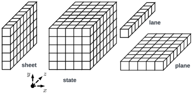
The construction and verification of digital signatures, key derivation, and the generation of pseudo-random bits are the primary functions of the hash algorithm, which is an essential component of the information security domain. SHA-3 is the third generation of standard hash functions, based on the implementation of the Keccak algorithm. The SHA-3 algorithm, unlike its predecessors, is a permutation-based cryptographic function. SHA-3 hashing heavily relies on the structure of the Keccak sponge function. The sponge structure is capable of data transformation, i.e., transforming arbitrary-length inputs into arbitrary-length outputs. The fundamental function in Keccak is a permutation selected from the set of seven Keccak- permutations, abbreviated Keccak-, where is the width of the permutation. In the sponge structure, the width of the permutation corresponds to the width of the State. The State is organized as a grid of five-by-five Lanes whose length is and . The naming conventions for parts of the Keccak- State used throughout the paper are shown in Fig. 1. In this paper, we discuss Keccak-f[1600] for SHA3-256. However, Inhale architecture can simply support all the Keccak permutations by adjusting the number of columns each Lane occupies in the array thanks to our lane-per-row data layout.
Keccak has five stages of computing () in one round. Let’s take one round of Keccak- as an example. Suppose we have a 1600-bit input State, which according to the naming conventions (Fig. 1), we can refer to as , where . The computations in five stages are as follows (Dworkin, 2015):
-
:
-
:
-
:
-
:
-
:
,
where the constant in the stage is the rotation offset depending on the location of the Lane, and in the stage is the round constant which is different for each of 24 rounds in Keccak-. For different , the number of rounds is equal to . The output of each round will be XORed with the next piece of the message (1088 bits in Keccak-) as the input of the next round of hashing (Dworkin, 2015) (see Fig. 5(c)).
2.2. Computing in SRAM
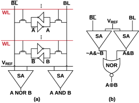
By activating more than one row in the SRAM subarray, in-SRAM processing can perform bitline computing (Jeloka et al., 2016). Fig. 2 represents the logical operations that 6T SRAM can support. Using several activated wordlines and sensing amplifiers (SAs), AND and NOR operations are directly implemented in SRAM, as shown in Fig. 2(a). The SA on the bitline () can only detect a voltage greater than if every cell in the activated rows connected to the contains the value ‘1’. This indicates that the SA will detect the value ‘1’, achieving element-wise AND operation. The SA on the bitline-bar () will sense a voltage higher than only if all the cells in the activated rows connected to the corresponding contain ‘1’, which, in turn, implies that all the cells in the activated rows connected to the corresponding contain ‘0’. Only if all the cells in the active rows connected to the corresponding bitline-bar () contain ‘1’ would the SA on the detect a voltage greater than , which suggests that all the cells in the activated rows connected to the corresponding bitline contain ‘0’. This indicates that the SA will detect the value ‘1’, achieving element-wise NOR operation. With the ability of logical bit-wise AND and NOR operations, the XOR operation can be achieved, as shown in Fig. 2(b).
Several studies based on SRAM computing are proposed (Aga et al., 2017; Eckert et al., 2018; Fujiki et al., 2019; Subramaniyan et al., 2017). Cache Automaton employs a sense-amplifier cycling mechanism to read out several bits in a single time slot, hence lowering input symbol match time by a large margin (Subramaniyan et al., 2017). Compute Cache increases the logical operations by slightly changing the SA design, based on the specified NOR, AND, and XOR operations in (Aga et al., 2017). In this paper, we employ the XOR capability described in (Aga et al., 2017).
2.3. Threat Model
Following the standard Trusted Execution Environment (TEE) threat model (Costan and Devadas, 2016), we assume that only the CPU itself is trusted and considered secure. The CPU contains no hardware backdoors. An attacker cannot directly or indirectly obtain access to the CPU’s data.
3. Related Work
Several hardware acceleration solutions are proposed to improve the throughput, latency, or hardware overhead of Keccak/SHA-3. Tillich et al. (Tillich et al., 2009) use small LUTs to store intermediate variables to reduce the latency. Akin et al. (Akin et al., 2010) and Wong et al. (Wong et al., 2018) exploit a pipelined design to implement different stages of hashing algorithms to improve the throughput. Pessl et al. (Pessl and Hutter, 2013) implement SHA-3 on RFID by interleaving two adjacent Lanes to generate a 128-bit word for computation in order to reduce the necessary on-chip memory space, and Ramanarayanan et al. (Ramanarayanan et al., 2010) fabricated a reconfigurable hashing accelerator for multi-mode SHA algorithms using unified SHA bit-slices and configurable compression circuits. However, none of them optimizes for high-throughput, low-latency, energy-efficiency, and area-efficiency all at the same time.
Moreover, recent in-memory solutions for SHA-3 implementation are proposed. Bhattacharjee et al. proposed an implementation of SHA-3 based on ReRAM (Bhattacharjee et al., 2017). Twenty-five Lanes are aligned as a grid of 5 by 5 Lanes, and the 5-input XOR is used to provide high parallelism in computation. Although the authors use techniques such as stage fusion to reduce computational overhead, their implementation of basic XOR requires 12 cycles, thus significantly increasing the overall computational latency. Nagarajan et al. present a novel ReRAM-based SHA-3 accelerated solution, named SHINE (Nagarajan et al., 2019). The authors construct multi-bit XOR, 64-bit and arbitrary bit shift operations based on ReRAM arrays and employ these cascaded arrays for pipeline processing to achieve a high throughput SHA-3 solution. To optimize for latency, the authors present a pipeline design by replicating the memory arrays in each stage of the pipeline, thus trading hardware overhead and throughput-per-unit-area for latency. Moreover, their design does not generalize to other hashing algorithms. In addition, it expands the trusted computing base (TCB) to the off-chip memory which exposes more space to attackers. Zhang et al. present Recryptor, a general-purpose processor with in-memory computing capabilities to handle a variety of cryptographic algorithms for IoT security (Zhang et al., 2018b). To implement inner-lane and inter-lane shifts for and stages, Recryptor requires a large bit width or a multi-stage shifter, which can result in a high hardware overhead. Moreover, due to the complex peripheral circuitry, Recryptor only runs at 28.8 MHz, which significantly limits the performance.
While it is possible to improve individual metrics, to efficiently enable secure edge computing on resource-constrained IoT devices, a four-fold optimization for latency, throughput, area, and energy efficiency is required. In Section 5, we compare the performance, area and energy consumption of Inhale with (Tillich et al., 2009; Pessl and Hutter, 2013; Akin et al., 2010; Wong et al., 2018; Nagarajan et al., 2019; Zhang et al., 2018b).
4. Implementation
4.1. Overview
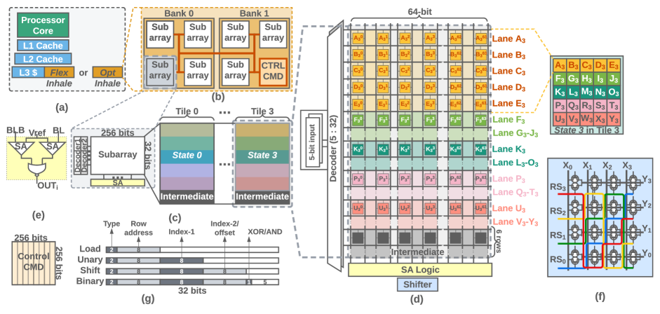
This section introduces Inhale, our proposed in-SRAM hashing architecture. Inhale can be realized either by re-purposing existing last-level caches in the device, named Inhale-Flex, or by developing a specialized on-chip SRAM-based acceleration engine, named Inhale-Opt, as depicted in Fig. 3 (a-b). Inhale-Opt trade flexibility for latency, throughput, area, and energy benefits by reducing the subarrays to size 32256. This reduces the subarray size and read/write latency, which enables higher frequencies and higher throughput.
Inhale’s smallest working unit requires two subarrays, one for data storage and computation and the other one for control and command data. Fig. 3(b) represents two banks, each with four subarrays, to illustrate our design. Based on the application requirements and power budget, banks can be utilized to hash up to independent messages in parallel, where is the number of subarrays in two adjacent banks, is the number of columns in each subarray, and is the width of a State (see Section 2.1). The rest of this section discusses data organization, implementation of each stage, the memory-mapped controller, and the generality of Inhale.
4.2. Data Organization
To efficiently utilize the limited SRAM capacity and to substantially reduce the number of shift cycles in and stages, the input and intermediate data of the SHA-3 algorithm are delicately placed in the same subarray, as shown in Fig. 3(c)-(d). The size of the subarray in Inhale-Opt design is 32256, which consists of 4 Tiles. Each Tile contains one State, i.e., the inputs of the SHA-3 algorithm. In each Tile, the first 25 rows are used to store twenty five 64-bit Lanes, as we call it lane-per-row data alignment. The rest of the rows are used for intermediate data. Since we use an in-place data read/write strategy, only 6 rows are enough to store intermediate data.
In Inhale-Flex design (which repurposes existing cache arrays), the size of the SRAM subarray is assumed to be 256256 following ARM Cortex-M0+ microcontroller (NXP, 2022). However, Inhale design can work with any subarray with a minimum of 32 rows (to store 25 Lanes and 6 intermediate data) and a minimum of 64 columns (to store a Lane of 64-bit). If the row number of the array exceeds 32, the extra rows can be utilized to store longer messages or more states in the Tile.
Prior work (Zhang et al., 2018b) arranges every 5 Lanes (320 bits) in one row and require 5 rows to store an entire State. Although this data alignment can highly expose the highest bit parallelism in stage, it incurs a significant number of shifts in , , and stages, where shift operations dominate. To reduce the shift cycles, they heavily rely on the high-overhead shifting modules, such as barrel shifter. Inhale utilizes lane-per-row data alignment, allowing all inter-lane shifts to be implicitly implemented by the controller simply by selecting the intended Lane instead of shifting.
In summary, our proposed lane-per-row data alignment has two advantages: 1) it significantly reduces the shift operations, which greatly reduces the need for large n-bit shifters. Almost every stage in the SHA-3 algorithm has inter-lane shifts. Specifically, , and requires inter-lane shifts to perform data alignment before XOR operations (e.g. C[(x-1)], C[(x+1)] in , A[(x+3y)] in , and A[(x+1)], A[(x+2)] in according to (Dworkin, 2015). Inhale implements these shift operations implicitly, thus, introducing area, latency, and energy benefits, and 2) it enables flexibility of mapping computation on smaller subarray sizes (i.e., only 32 rows and 64 columns are enough for Inhale to work), which are most efficient on resource-constrained edge devices. This is unlike prior work that requires the number of columns to be at least 320. Although we are discussing the data alignment for Keccak- in this paper (the largest setting), our data alignment can also accommodate other settings of Keccak by simply adjusting the number of bits per Lane.
4.3. Implementation of SHA-3 Stages
Theta () Stage: Theta () stage includes a series of XOR, inter-lane shift, and intra-lane shift operations on the original State of 1600 bits. In general, all Lanes within the same Sheet (Fig. 1) need to perform bit-wise XOR operations to obtain an additional intermediate Plane. Then, each Lane is bit-wise XORed with its corresponding Lane in the intermediate Plane to obtain the final Plane. At the last step, each Lane is bit-wise XORed with the corresponding Lane in the final Plane. The bit-wise XOR operation here is achieved by using two decoders to activate two rows simultaneously. We follow the bitline XOR functionality implementation in (Aga et al., 2017), which costs 3 times longer than a single subarray read/write access.
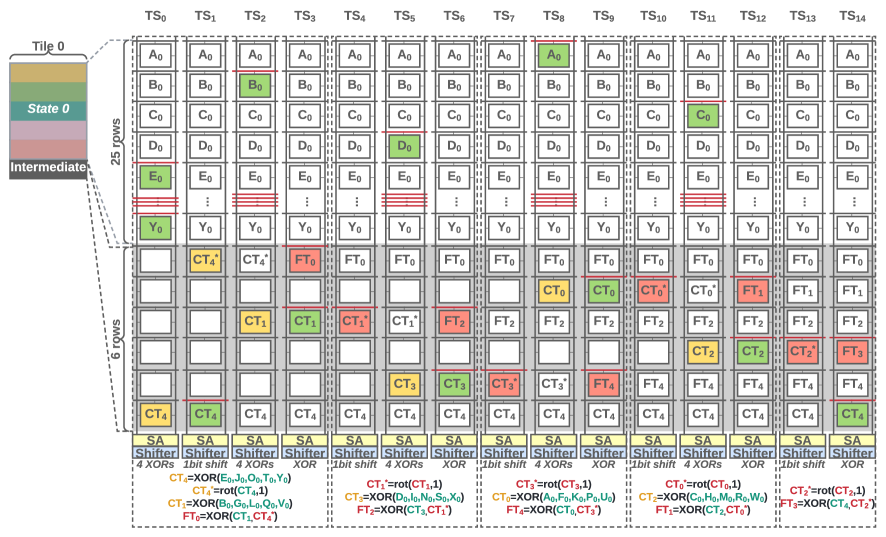
Fig. 4 demonstrates how the in-place read/write strategy is implemented in several time steps (TS) and explains why only 6 intermediate rows are enough for 1 round of computation. The first 25 rows store the 25 Lanes, and the next 6 rows store the intermediate data. In the first 4 time steps (), 4 XORs for , one 1-bit shift, 4 XORs for , and a single XOR are done. In particular, in , the first in-place operation is performed. The generated by , is activated with the line where is located, and then, the XOR operation is performed. The result is written back to , i.e., in-place computing. All the cells with the in-place operations are marked in red. In , 8 time steps utilize the in-place operations. Thus, we are able to save 40% space for the intermediate rows. This, in turn, results in the fewer number of required rows in Inhale design, and effectively translates to shorter read/write latency.
After we generate the five Lanes in the intermediate rows (), we need to XOR the different Lanes located in the same Sheet with the corresponding Lane in the intermediate rows. For example, needs to be respectively XORed with , , , , and , and overwrite the Lanes in the State with the obtained results. The complete correspondences are , , , , . Theta stage takes a total of 210 cycles, comprising 50 XOR operations and 5 inner-lane 1-bit shift operations for 25 Lanes.
Rho () and Pi () Stage: For the Rho stage, all the Lanes need to be inner-lane shifted with a certain number of bits according to their positions in the State. For example, the at needs to be shifted 62 bits to the right. Due to the randomness characteristic of the shift in the Rho stage, we use a 64-bit barrel shifter to perform these irregular shifts. For the Pi stage, since we use the lane-per-row data organization, the inter-lane shift in the Pi stage can be implicitly implemented by the memory-mapped controller. Specifically, no physical operation is done in the Pi stage. However, the controller selects the intended row (i.e., Lane) later in the Chi stage to get the correct data. Rho stage incurs a total of 50 cycles for 25 inner-lane shift operations, whereas the Pi stage is implicitly completed by an in-situ controller at no cost.
Chi () and Iota () Stage: In the Chi stage, each Lane needs to perform a series of operations with the next two Lanes that are on the same Plane. Since all its operations depend only on the data in the same Plane, we can use the in-place read/write strategy (similar to the Theta stage) to perform operations Plane-by-Plane to save intermediate rows. Specifically, to generate the results of the five Lanes (e.g., ) in the first Plane after the Chi stage, we first use bitline computing to perform NOT operations on each of the five Lanes, and write the results of NOTs () into the five intermediate rows. Then we perform AND operations between these Lanes and corresponding original Lanes (e.g., ) and write the results back to the corresponding row in the intermediate row. Finally, the original Lanes, which have not been overwritten from the beginning, are now XORed with the corresponding Lane in the intermediate rows, and the results of XORs are written back to the original position instead of the intermediate rows. Since we only compute the next Plane after finishing the computation of the previous Plane, only 5 intermediate rows are required.
In the Iota stage, we only need to bit-wise XOR the first Lane with pre-computed 64-bit data (). Since the data contains only 64 bits, we can use the control signal consisting of the data for data transfer without storing twenty-five 64-bit data in the subarray in advance. By placing this data in different Tiles, we can implement the XOR operation in the Iota stage in parallel. When three consecutive Lanes require three XORs and two implicit inter-lane shift operations, the Chi stage’s 75 XOR operations require a total of 300 cycles. Iota is a trivial stage, requiring only four cycles for one XOR and a write-back in one round.
4.4. Control Implementation
The control of the inhale is implemented by an inter-bank controller and a control subarray storing pre-generated control signals. As depicted in Fig. 3(b), the inter-bank controller is responsible for retrieving control signals from the control subarray and broadcasting them to the target subarrays during the corresponding clock cycles. The pre-generated control commands are stored in the control subarray in the format depicted in Fig. 3(g). The first two bits (i.e., [0:1]) specify one of the four commands: LOAD command for loading Round Constants (RCs), UNARY command for NOT operation, SHIFT command for shift operation, and BINARY command for XOR and AND operation. For subarrays with different numbers of rows, the row indexes are represented with different bit widths. In 256256 subarrays, [2:9] provides the row index of the command’s result. The LOAD instruction contains the row index of the row to be written. Then, the 64-bit RC is created and delivered to the target subarrays. After receiving the RC, the target subarray will write them to the intermediate rows of different Tiles in order to perform the computation. [10:17] in the UNARY command represents the row index of its operand. BINARY and SHIFT have two operands. Therefore, bits in the location of [18:25] specify the row index of the second operand (or the shift offset). The 26-th bit of BINARY command indicates, by a value of 0 or 1, whether the operation is XOR or AND. Longer control commands can be employed to handle larger subarrays. The memory-mapped controller broadcasts control signals to all arrays in the two adjacent banks, and the timely arrival of the control signals can be ensured by the pre-fetching techniques.
| Tech. | Max (MHz) | Area (KGE) | Latency (cycles) | Latency (ns) | Tput. (Mbps) | Tput./Area (Mbps/KGE) | Energy (nJ) | Tput./Area/En. (Mbps/(KGEnJ)) | |
| Inhale-Opt-SRAM | 28nm | 6.7K | 63.6 | 564 | 83.6 | 52K | 818 | 0.456 | 1.8K |
| Inhale-Flex-SRAM | 28nm | 6.1K | 386 | 564 | 91.9 | 47.3K | 123 | 0.596 | 206 |
| SHINE-1-SRAM | 28nm | 6.7K | 494 | 264 | 39.1 | 111K | 225 | - | - |
| SHINE-2-SRAM | 28nm | 6.7K | 717 | 140 | 20.7 | 210K | 293 | - | - |
| Recryptor(Zhang et al., 2018b) | 40nm | 28.8 | 600 | 139 | 4.8K | 226 | 0.377 | 2.03 | 0.186 |
| Inhale-Opt-ReRAM | 28nm | 2.4K | 19.1 | 564 | 235 | 18.6K | 970 | 0.348 | 2.79K |
| Inhale-Flex-ReRAM | 28nm | 2.3K | 56.3 | 564 | 240 | 18.1K | 322 | 0.446 | 721 |
| SHINE-1-ReRAM(Nagarajan et al., 2019) | 65nm | 2K | 494 | 264 | 132 | 33K | 66.8 | 4.13 | 16.2 |
| SHINE-2-ReRAM(Nagarajan et al., 2019) | 65nm | 2K | 717 | 140 | 70 | 62.2K | 86.7 | 3.5 | 24.8 |
| SHINE-1-ReRAM (projected) | 28nm | 4.6K | 494 | 264 | 56.9 | 76.5K | 155 | - | - |
| SHINE-2-ReRAM (projected) | 28nm | 4.6K | 717 | 140 | 30.2 | 144K | 201 | - | - |
| Akın(Akin et al., 2010) | 90nm | 455 | 10.5K | 25 | 54.9 | 19.8K | 1.89 | >43.5 | 0.043 |
| Tillich(Tillich et al., 2009) | 180nm | 488 | 56.3K | 25 | 51.2 | 21.2K | 0.377 | >43.5 | 0.009 |
| Pessl-V1 (Pessl and Hutter, 2013) | 130nm | 1 | 5.5K | 10.7K | 10.7M | 0.102 | 18.5e-6 | >43.5 | 4.25E-7 |
| Pessl-V2 (Pessl and Hutter, 2013) | 130nm | 1 | 5.9K | 7.4K | 7.4M | 0.147 | 24.9e-6 | >43.5 | 5.73E-7 |
| Wong(Wong et al., 2018) | 65nm | 1K | 105K | - | - | 48K | 0.457 | >43.5 | 0.011 |
* Energy of SHINE variants could not be simulated due to a lack of specifications, represented by ”-” in the Table.
SHINE-1 (optimized for area and power efficiency) and SHINE-2 (optimized for throughput and latency) are two variants of ReRAM-based SHA-3 accelerator presented in (Nagarajan et al., 2019).
4.5. Generality of Inhale Architecture
With lane-per-row data alignment, Inhale can accommodate messages of varying lengths (i.e., M bit, where M can be smaller or larger than 1088). In SHA-3, the hash value of a message with fewer than 1088 bits can be generated from 25 Lanes. For a message longer than 1088 bits, Lanes are required to calculate its hash value. For example, in Fig. 5(a), the last Tile has four independent messages (Msg0, …, Msg3). Assume that Msg0 has 2168 bits. Using Keccak as an example, Msg0 is split into two pieces, each of which consists of 1088 bits (i.e., requires seventeen 64-bit Lanes). Including the 8 Lanes shared by the two components, Msg0 should occupy a total of 42 rows. Unlike prior work that uses plane-per-row data alignment (i.e., storing the data of one Plane in a row), which cannot reuse the shared 8 Lanes, Inhale reuses the shared Lanes without modifying the data alignment or incurring any additional computational expense, hence reducing latency and capacity overhead.
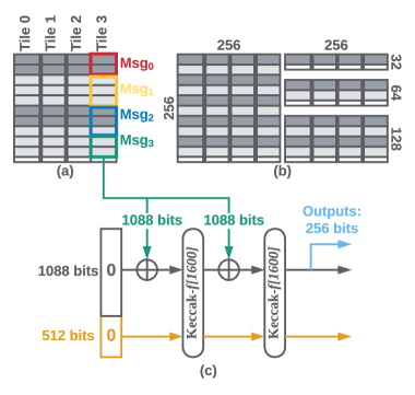
Inhale can also support subarrays of different sizes. As shown in Fig. 5(b), a 256256 subarray can be used to hold four Tiles, each of which can compute up to ten independent messages. Alternatively, we can use a 32256 subarray to store four independent messages to enable parallel processing. Inhale’s extensive support for variable subarray sizes enables its deployments on diverse IoT devices with varying SRAM array sizes. Note that the performance of different subarray sizes depends on read/write latency. In the evaluation section, we evaluate and compare the performance and overhead of the common 256256 subarray size (i.e., Inhale-Flex) and the smallest subarray size of 32256 (i.e., Inhale-Opt).
5. Evaluation
5.1. Evaluation Methodology
In this section, we evaluate the latency, area, throughput, energy, throughput-per-area-per-energy, and performance scaling of Inhale-Flex and Inhale-Opt, and compare them to prior in-memory solutions (Zhang et al., 2018b; Nagarajan et al., 2019) and other ASIC implementations (Pessl and Hutter, 2013; Wong et al., 2018; Tillich et al., 2009; Akin et al., 2010), as shown in Table 1. We use DESTINY simulator for area and energy simulation (Poremba et al., 2015). To decouple architectural contribution from the technology contribution and have an apples-to-apples comparison between SHINE and Inhale, we evaluate Inhale in 28nm ReRAM and SRAM, and also evaluate SHINE in 28nm SRAM and ReRAM. To decouple the area overhead from the technology node, we normalize the area overhead to the number of Kilo Gate Equivalent (KGE) (i.e., the area of a single NAND gate in the corresponding technology node).
The read and write access latency of 6T SRAM subarrays are extracted from the Synopsys Design Compiler with 45nm process and then projected to 28nm process. PyMTL3 (Jiang et al., 2020) and OpenRAM (Guthaus et al., 2016) are used to generate SRAM subarrays. The read and write latency of the ReRAM array are calculated from DESTINY simulator. The latency number in Table 1 represents the time consumed by one round of SHA-3 for each of the designs.
5.2. Latency Comparison
While Inhale-Flex design is based on 256-row memory arrays, Inhale-Opt design utilizes 32-row memory arrays, thus, having lower latency (10% reduction in conservative conditions). This is mainly because shorter subarrays have shorter bitlines, which results in lower read/write latency and higher frequency. Moreover, Inhale-Opt-SRAM and Inhale-Flex-SRAM designs achieve 58 and 52 better performance compared to Recryptor (Zhang et al., 2018b), respectively. This is because Recryptor is constrained by its complicated peripheral hardware (two-stage shifter and many MUXs) and can only operate at 28.8 MHz, resulting in a considerable performance limitation.
The SHINE-SRAM in 28nm technology has 53%-75% lower latency compared to the Inhale-SRAM design in the same technology node. This is mainly because SHINE uses a dedicated 5-bit XOR and 3-bit XOR logic that can compute 5-bit XOR or 3-bit XOR in four clock cycles. However, Inhale compute 5-bit XOR by performing in-SRAM XOR functionality for 2 bits at a time, each taking 3 clock cycles (i.e., ((( ) ) ) ), thus, a 5-bit XOR taking 12 cycles, a 3-bit XOR taking 6 cycles, and a 2-bit XOR requires three clock cycles. In summary, SHINE design trade the area-overhead to achieve 53%-75% lower latency compare to Inhale. However, the Inhale-SRAM design incurs 7.7 - 11.2 lower area-overhead compared to the SHINE-SRAM in the same technology node by sacrificing only 53%-75% latency. As a result, Inhale-Opt-SRAM can achieve 2.8 - 3.6 higher throughput per unit area than the SHINE-SRAM design, and Inhale-ReRAM can achieve 4.8 - 6.3 higher throughput-per-unit-area than the SHINE-ReRAM design! In addition, SHINE uses a large number of small-sized arrays and non-generalized interconnections, which sacrifices generality and introduces a large amount of peripheral circuitry.
In general, Inhale-SRAM has a shorter latency than Inhale-ReRAM. This is due to the fact that the read and write latency of ReRAM are imbalanced, with the write latency being way larger than the read latency, resulting in a higher write latency than SRAM but having a lower read latency than SRAM. Since the maximum supported frequency is governed by the maximum value of the read and write latencies, Inhale-ReRAM has a lower frequency than Inhale-SRAM.
5.3. Area Overhead
| SHINE-1 | SHINE-2 | Inhale-Flex | Inhale-Opt | ||
|---|---|---|---|---|---|
| #Cells | 407552 | 576000 | 65536 | 8192 | |
| #Decoders | 178 | 261 | 2 | 2 | |
| #SAs | 11392 | 16704 | 256 | 256 |
Inhale-Opt-SRAM has 84% lower area overhead compared to Inhale-Flex-SRAM, and Inhale-Opt-ReRAM has 66% lower area overhead compared to Inhale-Flex-SRAM. The difference in reduction ratio between SRAM and ReRAM-based implementation is mainly because the ratio of the memory array area to the peripheral circuitry area in ReRAM is lower than in SRAM. Inhale-SRAM has 36% - 89% lower area overhead compared to Recryptor. This is due to the fact that, unlike Recryptor, which requires a wide bit-width (320 bits) or a multi-stage shifter and MUXs, Inhale-SRAM only requires a 64-bit shifter, hence minimizing the area overhead.
Inhale-Opt-SRAM has 87% and 91% lower area overhead than SHINE-1-SRAM and SHINE-2-SRAM, respectively. This is mainly because SHINE employs more memory arrays and peripheral circuitry to implement the pipeline design. As shown in Table 2, SHINE requires up to 70 more memory cells, up to 131 more decoders, and up to 65 more SAs than Inhale. Moreover, Inhale-ReRAM has a 70%-85% lower area overhead than Inhale-SRAM, mainly due to the density advantage of ReRAM arrays.
5.4. Throughput per Area per Energy
Inhale design enables a high-throughput, low-latency, design energy-efficient with low hardware overhead, thus, yielding the highest throughput-per-area-per-energy (TAE) among all other designs. The throughput is defined by dividing the processed message bits per round (1088 bits in SHA3-256 (Dworkin, 2015)) by one round latency (Table 1) and then multiplying the parallelism factor (4 in our evaluation). Inhale-Opt has 4 - 9 higher TAE than Inhale-Flex due to the smaller array size (which also translates to lower read/write latency and lower energy consumption). Inhale-Opt-ReRAM has 173 and 113 higher TAE than SHINE-1-ReRAM and SHINE-2-ReRAM, respectively. As discussed earlier, Inhale uses significantly fewer memory cells and peripheral circuitry than SHINE, thus, achieving great area and energy benefits. According to Table 1, the TAE of Inhale-Opt-SRAM is comparable to Inhale-Opt-ReRAM. However, the TAE of Inhale-Flex-ReRAM is 3.5 higher than Inhale-Flex-SRAM. This is mainly because Inhale-Flex-SRAM has 6.9 more area overhead than Inhale-Flex-ReRAM, but only has 2.6 higher throughput. However, Inhale-Opt-SRAM has 3.3 more area overhead than Inhale-Opt-ReRAM with 2.8 higher throughput.
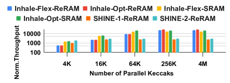
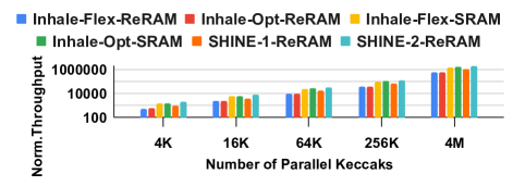
5.5. Performance Scaling
In this section, we study the scalability of different designs. To show the effect of more Keccak permutations on performance, we increase the number of parallel Keccaks to up to 4 million and evaluate the performance of Inhale and SHINE with and without power limitations. Fig. 6 depicts the throughput of different Inhale and SHINE designs, normalized to the throughput of the single SHINE-1, with and without power constraints. In the power-constrained scenario, we assume the maximum power of 75W for all the designs. This reduces the number of computational units that can be executed concurrently.
Without taking the power constraint into account, we assume that all the parallel Keccaks can operate in processing units of Inhale and SHINE in parallel without compromising the performance. In this scenario, the relationship between the performance of various designs is identical to that shown in Table 1, i.e., the throughput is proportional to the number of parallel Keccaks. In the power-constrained scenario, Inhale-Opt-SRAM has 2.9, 2.8, 1.1, 1.6, and 0.8 higher throughput than Inhale-Flex-ReRAM, Inhale-Opt-ReRAM, Inhale-Flex-SRAM, SHINE-1-ReRAM, and SHINE-2-ReRAM, respectively, when computing 4K Keccak permutations in parallel. However, when the number of parallel Keccaks reaches 4M, Inhale-Opt-SRAM cannot continue the linear increase of throughput due to the power constraint, while Inhale-Opt-ReRAM becomes the design with the highest throughput, and shows up to 1.3, 1.7, 1.3, 12, and 10 better throughput over Inhale-Flex-ReRAM, Inhale-Flex-SRAM, Inhale-Opt-SRAM, SHINE-1-ReRAM, and SHINE-2-ReRAM, due to its lowest power consumption per permutation.
6. Conclusion
In this paper, we propose Inhale, an in-SRAM hashing engine with four-fold latency, throughput, area, and energy benefits for accelerating SHA-3 on a CPU chip with narrowed trusted computing base. By leveraging compatible data alignment and efficient read/write strategy, Inhale can eliminate the majority of unnecessary shift operations with minimal hardware modification. Our evaluation results demonstrate significant throughput-per-area-per-energy (up to 172) over the state-of-the-art in-memory and ASIC solutions. Future work will extend Inhale to provide an end-to-end privacy-preserving solution for IoT devices.
References
- (1)
- Aga et al. (2017) Shaizeen Aga, Supreet Jeloka, Arun Subramaniyan, Satish Narayanasamy, David Blaauw, and Reetuparna Das. 2017. Compute caches. In 2017 IEEE International Symposium on High Performance Computer Architecture (HPCA).
- Akin et al. (2010) Abdulkadir Akin, Aydin Aysu, Onur Can Ulusel, and Erkay Savaş. 2010. Efficient hardware implementations of high throughput SHA-3 candidates keccak, luffa and blue midnight wish for single-and multi-message hashing. In Proceedings of the 3rd International Conference on Security of Information and Networks.
- Alagic et al. (2020) Gorjan Alagic, Jacob Alperin-Sheriff, Daniel Apon, David Cooper, Quynh Dang, John Kelsey, Yi-Kai Liu, Carl Miller, Dustin Moody, and Rene Peralta. 2020. Status report on the second round of the NIST post-quantum cryptography standardization process. US Department of Commerce, NIST (2020).
- Avanzi et al. (2019) Roberto Avanzi, Joppe Bos, Léo Ducas, Eike Kiltz, Tancrède Lepoint, Vadim Lyubashevsky, John M. Schanck, Peter Schwabe, Gregor Seiler, and Damien Stehlé. 2019. CRYSTALS-Kyber algorithm specifications and supporting documentation. NIST PQC Round (2019).
- Bhattacharjee et al. (2017) Debjyoti Bhattacharjee, Vikramkumar Pudi, and Anupam Chattopadhyay. 2017. SHA-3 implementation using ReRAM based in-memory computing architecture. In 2017 18th International Symposium on Quality Electronic Design (ISQED).
- Cawthra et al. (2020) Jennifer Cawthra, Michael Ekstrom, Lauren Lusty, Julian Sexton, John Sweetnam, and Anne Townsend. 2020. Data integrity: Identifying and protecting assets against ransomware and other destructive events. (2020).
- Costan and Devadas (2016) Victor Costan and Srinivas Devadas. 2016. Intel SGX explained. Cryptology ePrint Archive (2016).
- Dierks and Rescorla (2008) Tim Dierks and Eric Rescorla. 2008. The transport layer security (TLS) protocol version 1.2.
- Dworkin (2015) Morris J. Dworkin. 2015. SHA-3 standard: Permutation-based hash and extendable-output functions. (2015).
- Eckert et al. (2018) Charles Eckert, Xiaowei Wang, Jingcheng Wang, Arun Subramaniyan, Ravi Iyer, Dennis Sylvester, David Blaaauw, and Reetuparna Das. 2018. Neural cache: Bit-serial in-cache acceleration of deep neural networks. In 2018 ACM/IEEE 45Th annual international symposium on computer architecture (ISCA).
- Fujiki et al. (2019) Daichi Fujiki, Scott Mahlke, and Reetuparna Das. 2019. Duality cache for data parallel acceleration. In Proceedings of the 46th International Symposium on Computer Architecture.
- Guthaus et al. (2016) Matthew R. Guthaus, James E. Stine, Samira Ataei, Brian Chen, Bin Wu, and Mehedi Sarwar. 2016. OpenRAM: An open-source memory compiler. In 2016 IEEE/ACM International Conference on Computer-Aided Design (ICCAD). 1–6.
- Jeloka et al. (2016) Supreet Jeloka, Naveen Bharathwaj Akesh, Dennis Sylvester, and David Blaauw. 2016. A 28 nm configurable memory (TCAM/BCAM/SRAM) using push-rule 6T bit cell enabling logic-in-memory. IEEE Journal of Solid-State Circuits (2016).
- Jiang et al. (2020) Shunning Jiang, Peitian Pan, Yanghui Ou, and Christopher Batten. 2020. PyMTL3: A Python framework for open-source hardware modeling, generation, simulation, and verification. IEEE Micro 40, 4 (2020), 58–66.
- Kaplan et al. (2016) David Kaplan, Jeremy Powell, and Tom Woller. 2016. AMD memory encryption. White paper (2016).
- Madakam et al. (2015) Somayya Madakam, Vihar Lake, Vihar Lake, and Vihar Lake. 2015. Internet of Things (IoT): A literature review. Journal of Computer and Communications 3, 5 (2015), 164.
- Mahmoud et al. (2015) Rwan Mahmoud, Tasneem Yousuf, Fadi Aloul, and Imran Zualkernan. 2015. Internet of things (IoT) security: Current status, challenges and prospective measures. In 2015 10th international conference for internet technology and secured transactions (ICITST).
- Möser et al. (2017) Malte Möser, Kyle Soska, Ethan Heilman, Kevin Lee, Henry Heffan, Shashvat Srivastava, Kyle Hogan, Jason Hennessey, Andrew Miller, and Arvind Narayanan. 2017. An empirical analysis of traceability in the monero blockchain. arXiv preprint arXiv:1704.04299 (2017).
- Nagarajan et al. (2019) Karthikeyan Nagarajan, Sina Sayyah Ensan, Mohammad Nasim Imtiaz Khan, Swaroop Ghosh, and Anupam Chattopadhyay. 2019. SHINE: A novel SHA-3 implementation using ReRAM-based in-memory computing. In 2019 IEEE/ACM International Symposium on Low Power Electronics and Design (ISLPED).
- NXP (2022) NXP. 2022. LPC1225FBD48 | Arm Cortex-M0 | 32-bit MCU | NXP Semiconductors. Retrieved August 11, 2022 from https://www.nxp.com/products/processors-and-microcontrollers/arm-microcontrollers/general-purpose-mcus/lpc1200-cortex-m0/64-kb-flash-8-kb-sram-lqfp48-package:LPC1225FBD48
- Obiri et al. (2021) Isaac Amankona Obiri, Jingcong Yang, Qi Xia, and Jianbin Gao. 2021. A Sovereign PKI for IoT Devices Based on the Blockchain Technology. In 2021 18th International Computer Conference on Wavelet Active Media Technology and Information Processing (ICCWAMTIP).
- Pessl and Hutter (2013) Peter Pessl and Michael Hutter. 2013. Pushing the limits of SHA-3 hardware implementations to fit on RFID. In International Conference on Cryptographic Hardware and Embedded Systems.
- Poremba et al. (2015) Matt Poremba, Sparsh Mittal, Dong Li, Jeffrey S. Vetter, and Yuan Xie. 2015. Destiny: A tool for modeling emerging 3d nvm and edram caches. In 2015 Design, Automation & Test in Europe Conference & Exhibition (DATE).
- Ramanarayanan et al. (2010) Rajaraman Ramanarayanan, Sanu Mathew, Farhana Sheikh, Suresh Srinivasan, Amit Agarwal, Steven Hsu, Himanshu Kaul, Mark Anders, Vasantha Erraguntla, and Ram Krishnamurthy. 2010. 18Gbps, 50mW reconfigurable multi-mode SHA Hashing accelerator in 45nm CMOS. In 2010 Proceedings of ESSCIRC.
- Reis et al. (2022) Dayane Reis, Haoran Geng, Michael Niemier, and Xiaobo Sharon Hu. 2022. IMCRYPTO: An In-Memory Computing Fabric for AES Encryption and Decryption. IEEE Transactions on Very Large Scale Integration (VLSI) Systems (2022).
- Singla and Bertino (2018) Ankush Singla and Elisa Bertino. 2018. Blockchain-based PKI solutions for IoT. In 2018 IEEE 4th International Conference on Collaboration and Internet Computing (CIC).
- Subramaniyan et al. (2017) Arun Subramaniyan, Jingcheng Wang, Ezhil RM Balasubramanian, David Blaauw, Dennis Sylvester, and Reetuparna Das. 2017. Cache automaton. In Proceedings of the 50th Annual IEEE/ACM International Symposium on Microarchitecture.
- Tillich et al. (2009) Stefan Tillich, Martin Feldhofer, Mario Kirschbaum, Thomas Plos, Jörn-Marc Schmidt, and Alexander Szekely. 2009. High-speed hardware implementations of blake, blue midnight wish, cubehash, echo, fugue, grøstl, hamsi, jh, keccak, luffa, shabal, shavite-3, simd, and skein. Cryptology EPrint Archive (2009).
- Won et al. (2018) Jongho Won, Ankush Singla, Elisa Bertino, and Greg Bollella. 2018. Decentralized public key infrastructure for internet-of-things. In MILCOM 2018-2018 IEEE Military Communications Conference (MILCOM).
- Wong et al. (2018) Ming Ming Wong, Jawad Haj-Yahya, Suman Sau, and Anupam Chattopadhyay. 2018. A new high throughput and area efficient SHA-3 implementation. In 2018 IEEE International Symposium on Circuits and Systems (ISCAS).
- Wood (2014) Gavin Wood. 2014. Ethereum: A secure decentralised generalised transaction ledger. Ethereum project yellow paper (2014).
- Zhang et al. (2022) Jingyao Zhang, Hoda Naghibijouybari, and Elaheh Sadredini. 2022. Sealer: In-SRAM AES for High-Performance and Low-Overhead Memory Encryption. In Proceedings of the ACM/IEEE International Symposium on Low Power Electronics and Design.
- Zhang et al. (2018a) Wei Zhang, Pengfei Wang, Xiao Li, and Dehua Shen. 2018a. Some stylized facts of the cryptocurrency market. Applied Economics (2018).
- Zhang et al. (2018b) Yiqun Zhang, Li Xu, Qing Dong, Jingcheng Wang, David Blaauw, and Dennis Sylvester. 2018b. Recryptor: A reconfigurable cryptographic cortex-M0 processor with in-memory and near-memory computing for IoT security. IEEE Journal of Solid-State Circuits (2018).