Further author information:
E. D. Miller: E-mail: milleric@mit.edu
Understanding the effects of charge diffusion in next-generation soft X-ray imagers
Abstract
To take advantage of high-resolution optics sensitive to a broad energy range, future X-ray imaging instruments will require thick detectors with small pixels. This pixel aspect ratio affects spectral response in the soft X-ray band, vital for many science goals, as charge produced by the photon interaction near the entrance window diffuses across multiple pixels by the time it is collected, and is potentially lost below the imposed noise threshold. In an effort to understand these subtle but significant effects and inform the design and requirements of future detectors, we present simulations of charge diffusion using a variety of detector characteristics and operational settings, assessing spectral response at a range of X-ray energies. We validate the simulations by comparing the performance to that of real CCD detectors tested in the lab and deployed in space, spanning a range of thickness, pixel size, and other characteristics. The simulations show that while larger pixels, higher bias voltage, and optimal backside passivation improve performance, reducing the readout noise has a dominant effect in all cases. We finally show how high-pixel-aspect-ratio devices present challenges for measuring the backside passivation performance due to the magnitude of other processes that degrade spectral response, and present a method for utilizing the simulations to qualitatively assess this performance. Since compelling science requirements often compete technically with each other (high spatial resolution, soft X-ray response, hard X-ray response), these results can be used to find the proper balance for a future high-spatial-resolution X-ray instrument.
keywords:
X-ray detectors, CCDs, charge diffusion, detector response1 Introduction
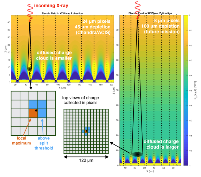
Future silicon-based soft X-ray imaging instruments will require small pixels to take advantage of advanced high-resolution optics, while also greatly benefiting from thick detector bulk to maximize the sensitive band-pass. For example, the wide-field imaging detectors baselined for both the AXIS Probe-class mission concept[1] and the Lynx Great Observatory concept[2] require 16-m pixels to properly sample the PSF goal, yet they need to be backside-illuminated devices fully depleted to 100 m to provide sufficient quantum efficiency over the full 0.2–12 keV band. This pixel aspect ratio of 6:1 is unprecedented among similar X-ray instruments, which are closer to 2:1 for Chandra ACIS-S3 and Suzaku XIS1. “Taller” pixels allow for more lateral diffusion of the X-ray-induced photoelectrons as they drift toward the collection gates under influence of the bias electric field, as demonstrated schematically in Figure 1. This diffusion is greatest for soft photons which interact with the silicon bulk near the entrance window, and since these photons also produce fewer photoelectrons than their harder counterparts, charge can be spread out across many pixels and potentially lost below the imposed noise thresholds, having substantial effects on the overall soft X-ray response. Here “response” refers to the combined effects of our ability (or lack thereof) to reconstruct the energy of individual detected photons, and mainly includes the spectral resolution FWHM, knowledge of the energy scale, and reduced quantum efficiency due to events lost below the noise threshold.
It is at the softest energies where some of the most ground-breaking high-energy astrophysics will be done, including probing the seeds of the first supermassive black holes at high redshift, tracing the faintest hot gas in the outskirts of galaxy clusters and the tenuous intergalactic medium, and understanding the role of stellar and AGN feedback in shaping galaxies like our own Milky Way[1, 2]iiiSee the Concept Study Reports for Lynx (https://wwwastro.msfc.nasa.gov/lynx/docs/LynxConceptStudy.pdf) and AXIS (https://smd-prod.s3.amazonaws.com/science-red/s3fs-public/atoms/files/AXIS_Study_Rpt.pdf).. For these reasons, understanding the processes governing the movement of charge in silicon detectors is an area of active research.[3, 4, 5, 6, 7, 8] In this work, we extend our recent investigation of charge diffusion[7] in real detectors under development for strategic missions like AXIS and Lynx[9] by using simulations. These are validated with real data from different sources, and we use the results to explore the effects of different detector design parameters on the X-ray response across a range of energies from 0.3 to 6 keV. We emphasize that these results are applicable to any silicon-based X-ray imager, including CCDs[9], CMOS devices[10], and DEPFETs[11].
2 Simulations and data analysis
2.1 Simulating the detector electric field and charge diffusion
We performed simulations using Poisson CCD [12], a software package that, given a set of structural and operational characteristics for the detector, (1) solves Poisson’s equation for the electric field in three dimensions at all points within the detector volume, and (2) tracks the drift and diffusion of electrons placed within this volume until they reach the buried channel, where they are collected in pixels defined by the channel stop and barrier gate fields. The simulated detector is a backside-illuminated, 100-m thick CCD with 8-m pixels, a three-phase gate structure with one collecting gate held at +1.5 V and two barrier gates held at 1.5 V, and implant structure and doping levels based on the MIT Lincoln Lab CCID-93 device described in our recent comparison of lab data and simulation[7]. The simulation volume covered 99 pixels, with non-linear electric field grid spacing in the vertical direction allowing finer grid sampling of 30 nm at the front and back sides of the device to properly capture the electric field structure, and coarser grid sampling (up to 300 nm) throughout the bulk of the device. The electric field was simulated at an operating temperature of C at substrate bias voltages of , , and V, all sufficient to fully deplete the silicon bulk and eliminate field-free regions. Examples of vertical electric field structure resulting such simulations are shown in Figure 1.
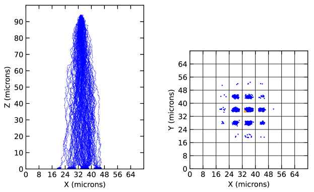
Charge diffusion was simulated for each using 100,000 photons each at energies of 5.89 keV (Mn K), 1.25 keV (Mg K), 0.525 keV (O K), and 0.277 keV (C K). This was done by introducing small clouds of electrons into the simulated detector volume and allowing them to drift and diffuse under the influence of the 3-D electric field until collected in pixels. The number of electrons in each cloud was drawn from a Fano noise distribution appropriate for the photon energy in Si (e.g., 161514 electrons for 5.9 keV), and the interaction depth was drawn from an exponential distribution with appropriate energy-dependent attenuation length. Each interaction location was generated from a uniform distribution across the central pixel of the 99-pixel simulation volume. An example diffusion run is shown in Figure 2.
We simulated the quality of backside passivation by adjusting the TopAbsorptionProb parameter, which is the probability that a diffused photoelectron encountering the backside entrance window is absorbed rather than reflected back into the bulk; this ranged from 0% (perfect passivation) to 25%. The final pixelized 2-D spatial distribution of electrons was binned 22 and 33 to simulate 16-m and 24-m pixels, respectively; although this is technically different than simulating drift and diffusion in a detector with the correct pixel size, it greatly reduced the required simulation time, and several test runs showed there was no noticeable difference between the methods, as the majority of the diffusion occurs in the bulk before the charge cloud feels the effects of the gate barrier and channel stop electric fields (see Figures 1 and 2, left panel). Finally, Gaussian readout noise ranging from 1 to 4 e- RMS was added to each pixel, and event detection and characterization were performed in the same way as flight software on Chandra ACIS and Suzaku XIS, as described in our previous work.[7] For each single-photon frame, we used a 5 threshold for event candidate identification, and summed all pixels including neighbors above 4 to calculate the total event energy. These thresholds are similar to values tuned for previous instruments to eliminate noise events and inclusion of noisy pixels in event pulse height summation. At a temperature of C, we expect a conversion of 3.71 eV per e-[13], and so in the highest noise case of 4 e- RMS, the event threshold corresponds to 74 eV and the neighbor (or “split”) threshold to 59 eV. These are high enough to lose a significant fraction of the signal in a low-energy event split over several pixels. In addition, a 5 event threshold has a 25% chance of introducing a noise event in a 1-Mpix array; for the expected 20 fps frame rate for a mission like AXIS, this will introduce many such events, and thus an event threshold that is many factors of the readout noise and still well below the science band of interest is desirable.
As also discussed in our previous work[7], the default charge diffusion parameters in Poisson CCD produced much more diffusion in the simulations than we observe in the lab data, with much larger event sizes. We used similar DiffMultiplier parameter values that produced simulated event size distributions closely matched to the real data, and also similar to values supported by theoretical studies. The validation with real data presented in our previous work and here in Section 2.2 support use of this diffusion factor, and in fact more diffusion would magnify the importance of factors such as readout noise, pixel size, and bias voltage in the resultant soft response. The slight discrepancy between our tuned DiffMultiplier value and the expected value will be explored in a future paper.
2.2 Validation of simulations with real data
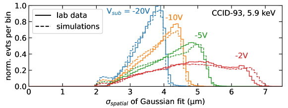
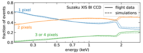
To validate the simulations, we simulated charge diffusion in two real X-ray detectors for which we have substantial data, both BI CCDs fabricated by MIT Lincoln Laboratory: the CCID-93 small-format, small-pixel (8-m) device[7]; and the CCID-41 device flown as Suzaku XIS1[14]. The CCID-93 simulations are similar to the unbinned 5.9-keV runs described in Section 2.1, although with 50-m thickness, and as in our previous work[7], we fit 2-D Gaussians to pixelated event islands to measure the charge diffusion. As shown in the top panel of Figure 3, the simulated sizes match the lab data very well. The Suzaku data includes flight data from a number of bright, un-piled sources, including the Perseus Cluster and the bright blazars PKS 2155 and 3C 273, the latter taken in 1/8 window mode. This data from these bright continuum sources is dominated by X-ray photons across a wide energy band, with very little contamination from particle events. We parametrize charge diffusion using the ASCA grade specifying how many pixels in an event are above the noise threshold. As shown in the bottom panel of Figure 3, the simulations match the observed charge diffusion exceptionally well at soft energies. While both real devices are 50 m thick, about half that of the notional simulated detector, the dependence of diffusion with drift distance is well-defined, and this validation gives us confidence that our simulation results are reliable.
3 Results
3.1 Spectral response
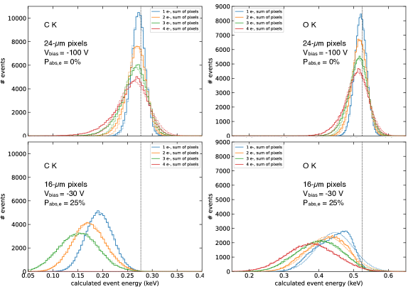
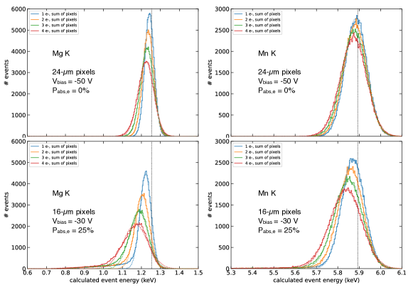
The effects of charge diffusion on spectral response are apparent in all of our simulations. Figures 4 and 5 show histograms of reconstructed event energy for the four monochromatic energies under study: C K (0.28 keV), O K (0.53 keV), Mg K (1.25 keV), and Mn K (5.9 keV). Colors show results for different values of readout noise, ranging from 1 to 4 e- RMS. In each figure, an “ideal” detector from the standpoint of maximizing charge collection is shown in the top panels. A lower performance but still realistic detector is represented in the lower panels. Pixel size, substrate bias voltage, and back surface passivation quality contribute to the width and shape of the response. These effects are greatest at low energies, where peak energy shifts and non-Gaussian shapes appear even for low readout noise. Quantum efficiency (QE) is affected as well, in the worst case resulting in no events being detected for C K with 4 e- RMS noise (Figure 4, lower left).
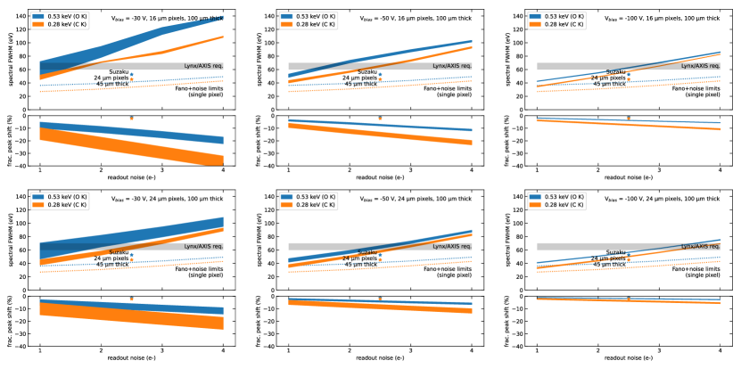
Each spectral histogram in Figure 4 and 5 was fit with a simple Gaussian to estimate the spectral resolution FWHM and the peak energy shift. These are shown in Figure 6, with top and bottom panels showing different pixel sizes, and substrate bias voltage increasing from right to left. In effect, the upper left panel is the lower performance detector, and the bottom right panel is the ideal. Colored bands show the range of FWHM and peak shift for a range of “good” backside passivation. In all cases, readout noise of 2–3 e- or lower is necessary to meet the spectral resolution requirements of a mission like AXIS, shown by the gray band. Even at this level, there is little allowance for additional FWHM degradation that may be caused by (for example) poorer backside treatment or charge-transfer inefficiency (CTI) in CCDs[15].
3.2 Assessing the back surface quality
To maximize QE at X-ray photon energies where the attenuation length in silicon is very short (0.5 m below 0.5 keV), X-ray imagers must be thinned, fully depleted, and illuminated on the backside. The thinning process introduces open bonds on the surface that can absorb photoelectrons, and for this and other reasons the surface must be passivated by introducing a thin layer of dopant. The CCID-93 device currently under study uses molecular beam epitaxy (MBE) to introduce this layer[17], and its effectiveness at passivating the surface is of great interest as the science goals of future strategic missions demand good soft X-ray QE and spectral resolution.
As we have shown, a large number of factors contribute to the overall detector response, and these can be difficult to separate from each other in lab data. The simulations we have presented here provide a method for doing just that, since we can easily change the magnitude of these various factors, and since they have been validated for a real-life instrument with exquisite soft response (see Figure 3). To demonstrate this, we have used the 1 e- RMS readout noise, 16-m pixel, V simulations in an attempt to quantify the fraction of photons that suffer charge loss at the entrance surface. As described in Section 2.1, the backside quality is captured in Poisson CCD in a parameter called TopAbsorptionProb, the probability that a photoelectron encountering the entrance window will be absorbed and thus lost from the charge packet created by the X-ray. We show in Figure 7 monoenergetic spectra for these simulations at three energies (columns) and for four values of the backside quality (rows). Perfect passivation (TopAbsorptionProb = 0%) is shown at the top, and we fit each of these spectra with a single Gaussian, which is a good fit. For the poorer passivation simulations (TopAbsorptionProb 0%), we introduce two Gaussians; the first, shown in blue, represents events that have no surface losses, and in these fits the and mean are fixed to the perfect passivation Gaussian from the top panel. The second, orange Gaussian represents the ensemble of events that have lost some fraction of charge to the surface, and this is allowed to fit freely. The blue Gaussian amplitude is allowed to vary to account for events that migrate to this ensemble.
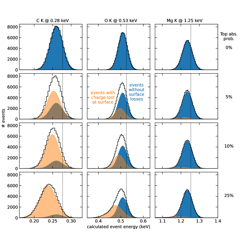
At the lowest energy of 0.28 keV, where the attenuation length is only 0.11 m, even a mild decrease in passivation quality results in a majority of photons losing some charge to the surface: 64% for 5% absorption probability, and 93% for 25%. At 0.53 keV and 0.49 m attenuation length, the non-Gaussianity of the response is easier to see, and about half of the photons lose charge to the surface in the 25% absorption probably case. At 1.25 keV, the attenuation length is 5 m, and while a low-energy tail can be seen, only about 6% of photons are contained in the orange Gaussian and thus identified as losing charge to the surface. This fraction is the same for all absorption probabilities, and may indicate something physical or a limitation of this technique for photon ensembles which have a range of penetration depths extending well into the silicon bulk. The results for 5.9 keV are not shown, as with a 29-m attenuation length there is little surface loss; the vast majority of photons interact away from the surface and have their charge quickly caught up in the bias-induced drift.
We have used the 1 readout noise simulations in this test case because it is easiest to see the effects of backside quality when it dominates the response broadening compared to other factors. In future work, we will expand this method to more demanding cases with higher noise and other factors that degrade resolution, such as CTI. We will also explore a more physical and quantitative method of assessing the backside quality and other surface effects than the simplified TopAbsorptionProb parameter. In particular, we don’t expect real events with lost charge to follow a Gaussian distribution, but rather have an extended non-Gaussian or even constant tail to lower energies. The Gaussianity is likely an artifact of this simplified probabilistic charge loss that ignores (for example) initial high-energy photoelectrons completely leaving the silicon. We will also probe the dependence at different energies and as a function of interaction depth of individual photons rather than as an ensemble.
4 Summary
We have simulated charge diffusion in thick, small-pixel, back-illuminated silicon X-ray imagers to understand the effects on soft X-ray response. The simulations show that, while larger pixels, higher bias voltage, and optimal backside passivation improve performance, reducing the readout noise has a dominant effect in all cases. Since compelling science requirements often compete technically with each other (high spatial resolution, soft X-ray response, hard X-ray response), these results can be used to find the proper balance for a future high-spatial-resolution X-ray instrument.
This variety of response-degrading effects in such detectors complicates assessment of the backside passivation quality, vital for the good soft X-ray response demanded by the science goals of future strategic missions. We have presented a method to qualitatively assess the backside treatment, using our validated simulations to estimate the relative size of the ensembles of photons that lose charge to the surface and those that do not. We will explore this more in future work, with the aim of developing a spectral resolution budget that can be adapted to help formulate future mission requirements.
Acknowledgements.
We gratefully acknowledge support from NASA through the Strategic Astrophysics Technology (SAT) program, grants 80NSSC18K0138 and 80NSSC19K0401 to MIT, and from the Kavli Research Infrastructure Fund of the MIT Kavli Institute for Astrophysics and Space Research.References
- [1] Mushotzky, R., “AXIS: a probe class next generation high angular resolution x-ray imaging satellite,” in [Space Telescopes and Instrumentation 2018: Ultraviolet to Gamma Ray ], Proc. SPIE 10699 (August 2018).
- [2] Gaskin, J. A., Allured, R., Bandler, S. R., Basso, S., Bautz, M. W., Baysinger, M. F., Biskach, M. P., Boswell, T. M., Capizzo, P. D., Chan, K.-W., Civitani, M. M., Cohen, L. M., Cotroneo, V., Davis, J. M., DeRoo, C. T., DiPirro, M. J., Dominguez, A., Fabisinski, L. L., Falcone, A. D., Figueroa-Feliciano, E., Garcia, J. C., Gelmis, K. E., Heilmann, R. K., Hopkins, R. C., Jackson, T., Kilaru, K., Kraft, R. P., Liu, T., McClelland, R. S., McEntaffer, R. L., McCarley, K. S., Mulqueen, J. A., Özel, F., Pareschi, G., Reid, P. B., Riveros, R. E., Rodriguez, M. A., Rowe, J. W., Saha, T. T., Schattenburg, M. L., Schnell, A. R., Schwartz, D. A., Solly, P. M., Suggs, R. M., Sutherlin, S. G., Swartz, D. A., Trolier-McKinstry, S., Tutt, J. H., Vikhlinin, A., Walker, J., Yoon, W., and Zhang, W. W., “Lynx Mission concept status,” in [Society of Photo-Optical Instrumentation Engineers (SPIE) Conference Series ], Society of Photo-Optical Instrumentation Engineers (SPIE) Conference Series 10397, 103970S (Sept. 2017).
- [3] Prigozhin, G., Butler, N. R., Kissel, S. E., and Ricker, G. R., “An experimental study of charge diffusion in the undepleted silicon of X-ray CCDs,” IEEE Transactions on Electron Devices 50, 246–253 (Jan. 2003).
- [4] Miller, E. D., Foster, R., Lage, C., Prigozhin, G., Bautz, M., Grant, C., LaMarr, B., and Malonis, A., “The effects of charge diffusion on soft x-ray response for future high-resolution imagers,” in [Society of Photo-Optical Instrumentation Engineers (SPIE) Conference Series ], Society of Photo-Optical Instrumentation Engineers (SPIE) Conference Series 10699, 106995R (July 2018).
- [5] Haro, M. S., Fernandez Moroni, G., and Tiffenberg, J., “Studies on small charge packet transport in high-resistivity fully depleted ccds,” IEEE Transactions on Electron Devices 67(5), 1993–2000 (2020).
- [6] Prigozhin, I., Dominici, S., and Bellotti, E., “Fbmc3d—a large-scale 3-d monte carlo simulation tool for modern electronic devices,” IEEE Transactions on Electron Devices 68(1), 279–287 (2021).
- [7] LaMarr, B. J., Prigozhin, G. Y., Miller, E. D., Thayer, C., Bautz, M. W., Foster, R., Grant, C. E., Malonis, A., Burke, B. E., Cooper, M., Donlon, K., and Leitz, C., “Measurement and simulation of charge diffusion in a small-pixel charge-coupled device,” Journal of Astronomical Telescopes, Instruments, and Systems 8, 016004 (Jan. 2022).
- [8] Avalos, N. E. and Sofo Haro, M., “G-CoReCCD: a GPU-based simulator of the charge transport in fully-depleted CCDs,” in [SPIE Future Sensing Technologies ], Society of Photo-Optical Instrumentation Engineers (SPIE) Conference Series 11525, 115250I (Nov. 2020).
- [9] Bautz, M. W., Foster, R., Grant, C. E., LaMarr, B., Malonis, A., Miller, E. D., Prigozhin, G., Burke, B., Cooper, M., Donlon, K., Lambert, R., Warner, K., Young, D., Chattopadhyay, T., Herrmann, S., Morris, R. G., Leitz, C., and Allen, S., “Performance of high frame-rate CCDs for future strategic missions,” in [Space Telescopes and Instrumentation 2022: Ultraviolet to Gamma Ray ], Society of Photo-Optical Instrumentation Engineers (SPIE) Conference Series 12181, 12181–85 (2022).
- [10] Chattopadhyay, T., Falcone, A. D., Burrows, D. N., Hull, S., Bray, E., Wages, M., McQuaide, M., Buntic, L., Crum, R., O’Dell, J., and Anderson, T., “X-ray hybrid CMOS detectors: recent development and characterization progress,” in [Space Telescopes and Instrumentation 2018: Ultraviolet to Gamma Ray ], Society of Photo-Optical Instrumentation Engineers (SPIE) Conference Series 10699, 106992E (July 2018).
- [11] Meidinger, N., Barbera, M., Emberger, V., Fürmetz, M., Manhart, M., Müller-Seidlitz, J., Nandra, K., Plattner, M., Rau, A., and Treberspurg, W., “The Wide Field Imager instrument for Athena,” Proc. SPIE 10397, 103970V (Aug. 2017).
- [12] Lage, C., Bradshaw, A., Anthony Tyson, J., and LSST Dark Energy Science Collaboration, “Poisson_CCD: A dedicated simulator for modeling CCDs,” Journal of Applied Physics 130, 164502 (Oct. 2021).
- [13] Groom, D. E., Bebek, C. J., Fabricius, M., Karcher, A., Kolbe, W. F., Roe, N. A., and Steckert, J., “Quantum efficiency characterization of LBNL CCD’s: Part I. The quantum efficiency machine,” in [Sensors, Cameras, and Systems for Scientific/Industrial Applications VII ], Blouke, M. M., ed., Society of Photo-Optical Instrumentation Engineers (SPIE) Conference Series 6068, 133–143 (Feb. 2006).
- [14] Koyama, K., Tsunemi, H., Dotani, T., Bautz, M. W., Hayashida, K., Tsuru, T. G., Matsumoto, H., Ogawara, Y., Ricker, G. R., Doty, J., Kissel, S. E., Foster, R., Nakajima, H., Yamaguchi, H., Mori, H., Sakano, M., Hamaguchi, K., Nishiuchi, M., Miyata, E., Torii, K., Namiki, M., Katsuda, S., Matsuura, D., Miyauchi, T., Anabuki, N., Tawa, N., Ozaki, M., Murakami, H., Maeda, Y., Ichikawa, Y., Prigozhin, G. Y., Boughan, E. A., Lamarr, B., Miller, E. D., Burke, B. E., Gregory, J. A., Pillsbury, A., Bamba, A., Hiraga, J. S., Senda, A., Katayama, H., Kitamoto, S., Tsujimoto, M., Kohmura, T., Tsuboi, Y., and Awaki, H., “X-Ray Imaging Spectrometer (XIS) on Board Suzaku,” PASJ 59, 23–33 (Jan. 2007).
- [15] LaMarr, B., Bautz, M., Miller, E., Prigozhin, G., Foster, R., Cooper, M., and Donlon, K., “Charge transfer efficiency of CCDs with a single-polysilicon gate structure,” in [X-Ray, Optical, and Infrared Detectors for Astronomy X ], Society of Photo-Optical Instrumentation Engineers (SPIE) Conference Series 12191, 12191–89 (2022).
- [16] Bautz, M. W., Kissel, S. E., Prigozhin, G. Y., LaMarr, B., Burke, B. E., and Gregory, J. A., “Progress in x-ray CCD sensor performance for the Astro-E2 X-ray imaging spectrometer,” in [Society of Photo-Optical Instrumentation Engineers (SPIE) Conference Series ], A. D. Holland, ed., Society of Photo-Optical Instrumentation Engineers (SPIE) Conference Series 5501, 111–122 (Sept. 2004).
- [17] Ryu, K. K., Leitz, C. W., Clark, H. R., Chen, X., Cooper, M. J., Zhu, M., Welander, P. B., Lambert, R. D., Bolkhovsky, V., Yost, D. R. W., Burke, B. E., Gregory, J. A., and Suntharalingam, V., “Oxide-bonded molecular-beam epitaxial backside passivation process for large-format CCDs,” in [Space Telescopes and Instrumentation 2018: Ultraviolet to Gamma Ray ], den Herder, J.-W. A., Nikzad, S., and Nakazawa, K., eds., Society of Photo-Optical Instrumentation Engineers (SPIE) Conference Series 10699, 106993P (July 2018).