Large spin Hall conductivity and excellent hydrogen evolution reaction activity in unconventional PtTe1.75 monolayer
Abstract
Two-dimensional (2D) materials have gained lots of attention due to the potential applications. In this work, we propose that based on first-principles calculations, the (22) patterned PtTe2 monolayer with kagome lattice formed by the well-ordered Te vacancy (PtTe1.75) hosts large spin Hall conductivity (SHC) and excellent hydrogen evolution reaction (HER) activity. The unconventional nature relies on the band representation (BR) of the highest valence band without SOC. The large SHC comes from the Rashba spin-orbit coupling (SOC) in the noncentrosymmetric structure induced by the Te vacancy. Even though it has a metallic SOC band structure, the invariant is well defined due to the existence of the direct band gap and is computed to be nontrivial. The calculated SHC is as large as 1.25 at the Fermi level (). By tuning the chemical potential from to eV, it varies rapidly and monotonically from to 3.1. In addition, we also find the Te vacancy in the patterned monolayer can induce excellent HER activity. Our results not only offer a new idea to search 2D materials with large SHC, i.e., by introducing inversion-symmetry breaking vacancies in large SOC systems, but also provide a feasible system with tunable SHC (by applying gate voltage) and excellent HER activity.
I Introduction
In the past decade, many topological semimetals with various quasi-particle dispersions and fascinating properties have been proposed Armitage et al. (2018); Wan et al. (2011); Wang et al. (2013); Bradlyn et al. (2016); Wieder et al. (2016). The layered noble transition-metal dichalcogenide PtTe2 is extraordinary with heavily tilted type-II Dirac fermion Yan et al. (2017). It hosts unique properties, such as topological nontrivial band structure Yan et al. (2017); Politano et al. (2018), ultrahigh electrical conductivity Fu et al. (2018); Hao et al. , and robustness of the remaining semimetal phase even down to just two triatomic layers Lin et al. (2020); Deng et al. (2019). Soon after, many PtTe2 derivatives have been proposed, including the monolayer, multilayer, doping, vacancy, heterojunction structures and so on. For example, the Ir-doped PtTe2 (i.e., Pt1-xIrxTe2) has realized the Fermi level () tunability and superconductivity, which opens up a new route for the investigation of Dirac physics and topological superconductivity Fei et al. ; Jiang et al. (2020); Nie et al. (2018). More recently, PtTe2-based broadband photodetectors and image sensors have been fabricated, demonstrating tremendous potential application value in various photoelectric devices Tong et al. (2020); Shawkat et al. (2021); Xu et al. . Very recently, the patterned monolayer with kagome lattice formed by one Te vacancy in the supercell has been grown successfully Liu et al. (2021), whose band topology and potential properties are unknown. The study of PtTe2 derivatives can not only reveal novel condensed matter physics but also facilitate the versatile development in device physics.
In this work, we theoretically propose that the recently synthesized patterned PtTe2 monolayer with the Te vacancy hosts large SHC due to the Rashba SOC, where the Te vacancy breaks inversion symmetry (). The momentum offset and strength of the Rashba SOC are estimated, Å-1 and eV Å. The momentum offset is very large and comparable with the largest one reported in the Bi/Ag(111) surface alloy in literature Ast et al. (2007), which induces visible Rashba band splitting. Using the Kubo formula approach at the clean limit, we find the Rashba SOC will induce large SHC, as large as 1.25 at . Furthermore, the SHC changes rapidly and monotonically as the chemical potential evolving in a wide range ( eV), which benefits to the potential applications in spintronics. In the end, the variation of the Gibbs free energy for hydrogen adsorption progress is considered, which indicates that the Te vacancy can induce a superior HER activity.
II Crystal structure and Methodology
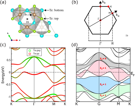
The pristine PtTe2 crystallizes in the CdI2-type trigonal () structure with space group (SG). It hosts the layered structure stacking along the axis. The patterned monolayer with kagome lattice formed by one Te vacancy in the 22 supercell has been successfully grown on the Pt(111) surface Liu et al. (2021). As shown in Fig. 1(a), the patterned PtTe2 monolayer (i.e., PtTe1.75) contains two Te layers: four Te atoms (blue balls) in the bottom layer and three Te atoms (green balls; with one vacancy schematized by “” at Wyckoff site) in the top layer. The distance between the bottom and top layers is Å. The Te vacancy breaks , resulting in a noncentrosymmetrical structure with p3m1 layer group (LG 69; corresponding to SG excluding translational symmetry along the axis). Thus, the Rashba SOC induced band splitting is inevitable. The lattice parameters and atomic positions are listed in Table S1 [in Section A of the Supplemental Material (SM A)].
We performed the first-principles calculations based on the density functional theory (DFT) using projector augmented wave (PAW) method Blöchl (1994); Kresse and Joubert (1999) implemented in the Vienna ab initio simulation package (VASP) Kresse and Furthmüller (1996a, b). The generalized gradient approximation (GGA) with exchange-correlation functional of Perdew, Burke and Ernzerhof (PBE) for the exchange-correlation functional Perdew et al. (1996) was adopted. The kinetic energy cutoff was set to 500 eV for the plane wave bases. The thickness of the vacuum layer along axis was set to Å. The BZ was sampled by -centered Monkhorst-Pack method with a 12121 k-mesh for the 2D periodic boundary conditions in the self-consistent process. The Wilson-loop technique Yu et al. (2011) was used to calculate the topological invariant. In addition, the electronic structures near were doubly checked by the full-potential local-orbital code (FPLO) Koepernik and Eschrig (1999) and fully consistent with that from VASP. The wannier-based tight-binding (TB) model under bases of the Te- and Pt- orbitals is extracted from the DFT calculations for the calculations of SHC.
III Calculations and Results
III.1 Electronic band structures
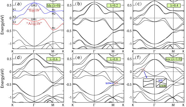
The band structures without and with SOC are presented in Fig. 1(c) and Fig. 1(d), respectively. Comparing them, we notice that the band dispersions change largely once including SOC. The most remarkable difference is that each band without SOC splits into two bands when SOC is considered. It is the Te vacancy in the monolayer which breaks (and ) inducing the visible Rashba band splitting. From the orbital-resolved band structures without SOC in Fig. 1(c), we find there exist visible band hybridizations between Te- and Te- orbitals around . Using IRVSP Gao et al. (2021a), the irreducible representations of the high-symmetry k points are calculated and labeled in Fig. 2(a). Accordingly, the BR analyses indicate that the two conduction bands belong to BR, while the highest valence band belongs to BR, suggesting the unconventional nature/obstructed atomic limit Nie et al. (2021a, b); Gao et al. (2022); Xu et al. (2021a).
SOC often plays important roles to engineering topological states, such as quantum spin Hall effect in graphene Kane and Mele (2005a, b) and Ta2M3Te5 (M=Pd,Ni) compounds Guo et al. (2021); Wang et al. (2021), 3D large-SOC-gap topological insulator in Bi2Se3 and NaCaBi families Zhang et al. (2009); Shao et al. (2021), and so on. In terms of the the patterned PtTe2 monolayer, once including SOC, the Te- dominated band around splits due to the Rashba SOC induced by the Te vacancy, as shown in Fig. 1(d). To get more insights in the nontrivial band topology and Rashba SOC band splitting, we have explored how the band structure evolves with the increasing strength of SOC (denoted by ) gradually in Fig. 2. We notice that the nontrivial band topology for occupied bands is due to the SOC (can be infinitesimal) induced band gap at without involving band inversion Bradlyn et al. (2017); Deng et al. (2022). In addition, the nontrivial topologies for and occupied bands are due to a gap closing and reopening process as varing . Taking occupied bands as an example, the critical Weyl band crossing between the th band and the th band appears on the M--K line with , as highlighted by a red dashed ring in Fig. 2(e). Similarly, the WP between the th band and the th band appears on the K-- line with , as the right inset shown in Fig. 2(f). However, it becomes topologically trivial for occupied bands since there are two nontrivial gap openings around both and M.
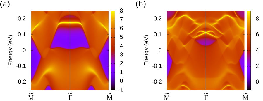
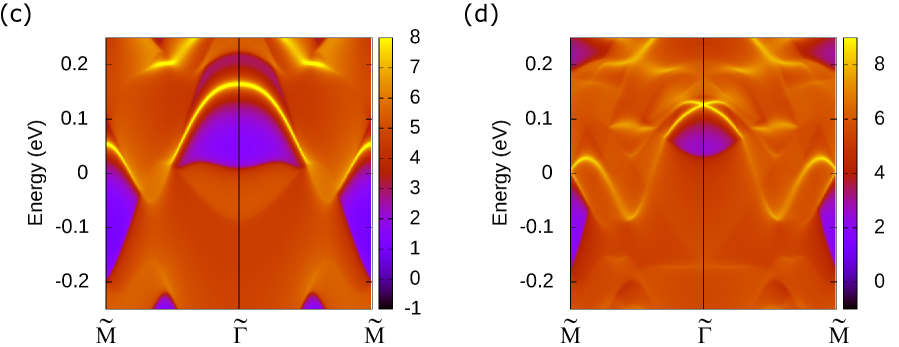
Since the existence of and symmetries, both the two classes of WPs above mentioned appear in sextuplet in the first BZ, as shown in Fig. 3(a) and Fig. 3(b). Similar with WPs in 3D Weyl semimetals Qian et al. (2020); Gao et al. (2021b); Nie et al. (2020); Shi et al. (2021), these critical WPs also conform to the codimensional analyses. This can be deduced as follows. First, both the M--K () and K-- () lines are invariant. In the two-band k p Hamiltonian depicting the Weyl band crossing, the combined antiunitary symmetry with will reduce the number of the independent matrices in the k p Hamiltonian to two. Second, the value in both the invariant lines and the SOC strength are two tunable parameters to search a WP. Thus, the number of the independent matrices in the k p Hamiltonian equals to the number of the tunable parameters, which indicates that a WP is stable in the 2D parameter space . In other words, a topological phase transition can happen by tuning in the invariant lines. Through the gap closing and reopening process in the evolution, it becomes topologically nontrivial for occupied bands. As a result, we can expected the existence of the helical edge states of the patterned PtTe2 monolayer. The edge spectra are presented in Fig. S3(b,d) [in Section C of the SM (SM C)].
III.2 Rashba SOC at
Because the Te vacancy breaks in the patterned PtTe2 monolayer, the Rashba SOC band splitting will appear inevitably. As the projected band structures with SOC shown in Fig. 3(c), the Te- dominated parabolic bands splits clearly near . The splitting bands near can be well fitted by with ( denoting the free electronic mass) and Å-1 (the momentum offset), as the two blue parabolas shown in Fig. 3(c). The coupling strength of the Rashba SOC can be derived as eVÅ. The estimated is super large in Fig. 3(c), as large as the the Bi/Ag(111) surface alloy Ast et al. (2007).

III.3 Large SHC effect
To explore the intrinsic SHC in the patterned PtTe2 monolayer, the wannier-based TB model under bases of the Te- and Pt- orbitals is extracted from the DFT calculations. As shown in Fig. S2(a) and Fig. S2(b), the fitted wannier-based TB bands can reproduce the DFT bands perfectly. Based on this wannier-based TB model, we have employed the Kubo formula approach at the clean limit Zhang et al. (2017); Xiao et al. (2010); King-Smith and Vanderbilt (1993); Vanderbilt and King-Smith (1993); Vanderbilt (2018) to calculate the SHC of the patterned PtTe2 monolayer,
| (1) | ||||
where is the spin current operator, with denoting the spin operator, denoting the velocity operator, and . is the Fermi-Dirac distribution. and are the eigenvectors and eigenvalues of the TB Hamiltonian respectively. The distributions of for and occupied bands are presented in Fig. 3(d) and Fig. 3(e), respectively. As the calculated SHC as a function of the chemical potential shown in Fig. 3(g), one can find that the calculated SHC is as large as 1.25 at . The corresponding distribution at is presented in Fig. 3(f), which indicates that the large contribution of the SHC at K comes from the SOC band splitting. In addition, the SHC changes rapidly and monotonically in a wide energy window ranging from eV to eV. At eV, the SHC changes the sign and becomes , while at eV, the SHC nearly triples and becomes 3.1. In general, the chemical potential can be tuned by applying gate voltage or introducing chemical doping at the vacancy. As shown in Figs. S4(a-c), we can find that the absorption of Tl/Pb at the vacancy behaves as electron dopings, which will increase the EF with negligible changes in the band structure. We think our results will benefit to the potential applications in spintronics.
III.4 Excellent hydrogen evolution reaction activity
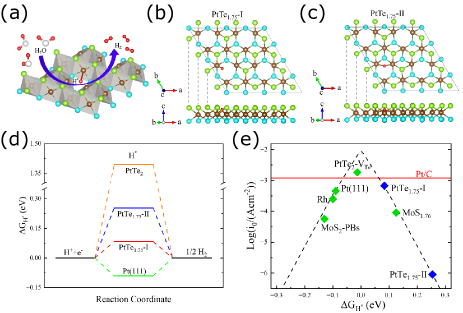
According to the new principle for active catalytic sites Gao et al. (2022); Xu et al. (2021b); Li et al. (2021a), the obstructed bulk states in the patterned monolayer (which can be seen as the limit of obstructed surface states) may bring measured catalytic activity. By exposing undercoordinated atoms as the active sites, vacancy engineering is an important strategy to optimize the HER performance of the basal planes in 2D materials Li et al. (2021b); Jiang et al. (2022). As the acidic HER of the PtTe1.75 schematized in Fig. 4(a), protons (H+) in solution generate adsorbed H atoms (H∗) as intermediate, then the H atoms on the catalyst surface are desorbed to produce hydrogen (H2), which can be formulized as
| (2) |
Here ‘‘*’’ denotes some site on the surface, i.e., a ‘‘*" by itself denotes a free site, while H∗ denotes a hydrogen atom absorbed on the surface. Te vacancy induced states near give PtTe1.75 monolayer larger electrical conductivity than pristine PtTe2 monolayer, which will effectively facilitate electron transfer for HER. We used a 22 PtTe1.75 supercell to simulate the basal plane. Compared with the fully coordinated Te atoms, H atoms are more likely to be adsorbed near the undercoordinated Pt atoms, just as the most stable and metastable structures shown in Fig. 4(b) and Fig. 4(c). As an important descriptor of HER activity Nørskov et al. (2005); Greeley et al. (2006), the change of Gibbs free energy induced by hydrogen adsorption () can be defined as Nørskov et al. (2004)
| (3) | ||||
where E is internal Energy, ZPE is zero-point energy, is the correction of enthalpy, T is temperature, while S denotes entropy. An ideal catalyst for HER should host a near-zero , which can effectively maintain the balance between adsorption and desorption steps Greeley et al. (2006). As shown in Fig. 4(d), unlike pristine PtTe2 monolayer with a large positive due to its extremely inert basal plane, the PtTe1.75 monolayer hosts an optimal (0.08 eV), which is slightly superior to the benchmark material Pt ( = -0.09 eV) Nørskov et al. (2005). Thus, the active Pt sites induced by Te vacancy greatly optimize hydrogen adsorption in the intermediate, which will significantly improve HER performance Lei et al. (2021). According to Nørskov et al. Nørskov et al. (2005), the theoretical exchange current density () as a function of is calculated. As shown in Fig. 4(e), the PtTe1.75 monolayer approaches the volcanic peak from the right with , which is comparable to commercial Pt/C catalyst () Yang et al. (2021). Therefore, Te vacancy can greatly stimulate the catalytic activity of PtTe2 basal plane and produce excellent HER performance.
IV Discussion
The PtTe2 system and its derivatives (the monolayer, multilayer and doped systems) have gained lots of attention since various fascinating properties in them have been proposed, such as type-II Dirac fermion, ultrahigh electrical conductivity, tunability and superconductivity, and so on. In this work, we find that the PtTe1.75 hosts not only unique band structures with three lower-energy bands belonging to BRs (induced by the vacancy), but also large SHC effect and excellent HER performance. First, we have calculated the corresponding time reversal invariant which indicates the 2D TI nature in the patterned PtTe2 monolayer. We demonstrate that the topological phase can be deduced by a gap closing and reopening process with the evolution of the strength of SOC from (without SOC) to (with SOC). The critical phase transition occurs at , which gives a sextuplet of critical WPs. Second, the Te vacancy breaks and induces Rashba SOC band splitting. The estimated momentum offset is super large with Å-1. Third, we find that the SHC is as large as 1.25 at . Furthermore, the SHC varies quickly and almost monotonically from -1.2 to 3.1 , indicating that the SHC in the patterned PtTe2 monolayer can be conveniently tuned for various applications. Lastly, we also find the Te vacancy in the patterned monolayer can induce excellent HER activity. These results not only offer a new idea to search 2D materials with large SHC, i.e., by introducing inversion-symmetry breaking vacancies in large SOC systems, but also provide a feasible system for the potential application in spintronics and HER catalysts.
Acknowledgments
This work was supported by the National Natural Science Foundation of China (Grants No. 11974395, No. 12188101, No. 52188101 and No. 51725103), the Strategic Priority Research Program of Chinese Academy of Sciences (Grant No. XDB33000000), and the Center for Materials Genome.
Conflict of Interest
The authors declare no conflict of interest.
Data Availability Statement
The datasets used in this article are available from the corresponding author upon request.
References
- Armitage et al. (2018) N. P. Armitage, E. J. Mele, and A. Vishwanath, Rev. Mod. Phys. 90, 015001 (2018).
- Wan et al. (2011) X. Wan, A. M. Turner, A. Vishwanath, and S. Y. Savrasov, Phys. Rev. B 83, 205101 (2011).
- Wang et al. (2013) Z. Wang, H. Weng, Q. Wu, X. Dai, and Z. Fang, Phys. Rev. B 88, 125427 (2013).
- Bradlyn et al. (2016) B. Bradlyn, J. Cano, Z. Wang, M. G. Vergniory, C. Felser, R. J. Cava, and B. A. Bernevig, Science 353, aaf5037 (2016).
- Wieder et al. (2016) B. J. Wieder, Y. Kim, A. M. Rappe, and C. L. Kane, Phys. Rev. Lett. 116, 186402 (2016).
- Yan et al. (2017) M. Yan, H. Huang, K. Zhang, E. Wang, W. Yao, K. Deng, G. Wan, H. Zhang, M. Arita, H. Yang, Z. Sun, H. Yao, Y. Wu, S. Fan, W. Duan, and S. Zhou, Nat. Commun. 8, 257 (2017).
- Politano et al. (2018) A. Politano, G. Chiarello, B. Ghosh, K. Sadhukhan, C.-N. Kuo, C. S. Lue, V. Pellegrini, and A. Agarwal, Phys. Rev. Lett. 121, 086804 (2018).
- Fu et al. (2018) L. Fu, D. Hu, R. G. Mendes, M. H. Rummeli, Q. Dai, B. Wu, and Y. Liu, ACS Nano 12, 9405 (2018).
- (9) S. Hao, J. Zeng, T. Xu, X. Cong, C. Wang, C. Wu, Y. Wang, X. Liu, T. Cao, G. Su, L. Jia, Z. Wu, Q. Lin, L. Zhang, S. Yan, M. Guo, Z. Wang, P. Tan, L. Sun, Z. Ni, S.-J. Liang, X. Cui, and F. Miao, Adv. Funct. Mater. 28, 1803746.
- Lin et al. (2020) M.-K. Lin, R. A. B. Villaos, J. A. Hlevyack, P. Chen, R.-Y. Liu, C.-H. Hsu, J. Avila, S.-K. Mo, F.-C. Chuang, and T.-C. Chiang, Phys. Rev. Lett. 124, 036402 (2020).
- Deng et al. (2019) K. Deng, M. Yan, C.-P. Yu, J. Li, X. Zhou, K. Zhang, Y. Zhao, K. Miyamoto, T. Okuda, W. Duan, Y. Wu, X. Zhong, and S. Zhou, Sci. Bull. 64, 1044 (2019), two-Dimensional Materials: New Opportunities for Electronics, Photonics and Optoelectronics.
- (12) F. Fei, X. Bo, P. Wang, J. Ying, J. Li, K. Chen, Q. Dai, B. Chen, Z. Sun, M. Zhang, F. Qu, Y. Zhang, Q. Wang, X. Wang, L. Cao, H. Bu, F. Song, X. Wan, and B. Wang, Adv. Mater. 30, 1801556.
- Jiang et al. (2020) J. Jiang, S. Lee, F. Fei, F. Song, E. Vescovo, K. Kaznatcheev, F. J. Walker, and C. H. Ahn, APL Mater. 8, 061106 (2020).
- Nie et al. (2018) S. Nie, L. Xing, R. Jin, W. Xie, Z. Wang, and F. B. Prinz, Phys. Rev. B 98, 125143 (2018).
- Tong et al. (2020) X.-W. Tong, Y.-N. Lin, R. Huang, Z.-X. Zhang, C. Fu, D. Wu, L.-B. Luo, Z.-J. Li, F.-X. Liang, and W. Zhang, ACS Appl. Mater. Interfaces 12, 53921 (2020).
- Shawkat et al. (2021) M. S. Shawkat, S. B. Hafiz, M. M. Islam, S. A. Mofid, M. M. Al Mahfuz, A. Biswas, H.-S. Chung, E. Okogbue, T.-J. Ko, D. Chanda, T. Roy, D.-K. Ko, and Y. Jung, ACS Appl. Mater. Interfaces 13, 15542 (2021).
- (17) H. Xu, C. Guo, J. Zhang, W. Guo, C.-N. Kuo, C. S. Lue, W. Hu, L. Wang, G. Chen, A. Politano, X. Chen, and W. Lu, Small 15, 1903362.
- Liu et al. (2021) L. Liu, D. Zemlyanov, and Y. P. Chen, 2D Mater. 8, 045033 (2021).
- Ast et al. (2007) C. R. Ast, J. Henk, A. Ernst, L. Moreschini, M. C. Falub, D. Pacilé, P. Bruno, K. Kern, and M. Grioni, Phys. Rev. Lett. 98, 186807 (2007).
- Blöchl (1994) P. E. Blöchl, Phys. Rev. B 50, 17953 (1994).
- Kresse and Joubert (1999) G. Kresse and D. Joubert, Phys. Rev. B 59, 1758 (1999).
- Kresse and Furthmüller (1996a) G. Kresse and J. Furthmüller, Comput. Mater. Sci. 6, 15 (1996a).
- Kresse and Furthmüller (1996b) G. Kresse and J. Furthmüller, Phys. Rev. B 54, 11169 (1996b).
- Perdew et al. (1996) J. P. Perdew, K. Burke, and M. Ernzerhof, Phys. Rev. Lett. 77, 3865 (1996).
- Yu et al. (2011) R. Yu, X. L. Qi, A. Bernevig, Z. Fang, and X. Dai, Phys. Rev. B 84, 075119 (2011).
- Koepernik and Eschrig (1999) K. Koepernik and H. Eschrig, Phys. Rev. B 59, 1743 (1999).
- Gao et al. (2021a) J. Gao, Q. Wu, C. Persson, and Z. Wang, Comput. Phys. Commun. 261, 107760 (2021a).
- Nie et al. (2021a) S. Nie, Y. Qian, J. Gao, Z. Fang, H. Weng, and Z. Wang, Phys. Rev. B 103, 205133 (2021a).
- Nie et al. (2021b) S. Nie, B. A. Bernevig, and Z. Wang, Phys. Rev. Research 3, L012028 (2021b).
- Gao et al. (2022) J. Gao, Y. Qian, H. Jia, Z. Guo, Z. Fang, M. Liu, H. Weng, and Z. Wang, Sci. Bull. 67, 598 (2022).
- Xu et al. (2021a) Y. Xu, L. Elcoro, Z.-D. Song, M. G. Vergniory, C. Felser, S. S. P. Parkin, N. Regnault, J. L. Manes, and B. A. Bernevig, arXiv:2106.10276v1 (2021a).
- Kane and Mele (2005a) C. L. Kane and E. J. Mele, Phys. Rev. Lett. 95, 146802 (2005a).
- Kane and Mele (2005b) C. L. Kane and E. J. Mele, Phys. Rev. Lett. 95, 226801 (2005b).
- Guo et al. (2021) Z. Guo, D. Yan, H. Sheng, S. Nie, Y. Shi, and Z. Wang, Phys. Rev. B 103, 115145 (2021).
- Wang et al. (2021) X. Wang, D. Geng, D. Yan, W. Hu, H. Zhang, S. Yue, Z. Sun, S. Kumar, E. F. Schwier, K. Shimada, P. Cheng, L. Chen, S. Nie, Z. Wang, Y. Shi, Y.-Q. Zhang, K. Wu, and B. Feng, Phys. Rev. B 104, L241408 (2021).
- Zhang et al. (2009) H. Zhang, C.-X. Liu, X.-L. Qi, X. Dai, Z. Fang, and S.-C. Zhang, Nat. Phys. 5, 438 (2009).
- Shao et al. (2021) D. Shao, Z. Guo, X. Wu, S. Nie, J. Sun, H. Weng, and Z. Wang, Phys. Rev. Research 3, 013278 (2021).
- Bradlyn et al. (2017) B. Bradlyn, L. Elcoro, J. Cano, M. G. Vergniory, Z. Wang, C. Felser, M. I. Aroyo, and B. A. Bernevig, Nature 547, 298 (2017).
- Deng et al. (2022) J. Deng, D. Shao, J. Gao, C. Yue, H. Weng, Z. Fang, and Z. Wang, Phys. Rev. B 105, 224103 (2022).
- Qian et al. (2020) Y. Qian, J. Gao, Z. Song, S. Nie, Z. Wang, H. Weng, and Z. Fang, Phys. Rev. B 101, 155143 (2020).
- Gao et al. (2021b) J. Gao, Y. Qian, S. Nie, Z. Fang, H. Weng, and Z. Wang, Sci. Bull. 66, 667 (2021b).
- Nie et al. (2020) S. Nie, Y. Sun, F. B. Prinz, Z. Wang, H. Weng, Z. Fang, and X. Dai, Phys. Rev. Lett. 124, 076403 (2020).
- Shi et al. (2021) W. Shi, B. J. Wieder, H. L. Meyerheim, Y. Sun, Y. Zhang, Y. Li, L. Shen, Y. Qi, L. Yang, J. Jena, P. Werner, K. Koepernik, S. Parkin, Y. Chen, C. Felser, B. A. Bernevig, and Z. Wang, Nat. Phys. 17, 381 (2021).
- Zhang et al. (2017) Y. Zhang, Y. Sun, H. Yang, J. Železný, S. P. P. Parkin, C. Felser, and B. Yan, Phys. Rev. B 95, 075128 (2017).
- Xiao et al. (2010) D. Xiao, M.-C. Chang, and Q. Niu, Rev. Mod. Phys. 82, 1959 (2010).
- King-Smith and Vanderbilt (1993) R. D. King-Smith and D. Vanderbilt, Phys. Rev. B 47, 1651 (1993).
- Vanderbilt and King-Smith (1993) D. Vanderbilt and R. D. King-Smith, Phys. Rev. B 48, 4442 (1993).
- Vanderbilt (2018) D. Vanderbilt, Berry Phases in Electronic Structure Theory: Electric Polarization, Orbital Magnetization and Topological Insulators (Cambridge University Press, Cambridge, 2018).
- Xu et al. (2021b) Y. Xu, L. Elcoro, G. Li, Z.-D. Song, N. Regnault, Q. Yang, Y. Sun, S. Parkin, C. Felser, and B. A. Bernevig, arXiv:2111.02433v1 (2021b).
- Li et al. (2021a) G. Li, Y. Xu, Z. Song, Q. Yang, U. Gupta, V. S, Y. Sun, P. Sessi, S. S. P. Parkin, B. A. Bernevig, and C. Felser, arXiv:2111.02435v1 (2021a).
- Li et al. (2021b) X. Li, Y. Fang, J. Wang, H. Fang, S. Xi, X. Zhao, D. Xu, H. Xu, W. Yu, X. Hai, C. Chen, C. Yao, H. B. Tao, A. G. R. Howe, S. J. Pennycook, B. Liu, J. Lu, and C. Su, Nat. Commun. 12, 2351 (2021b).
- Jiang et al. (2022) L. Jiang, Q. Zhou, J.-J. Li, Y.-X. Xia, H.-X. Li, and Y.-J. Li, ACS Appl. Nano Mater. 5, 3521 (2022).
- Nørskov et al. (2005) J. K. Nørskov, T. Bligaard, A. Logadottir, J. R. Kitchin, J. G. Chen, S. Pandelov, and U. Stimming, J. Electrochem. Soc. 152, J23 (2005).
- Greeley et al. (2006) J. Greeley, T. F. Jaramillo, J. Bonde, I. Chorkendorff, and J. K. Nørskov, Nat. Mater. 5, 909 (2006).
- Nørskov et al. (2004) J. K. Nørskov, J. Rossmeisl, A. Logadottir, L. Lindqvist, J. R. Kitchin, T. Bligaard, and H. Jonsson, J. Phys. Chem. B 108, 17886 (2004).
- Lei et al. (2021) B. Lei, Y. Y. Zhang, and S. X. Du, Chin. Phys. B 29, 058104 (2021).
- Yang et al. (2021) Q. Yang, G. Li, Y. Zhang, J. Liu, J. Rao, T. Heine, C. Felser, and Y. Sun, npj Comput. Mater. 7, 207 (2021).
- Zhu et al. (2019) J. Zhu, Z.-C. Wang, H. Dai, Q. Wang, R. Yang, H. Yu, M. Liao, J. Zhang, W. Chen, Z. Wei, N. Li, L. Du, D. Shi, W. Wang, L. Zhang, Y. Jiang, and G. Zhang, Nat. Commun. 10, 1348 (2019).
- Sancho et al. (1985) M. P. L. Sancho, J. M. L. Sancho, J. M. L. Sancho, and J. Rubio, J. Phys. F: Met. Phys. 15, 851 (1985).
- Marzari et al. (2012) N. Marzari, A. A. Mostofi, J. R. Yates, I. Souza, and D. Vanderbilt, Rev. Mod. Phys. 84, 1419 (2012).
- Wu et al. (2018) Q. Wu, S. Zhang, H.-F. Song, M. Troyer, and A. A. Soluyanov, Comput. Phys. Commun. 224, 405 (2018).
SUPPLEMENTARY MATERIAL
A Lattice parameters of the patterned PtTe2 monolayer with a Te vacancy
The pristine PtTe2 system crystallizes in the CdI2-type trigonal (1T) structure (SG Pm1) is a layered material stacking along the axis. Recently, the monolayer structure with kagome lattice formed by one Te vacancy in the 22 supercell has been successfully grown Liu et al. (2021). The patterned PtTe2 monolayer contains two Te layers, with 4 Te atoms in the bottom layer while 3 Te atoms in the top layer, as shown in Fig. 2(a). The corresponding lattice parameters are , , and the thickness of the vacuum layer along axis was set to Å, with denoting the distance between the bottom Te layer and the top Te layer.
| Atoms | Wyckoff positions | Fractional coordinates |
|---|---|---|
| Pt1 | 1c | (0.66667,0.33333,0.0) |
| Pt2 | 3d | (0.16667,0.33333,0.0) |
| Te1(bottom) | 1a | (0.00000,0.00000,-0.04542) |
| Te2(bottom) | 3d | (0.50000,0.50000,-0.04542) |
| Te3(top) | 3d | (0.83333,0.66667,0.04542) |
B The calculated weak topological invariant
To characterize the topological properties in the patterned PtTe2 monolayer, the weak topological invariants are calculated by the 1D Wilson loop method. Taking Te: 5s25p4 and Pt: 5d96s1 orbitals into consideration, there are valance electrons, resulting in valence bands. From Figs. S1(a-d), the calculated weak topological invariants for 78, 80, 82 and 84 (corresponds to , , and ) occupied bands are , , and , respectively. Thus, the patterned PtTe2 monolayer with valence bands is a 2D TI with .

C Topological surface states of the patterned PtTe2 monolayer
Exotic topological surface states serve as significant fingerprints to identify various topological phases. Based on the tight-binding (TB) model constructed with the maximally localised Wannier functions and surface Green function methods Sancho et al. (1985); Marzari et al. (2012); Wu et al. (2018), we have calculated the corresponding surface states to identify the nature of 2D TI.
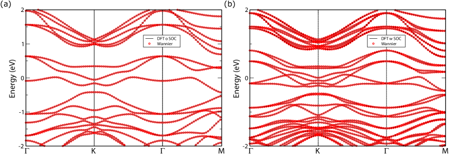
As shown in Fig.S2(a,b), we have chosen Pt-d and Te-p orbitals as the projected bases of the wannier-based TB model, which can reproduce the DFT band structures perfectly. As expected, the helical edge states corresponds to the 2D TI can be found in the (01) edge states, as shown in Fig. S3(b) and Fig. S3(d).
D Band structures vs. dopping
Since the electronic properties and SHC of the patterned PtTe2 monolayer are sensitive to the , we can adopt different dopings at the Te-vacancy position to tune EF effectively.
As shown in Figs. S4(a-c), we can find that both the introduced Pb doping and Tl doping behave as electron dopings, which increase the significantly. The decreased magnitude of the EF are estimated to be 0.482232 eV and 0.256149 eV, respectively.
